EP0500351A2 - Halbleiterlaser - Google Patents
Halbleiterlaser Download PDFInfo
- Publication number
- EP0500351A2 EP0500351A2 EP92301373A EP92301373A EP0500351A2 EP 0500351 A2 EP0500351 A2 EP 0500351A2 EP 92301373 A EP92301373 A EP 92301373A EP 92301373 A EP92301373 A EP 92301373A EP 0500351 A2 EP0500351 A2 EP 0500351A2
- Authority
- EP
- European Patent Office
- Prior art keywords
- active layer
- layer
- cladding layer
- semiconductor
- cladding
- Prior art date
- Legal status (The legal status is an assumption and is not a legal conclusion. Google has not performed a legal analysis and makes no representation as to the accuracy of the status listed.)
- Granted
Links
Images


Classifications
-
- H—ELECTRICITY
- H10—SEMICONDUCTOR DEVICES; ELECTRIC SOLID-STATE DEVICES NOT OTHERWISE PROVIDED FOR
- H10H—INORGANIC LIGHT-EMITTING SEMICONDUCTOR DEVICES HAVING POTENTIAL BARRIERS
- H10H20/00—Individual inorganic light-emitting semiconductor devices having potential barriers, e.g. light-emitting diodes [LED]
- H10H20/80—Constructional details
- H10H20/81—Bodies
- H10H20/822—Materials of the light-emitting regions
- H10H20/824—Materials of the light-emitting regions comprising only Group III-V materials, e.g. GaP
-
- H—ELECTRICITY
- H01—ELECTRIC ELEMENTS
- H01S—DEVICES USING THE PROCESS OF LIGHT AMPLIFICATION BY STIMULATED EMISSION OF RADIATION [LASER] TO AMPLIFY OR GENERATE LIGHT; DEVICES USING STIMULATED EMISSION OF ELECTROMAGNETIC RADIATION IN WAVE RANGES OTHER THAN OPTICAL
- H01S5/00—Semiconductor lasers
- H01S5/20—Structure or shape of the semiconductor body to guide the optical wave ; Confining structures perpendicular to the optical axis, e.g. index or gain guiding, stripe geometry, broad area lasers, gain tailoring, transverse or lateral reflectors, special cladding structures, MQW barrier reflection layers
- H01S5/22—Structure or shape of the semiconductor body to guide the optical wave ; Confining structures perpendicular to the optical axis, e.g. index or gain guiding, stripe geometry, broad area lasers, gain tailoring, transverse or lateral reflectors, special cladding structures, MQW barrier reflection layers having a ridge or stripe structure
- H01S5/223—Buried stripe structure
- H01S5/2231—Buried stripe structure with inner confining structure only between the active layer and the upper electrode
-
- H—ELECTRICITY
- H01—ELECTRIC ELEMENTS
- H01S—DEVICES USING THE PROCESS OF LIGHT AMPLIFICATION BY STIMULATED EMISSION OF RADIATION [LASER] TO AMPLIFY OR GENERATE LIGHT; DEVICES USING STIMULATED EMISSION OF ELECTROMAGNETIC RADIATION IN WAVE RANGES OTHER THAN OPTICAL
- H01S5/00—Semiconductor lasers
- H01S5/30—Structure or shape of the active region; Materials used for the active region
- H01S5/32—Structure or shape of the active region; Materials used for the active region comprising PN junctions, e.g. hetero- or double- heterostructures
- H01S5/323—Structure or shape of the active region; Materials used for the active region comprising PN junctions, e.g. hetero- or double- heterostructures in AIIIBV compounds, e.g. AlGaAs-laser, InP-based laser
- H01S5/32308—Structure or shape of the active region; Materials used for the active region comprising PN junctions, e.g. hetero- or double- heterostructures in AIIIBV compounds, e.g. AlGaAs-laser, InP-based laser emitting light at a wavelength less than 900 nm
- H01S5/32325—Structure or shape of the active region; Materials used for the active region comprising PN junctions, e.g. hetero- or double- heterostructures in AIIIBV compounds, e.g. AlGaAs-laser, InP-based laser emitting light at a wavelength less than 900 nm red laser based on InGaP
-
- H—ELECTRICITY
- H10—SEMICONDUCTOR DEVICES; ELECTRIC SOLID-STATE DEVICES NOT OTHERWISE PROVIDED FOR
- H10H—INORGANIC LIGHT-EMITTING SEMICONDUCTOR DEVICES HAVING POTENTIAL BARRIERS
- H10H20/00—Individual inorganic light-emitting semiconductor devices having potential barriers, e.g. light-emitting diodes [LED]
- H10H20/01—Manufacture or treatment
- H10H20/011—Manufacture or treatment of bodies, e.g. forming semiconductor layers
- H10H20/013—Manufacture or treatment of bodies, e.g. forming semiconductor layers having light-emitting regions comprising only Group III-V materials
-
- H—ELECTRICITY
- H01—ELECTRIC ELEMENTS
- H01S—DEVICES USING THE PROCESS OF LIGHT AMPLIFICATION BY STIMULATED EMISSION OF RADIATION [LASER] TO AMPLIFY OR GENERATE LIGHT; DEVICES USING STIMULATED EMISSION OF ELECTROMAGNETIC RADIATION IN WAVE RANGES OTHER THAN OPTICAL
- H01S5/00—Semiconductor lasers
- H01S5/20—Structure or shape of the semiconductor body to guide the optical wave ; Confining structures perpendicular to the optical axis, e.g. index or gain guiding, stripe geometry, broad area lasers, gain tailoring, transverse or lateral reflectors, special cladding structures, MQW barrier reflection layers
- H01S5/22—Structure or shape of the semiconductor body to guide the optical wave ; Confining structures perpendicular to the optical axis, e.g. index or gain guiding, stripe geometry, broad area lasers, gain tailoring, transverse or lateral reflectors, special cladding structures, MQW barrier reflection layers having a ridge or stripe structure
- H01S5/2201—Structure or shape of the semiconductor body to guide the optical wave ; Confining structures perpendicular to the optical axis, e.g. index or gain guiding, stripe geometry, broad area lasers, gain tailoring, transverse or lateral reflectors, special cladding structures, MQW barrier reflection layers having a ridge or stripe structure in a specific crystallographic orientation
-
- H—ELECTRICITY
- H01—ELECTRIC ELEMENTS
- H01S—DEVICES USING THE PROCESS OF LIGHT AMPLIFICATION BY STIMULATED EMISSION OF RADIATION [LASER] TO AMPLIFY OR GENERATE LIGHT; DEVICES USING STIMULATED EMISSION OF ELECTROMAGNETIC RADIATION IN WAVE RANGES OTHER THAN OPTICAL
- H01S5/00—Semiconductor lasers
- H01S5/20—Structure or shape of the semiconductor body to guide the optical wave ; Confining structures perpendicular to the optical axis, e.g. index or gain guiding, stripe geometry, broad area lasers, gain tailoring, transverse or lateral reflectors, special cladding structures, MQW barrier reflection layers
- H01S5/22—Structure or shape of the semiconductor body to guide the optical wave ; Confining structures perpendicular to the optical axis, e.g. index or gain guiding, stripe geometry, broad area lasers, gain tailoring, transverse or lateral reflectors, special cladding structures, MQW barrier reflection layers having a ridge or stripe structure
- H01S5/2205—Structure or shape of the semiconductor body to guide the optical wave ; Confining structures perpendicular to the optical axis, e.g. index or gain guiding, stripe geometry, broad area lasers, gain tailoring, transverse or lateral reflectors, special cladding structures, MQW barrier reflection layers having a ridge or stripe structure comprising special burying or current confinement layers
- H01S5/2206—Structure or shape of the semiconductor body to guide the optical wave ; Confining structures perpendicular to the optical axis, e.g. index or gain guiding, stripe geometry, broad area lasers, gain tailoring, transverse or lateral reflectors, special cladding structures, MQW barrier reflection layers having a ridge or stripe structure comprising special burying or current confinement layers based on III-V materials
- H01S5/2209—GaInP based
-
- H—ELECTRICITY
- H01—ELECTRIC ELEMENTS
- H01S—DEVICES USING THE PROCESS OF LIGHT AMPLIFICATION BY STIMULATED EMISSION OF RADIATION [LASER] TO AMPLIFY OR GENERATE LIGHT; DEVICES USING STIMULATED EMISSION OF ELECTROMAGNETIC RADIATION IN WAVE RANGES OTHER THAN OPTICAL
- H01S5/00—Semiconductor lasers
- H01S5/20—Structure or shape of the semiconductor body to guide the optical wave ; Confining structures perpendicular to the optical axis, e.g. index or gain guiding, stripe geometry, broad area lasers, gain tailoring, transverse or lateral reflectors, special cladding structures, MQW barrier reflection layers
- H01S5/22—Structure or shape of the semiconductor body to guide the optical wave ; Confining structures perpendicular to the optical axis, e.g. index or gain guiding, stripe geometry, broad area lasers, gain tailoring, transverse or lateral reflectors, special cladding structures, MQW barrier reflection layers having a ridge or stripe structure
- H01S5/2205—Structure or shape of the semiconductor body to guide the optical wave ; Confining structures perpendicular to the optical axis, e.g. index or gain guiding, stripe geometry, broad area lasers, gain tailoring, transverse or lateral reflectors, special cladding structures, MQW barrier reflection layers having a ridge or stripe structure comprising special burying or current confinement layers
- H01S5/2206—Structure or shape of the semiconductor body to guide the optical wave ; Confining structures perpendicular to the optical axis, e.g. index or gain guiding, stripe geometry, broad area lasers, gain tailoring, transverse or lateral reflectors, special cladding structures, MQW barrier reflection layers having a ridge or stripe structure comprising special burying or current confinement layers based on III-V materials
- H01S5/221—Structure or shape of the semiconductor body to guide the optical wave ; Confining structures perpendicular to the optical axis, e.g. index or gain guiding, stripe geometry, broad area lasers, gain tailoring, transverse or lateral reflectors, special cladding structures, MQW barrier reflection layers having a ridge or stripe structure comprising special burying or current confinement layers based on III-V materials containing aluminium
-
- H—ELECTRICITY
- H01—ELECTRIC ELEMENTS
- H01S—DEVICES USING THE PROCESS OF LIGHT AMPLIFICATION BY STIMULATED EMISSION OF RADIATION [LASER] TO AMPLIFY OR GENERATE LIGHT; DEVICES USING STIMULATED EMISSION OF ELECTROMAGNETIC RADIATION IN WAVE RANGES OTHER THAN OPTICAL
- H01S5/00—Semiconductor lasers
- H01S5/20—Structure or shape of the semiconductor body to guide the optical wave ; Confining structures perpendicular to the optical axis, e.g. index or gain guiding, stripe geometry, broad area lasers, gain tailoring, transverse or lateral reflectors, special cladding structures, MQW barrier reflection layers
- H01S5/22—Structure or shape of the semiconductor body to guide the optical wave ; Confining structures perpendicular to the optical axis, e.g. index or gain guiding, stripe geometry, broad area lasers, gain tailoring, transverse or lateral reflectors, special cladding structures, MQW barrier reflection layers having a ridge or stripe structure
- H01S5/2205—Structure or shape of the semiconductor body to guide the optical wave ; Confining structures perpendicular to the optical axis, e.g. index or gain guiding, stripe geometry, broad area lasers, gain tailoring, transverse or lateral reflectors, special cladding structures, MQW barrier reflection layers having a ridge or stripe structure comprising special burying or current confinement layers
- H01S5/2218—Structure or shape of the semiconductor body to guide the optical wave ; Confining structures perpendicular to the optical axis, e.g. index or gain guiding, stripe geometry, broad area lasers, gain tailoring, transverse or lateral reflectors, special cladding structures, MQW barrier reflection layers having a ridge or stripe structure comprising special burying or current confinement layers having special optical properties
- H01S5/2219—Structure or shape of the semiconductor body to guide the optical wave ; Confining structures perpendicular to the optical axis, e.g. index or gain guiding, stripe geometry, broad area lasers, gain tailoring, transverse or lateral reflectors, special cladding structures, MQW barrier reflection layers having a ridge or stripe structure comprising special burying or current confinement layers having special optical properties absorbing
-
- H—ELECTRICITY
- H01—ELECTRIC ELEMENTS
- H01S—DEVICES USING THE PROCESS OF LIGHT AMPLIFICATION BY STIMULATED EMISSION OF RADIATION [LASER] TO AMPLIFY OR GENERATE LIGHT; DEVICES USING STIMULATED EMISSION OF ELECTROMAGNETIC RADIATION IN WAVE RANGES OTHER THAN OPTICAL
- H01S5/00—Semiconductor lasers
- H01S5/20—Structure or shape of the semiconductor body to guide the optical wave ; Confining structures perpendicular to the optical axis, e.g. index or gain guiding, stripe geometry, broad area lasers, gain tailoring, transverse or lateral reflectors, special cladding structures, MQW barrier reflection layers
- H01S5/22—Structure or shape of the semiconductor body to guide the optical wave ; Confining structures perpendicular to the optical axis, e.g. index or gain guiding, stripe geometry, broad area lasers, gain tailoring, transverse or lateral reflectors, special cladding structures, MQW barrier reflection layers having a ridge or stripe structure
- H01S5/223—Buried stripe structure
-
- H—ELECTRICITY
- H01—ELECTRIC ELEMENTS
- H01S—DEVICES USING THE PROCESS OF LIGHT AMPLIFICATION BY STIMULATED EMISSION OF RADIATION [LASER] TO AMPLIFY OR GENERATE LIGHT; DEVICES USING STIMULATED EMISSION OF ELECTROMAGNETIC RADIATION IN WAVE RANGES OTHER THAN OPTICAL
- H01S5/00—Semiconductor lasers
- H01S5/30—Structure or shape of the active region; Materials used for the active region
- H01S5/32—Structure or shape of the active region; Materials used for the active region comprising PN junctions, e.g. hetero- or double- heterostructures
- H01S5/3202—Structure or shape of the active region; Materials used for the active region comprising PN junctions, e.g. hetero- or double- heterostructures grown on specifically orientated substrates, or using orientation dependent growth
-
- H—ELECTRICITY
- H01—ELECTRIC ELEMENTS
- H01S—DEVICES USING THE PROCESS OF LIGHT AMPLIFICATION BY STIMULATED EMISSION OF RADIATION [LASER] TO AMPLIFY OR GENERATE LIGHT; DEVICES USING STIMULATED EMISSION OF ELECTROMAGNETIC RADIATION IN WAVE RANGES OTHER THAN OPTICAL
- H01S5/00—Semiconductor lasers
- H01S5/30—Structure or shape of the active region; Materials used for the active region
- H01S5/32—Structure or shape of the active region; Materials used for the active region comprising PN junctions, e.g. hetero- or double- heterostructures
- H01S5/3206—Structure or shape of the active region; Materials used for the active region comprising PN junctions, e.g. hetero- or double- heterostructures ordering or disordering the natural superlattice in ternary or quaternary materials
- H01S5/3207—Structure or shape of the active region; Materials used for the active region comprising PN junctions, e.g. hetero- or double- heterostructures ordering or disordering the natural superlattice in ternary or quaternary materials ordered active layer
-
- H—ELECTRICITY
- H01—ELECTRIC ELEMENTS
- H01S—DEVICES USING THE PROCESS OF LIGHT AMPLIFICATION BY STIMULATED EMISSION OF RADIATION [LASER] TO AMPLIFY OR GENERATE LIGHT; DEVICES USING STIMULATED EMISSION OF ELECTROMAGNETIC RADIATION IN WAVE RANGES OTHER THAN OPTICAL
- H01S5/00—Semiconductor lasers
- H01S5/30—Structure or shape of the active region; Materials used for the active region
- H01S5/32—Structure or shape of the active region; Materials used for the active region comprising PN junctions, e.g. hetero- or double- heterostructures
- H01S5/3211—Structure or shape of the active region; Materials used for the active region comprising PN junctions, e.g. hetero- or double- heterostructures characterised by special cladding layers, e.g. details on band-discontinuities
Definitions
- the present invention relates to a semiconductor laser using Group V-III compound semiconductor materials and, more particularly, to a semiconductor laser using InGaAfP materials in a double hetero structure.
- a decrease in oscillation threshold value of a semiconductor laser and an improvement of temperature characteristics are very important in consideration of an increase in service life.
- the threshold value of laser oscillation and the temperature characteristics depend on enclosure of carriers in an active layer, especially, leakage of electrons having a small effective mass to a p-type cladding layer is necessarily suppressed.
- band discontinuity between the conduction band of an active layer and that of a p-type cladding layer can be sufficiently increased. Since this discontinuity effectively prevents leakage of electrons from the active layer to the p-type cladding layer, an increase in oscillation threshold value is not a serious problem in the GaAfAs semiconductor laser.
- the InGaAf P materials have characteristics in which discontinuity of the conduction bands is smaller than that of the conventional GaAf As materials. Therefore, leakage of electrons to the p-type cladding layer have not been sufficiently prevented by the band discontinuity, and it has been understood that effective enclosure of carriers is not easily obtained in the InGaAlP-based materials.
- band discontinuity between an active layer and a p-type cladding layer cannot be sufficiently increased, carriers cannot be easily enclosed in the active layer, and the temperature characteristics of the laser cannot be easily improved.
- the present invention has been made in consideration of the above circumstances, and has as its object to provide a semiconductor laser capable of increasing band discontinuity between an active layer and a p-type cladding layer to improve temperature characteristics of the laser.
- formation of ordered structures in an active layer and a p-type cladding layer is controlled to increase band discontinuity between the active layer and the p-type cladding layer.
- a semiconductor laser having a double hetero structure obtained by sandwiching an active layer made of an InGaAf P material or the like between p- and n-type cladding layers has the following characteristics. That is, in the double hetero structure, an ordered structure having regularity in the ⁇ 111> orientation is formed in the active layer and no ordered structure is formed in the p-type cladding layer.
- an arrangement of Group III atoms have regularity by changing growth conditions such as a growth temperature and a ratio of molar flow rate of group-V to group-III sources (V/III) ratio) (for example, J. Crystal Growth 93 (1988) P. 406).
- This regularity is generally called an ordered structure or a natural superlattice.
- the InGaAf P materials have a zinc blend structure, Group III atoms (In, Ga, Af) are generally arranged at random in group-III sublattices (this is called a disordered structure in contrast to the ordered structure).
- Group III atoms In, Ga, Af
- group-III sublattices this is called a disordered structure in contrast to the ordered structure.
- the period of a lattice in the ⁇ 111 > orientation i.e., a lattice constant, depends on the periods of Group III atoms and Group V atoms and has one value a.
- the ordered structure has a structure in which an In rich surface and a Ga (of Af) rich surface are formed in four directions ( ⁇ 111>, ⁇ 1 1 1>, ⁇ 11 1 >, ⁇ 111 >), independent of a substrate orientation. The relationship between these four directions are shown in Fig. 2.
- the ⁇ 111 > direction is perpendicular to (111) surface.
- This structure is defined as an ordered structure of the ⁇ 111> direction.
- the ordered structure is not formed in all crystal grains but present as a domain. In this case, the period of the lattice constant, depends on the regularity of arrangement of Group III atoms and has two values a and 2a.
- the band-gap energy (Eg) of a material is changed.
- the Eg is smaller than that of an InGaAf P material in which the ordered structure is not formed.
- an ordered structure is formed in an active layer, and no ordered structure is formed in a p-type cladding layer, such that band discontinuity between the active layer and the p-type cladding layer is increased.
- growth conditions under which the active layer and the p-type cladding layer are grown are changed to control the formation of the ordered structure.
- the Eg of the active layer was 1.91 eV when no ordered structure was formed in the active layer.
- the smallest Eg was 1.85 eV.
- an Eg of the layer was 2.33 eV when no ordered structure was formed in an In 0.5 (Ga 0.3 Al 0.7 ) 0.5 P layer used as a p-type cladding layer.
- the smallest Eg of the layer was 2.33 eV when the In 0.5 (Ga 0.3 Al 0.7 ) 0.5 P layer had an ordered structure of the ⁇ 111> direction.
- a difference in band-gap energy Eg between the active layer and the p-type cladding layer, both of which have no ordered structure is 0.42 eV.
- a difference in band-gap energy Eg between the active layer and the p-type cladding layer, both of which have ordered structures of the ⁇ 111> direction is about 0.38 to 0.40 eV.
- band discontinuity in conduction band effectively functions to prevent leakage of electrons from the active layer to the p-type cladding layer, i.e., to enclose carriers.
- the difference in band-gap energy Eg between the active layer and the p-type cladding layer is used as an evaluation standard of the band discontinuity for convenience.
- the band discontinuity between the active layer and the p-type cladding layer can be increased, and carriers can be effectively enclosed in the active layer, a reduction of the threshold value of a laser and an improvement of temperature characteristics can be expected.
- an ordered structure of the ⁇ 111> direction is formed in the active layer, and no ordered structure is formed in the p-type cladding layer, such that band discontinuity between the p-type cladding layer and the active layer can be increased. Therefore, overflow of electrons can be effectively suppressed, and a semiconductor laser having preferable temperature characteristics can be obtained.
- Fig. 1 is a sectional view showing a schematic structure of an InGaAf P semiconductor laser according to the first embodiment of the present invention.
- reference numeral 10 denotes an n-type GaAs substrate.
- an n-type In 0.5 (Ga 0.3 Al 0.7 ) 0.5 P cladding layer 11 carrier concentration: 4 x 10 17 cm- 3 ; thickness: 1.2 pm), an ln o . 5 Ga o .
- the substrate 10 has the (100) plane as shown in Fig. 2, an ordered structure of the ⁇ 111> > direction is formed in the active layer 12, and no ordered structure is formed in the p-type cladding layer 13.
- the substrate 10 does not necessarily have the (100) plane, and the substrate 10 may have a plane which is slightly inclined from the (100) plane by, e.g., 5°.
- the p-type cladding layer 13 is etched halfway to form a stripe-like ridge portion.
- This ridge portion has a bottom width of 5 ⁇ m, and the distance between the bottom of the ridge portion and the active layer 12 is 0.3 ⁇ m.
- N-type GaAs current blocking layers 14 (carrier concentration: 2 x 10 18 cm-3; thickness: 1 ⁇ m) are grown and formed on side surfaces of the ridge portion, and a p-type GaAs contact layer 15 (carrier concentration: 2 x 10 18 cm- 3 ; thickness: 3 ⁇ m) is formed on the upper surfaces of the ridge portion and the current blocking layers 14.
- An n-side electrode 16 is formed on the lower surface of the substrate 10, and a p-side electrode 17 is formed on the contact layer 15.
- the structure shown in Fig. 1 is grown by a low-pressure MOCVD method. According to an experiment performed by the present inventors, the following relationship was found between a band-gap energy and growth conditions under which the active layer 12 and the p-type cladding layer 13 were grown.
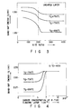
- Fig. 3 shows a relationship between a V/III ratio (a ratio of molar flow rate of PH 3 to group-III sources when the active layer 12 is grown) and a band-gap energy Eg of the active layer 12.
- Growth temperatures (Tg) were set at 690°C, 730°C,and 750°C. Even when any growth temperature (Tg) is set, when the V/III ratio is 200 or more, the band-gap energy Eg is sharply decreased. This is because an ordered structure of the ⁇ 111 > direction is easily formed when the V/III ratio is 200 or more.
- the Eg is increased in accordance with an increase in growth temperature because an ordered structure is not easily formed at a high growth temperature.
- Fig. 4 shows a relationship between a carrier concentration and a band-gap energy Eg of the p-type cladding layer 13.
- the Eg was increased in accordance with an increase in carrier concentration, and the Eg had a constant value, i.e., 2.33 eV, when the carrier concentration was 7 x 10 17 cm- 3 or more.
- a p-type dopant has an effect to prevent the formation of an ordered structure in accordance with an increase in carrier concentration.
- growth conditions under which the laser according to this embodiment shown in Fig. 1 was grown was defined as follows. That is, a growth temperature was set at 690°C, a V/III ratio was set to be 400, and a doping concentration of the p-type cladding layer 13 was set to be 8 x 10 17 cm- 3 . At this time, the band-gap energies of the active layer 12 and the p-type cladding layer 13 were 1.85 eV and 2.33 eV, respectively. Although an ordered structure of the ⁇ 111> direction was formed in the active layer 12, no ordered structure was formed in the p-type cladding layer 13, such that an Eg difference between these layers was 0.48 eV.
- the band-gap energies of the layers were 1.91 eV and 2.33 eV, respectively, and the Eg difference was 0.42.
- a growth temperature was set at 750°C
- a V/III ratio was set to be 100
- the carrier concentration of the p-type cladding layer was set to be 4 x 10 17 cm- 3 .
- a maximum continuous oscillation temperature was as low as 40°C, and life performance was not good.
- band continuity was measured to be 0.38 to 0.40 eV.
- the maximum continuous oscillation temperature of a laser grown under the above growth conditions was as low as 30°C.
- band discontinuity between the active layer 12 and the p-type cladding layer 13 can be increased. For this reason, overflow of electrons can be effectively suppressed, and an InGaAf P semiconductor laser having preferable temperature characteristics can be obtained. Therefore, the industrial effect of the semiconductor laser is extremely large.
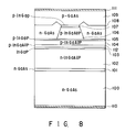
- Fig. 5 is a sectional view showing a schematic structure of a semiconductor laser according to the second embodiment of the present invention.
- reference numeral 100 denotes an n-type GaAs substrate; 101, an n-type GaAs buffer layer; 102, an n-type In 0.5 (Ga 0.3 Al 0.7 ) 0.5 P cladding layer; 103, an ln o . 5 Ga o . 5 P active layer; 104, a p-type In 0,5 (Ga 0.3 Al 0.7 ) 0.5 P first cladding layer; 105, a p-type ln o . 5 Ga o .
- etching stop layer 106, a p-type In 0.5 (Ga 0.3 Al 0.7 ) 0.5 P second cladding layer; 107, a p-type In o . S Ga o . 5 5P cap layer; 108, an n-type GaAs current blocking layer; 109, a p-type GaAs contact layer; 110, an n-type electrode; and 111, a p-type electrode.
- An ordered structure of the ⁇ 111> direction is formed in the active layer 103, and no ordered structure of the ⁇ 111> direction is formed in the first p-type cladding layer 104.
- the structure shown in Fig. 5 is grown by a low-pressure MOCVD method, and formation of the ordered structure of the ⁇ 111> direction is controlled by changing conditions for growing the active layer 103 and the first p-type cladding layer 104.
- Fig. 6 shows a relationship between a growth rate and a band-gap energy (Eg) in growing the active layer.
- Growth temperatures (Tg) were set at 690°C, 730°C, and 750°C, respectively. At any growth temperature, the Eg was sharply decreased when the growth rate becomes 3 wm/h or more, because an ordered structure of the ⁇ 111> direction was easily formed when the growth rate becomes 3 wm/h or more.
- the Eg was increased in accordance with an increase in growth temperature because an ordered structure was not easily formed at a high growth temperature (Tg). In an InGaP layer having an Eg of 1.91 eV, no ordered structure was formed. In an InGaP layerwhich was grown at a growth temperature of 690°C and a growth rate of 3 wm/h or more, an ordered structure was formed most strongly. At this time, an Eg of 1.85 eV was obtained.
- Fig. 7 shows a relationship between a band-gap energy (Eg) and a growth rate in the p-type cladding layer.
- Eg band-gap energy
- the Eg was increased in accordance with a decrease in growth rate, and the Eg had a constant value, i.e., 2.33 eV, at a growth rate of 1 ⁇ m/h or less.
- a sample having an Eg of 2.33 eV no ordered structure was formed. In other samples, an ordered structure was detected.
- a p-type cladding layer 112 having an ordered structure may be formed to have a thickness of 40 nm or less, and the p-type cladding layer 104 having no ordered structure may be formed thereon.
- Zn, Mg, Cd, Be, or the like was used as the p-type dopant, the above effect could be obtained.
- the band-gap energies of the active layer 103 and the first p-type cladding layer 104 which were grown under the above growth conditions were 1.85 eV and 2.33 eV, respectively.
- An ordered structure of the ⁇ 111> direction was formed in the active layer 103, and no ordered structure was formed in the first cladding layer 104, and an Eg difference between these layers was 0.48 eV.
- an oscillation threshold value was 35 mA.
- a high light output of 40 mW was obtained at a temperature up to 80°C.
- conspicuous degradation could not be detected in this semiconductor laser, and it was confirmed that the semiconductor laser was operated for2,000 hours or more.
- the band-gap energies of the layers were 1.91 eV and 2.33 eV, respectively, and an Eg difference of the layers was 0.42 eV.
- a maximum continuous oscillation temperature was as low as 40°C, and the life performance was no good.
- an Eg difference was 0.38 to 0.40 eV.
- a maximum continuous oscillation temperature was as low as 30°C.
- the band-gap energy of the second p-type cladding layer 106 slightly depends on the oscillation threshold value of the laser. For this reason, even when the ordered structure is formed in the second p-type cladding layer 106, no problem occurs. Therefore, the second p-type cladding layer 106 was grown under growth conditions that the growth rate of the layer was increased, thereby suppressing diffusion of a p-type dopant in the active layer 103.
- the buffer layer 101 is made of n-type InGaP
- the etching stop layer 105 is made of n-type InGaAlP, p-type GaAf As, or p-type GaAs
- the cap layer 107 is made of p-type InGaAf P, p-type GaAfAs, or p-type GaAs
- the current blocking layer 108 is made of semi-insulating GaAs or n-type or semi-insulating GaAfAs
- the thickness of the first p-type cladding layer 104 is 0.1 ⁇ m to 0.4 ⁇ m
- the thickness of the active layer 103 is 0.015 ⁇ m to 0.03 ⁇ m.
- this Af composition ratio is properly determined within a range in which the band-gap energy of each of the n- and p-type cladding layers are larger than that of the active layer 103.
- an Af composition ratio X and a composition ratio Y are set to be 0 and 0.5, respectively, the Af composition ratio X and the composition ratio Y may be properly determined within a range in which the band-gap energy of the active layer 103 is smaller than that of the cladding layer.
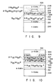
- Figs. 9 to 12 are sectional views showing schematic arrangements of semiconductor lasers according to the third to sixth embodiments of the present invention.
- reference numeral 200 denotes an n-type GaAs substrate; 201, an n-type GaAs buffer layer; 202, an n-type InGaAf P cladding layer; 203, an InGaP active layer in which an ordered structure of the ⁇ 111> direction is formed; 204, a p-type InGaAf P first cladding layer in which no ordered structure is formed; 205, a p-type InGaP etching stop layer; 206, a p-type InGaAf P second cladding layer; 207, a p-type InGaP intermediate band-gap layer; and 208, a p-type contact layer.
- the injected current is squeezed into a ridge portion 209 formed by a p-p hetero barrier between the contact layer 208 and the p-type cladding layer 204.
- a light beam is generated in the active layer 203 substantially along the ridge portion 209 to cause laser oscillation, the beam is enclosed due to an effective refractive index difference between the ridge portion 209 and the outside of the ridge portion 209.
- the same effect as described in the first embodiment can be obtained.
- the buffer layer 201 is made of n-type InGaP
- the active layer 203 is made of n-type InGaAlP
- the etching stop layer 205 is made of p-type GaAfAs
- the intermediate band-gap layer 207 is made of p-type GaAfAs or p-type GaAs
- the same effect as described above can be obtained.
- the composition is expressed as In 1-Y (Ga 1-X Al X ) Y P
- an Af composition ratio X is set to be 0.7.
- this AI composition ratio may be properly determined within a range in which the band-gap energy of each of the cladding layers 202,204, and 206 is sufficiently larger than that of the active layer 203.
- the composition ratios X and Y may be properly determined within a range in which the band-gap energy of the active layer 203 is smaller than that of each of the cladding layers.
- reference numeral 300 denotes an n-type GaAs substrate; 301, an n-type GaAs or n-type InGaP buffer layer; 302, an n-type InGaAfP cladding layer; 303, an InGaP or InGaAfP active layer in which an ordered structure is formed; 304, a p-type InGaAf P first cladding layer in which no ordered structure is formed; 305, a p-type InGaP buffer layer; 306, a p-type InGaAf P second cladding layer; 307, a p-type InGaP or p-type AfGaAs intermediate band-gap layer; 308, an n-type semi-insulating GaAs or n-type GaAfAs current blocking layer; and 309, a p-type GaAs contact layer.
- an Af composition ratio X is set to be 0.7.
- this Af composition ratio may be properly determined within a range in which the band-gap energy of each of the cladding layers 302, 304, and 306 is sufficiently larger than that of the active layer.
- an Af composition ratio X and a composition ratio Y may be properly determined within a range in which the band-gap energy of the active layer 303 is smaller than that of each of the cladding layers.
- reference numeral 400 denotes an n-type GaAs substrate; 401, an n-type GaAs or n-type InGaP buffer layer; 402, an n-type InGaAfP cladding layer; 403, an InGaP or InGaAlP active layer in which an ordered structure is formed; 404, a p-type InGaAf P first cladding layer in which no ordered structure is formed; 405, a p-type InGaP or p-type GaAfAs etching stop layer; 406, an n-type semi-insulating InGaAf P or n-type AfGaAs current blocking layer; 407, a p-type InGaAfP or p-type GaAfAs light guide layer; 408, a p-type InGaAlP second cladding layer; 409, a p-type InGaP or p-type GaAfAs intermediate band-
- an Af composition ratio X is set to be 0.7.
- this Af composition ratio may be properly determined within a range in which the band-gap energy of each of the cladding layers 402, 404, and 408 is sufficiently larger than that of the active layer 403.
- reference numeral 500 denotes an n-type GaAs substrate; 501, an n-type GaAs or n-type InGaP buffer layer; 502, an n-type InGaAlP first cladding layer; 503, an n-type InGaAfP second cladding layer; 504, an InGaP or InGaAfP active layer in which an ordered structure is formed; 505, a p-type InGaAf P third cladding layer in which no ordered structure is formed; 506, a p-type InGaAf P or p-type GaAfAs etching stop layer; 507, an n-type InGaAf P fourth cladding layer; 508, a p-type InGaP or p-type GaAfAs intermediate band-gap layer; and 509, an n-type GaAs or n-type GaAfAs current blocking layer; and 510, a p-type
- the band-gap energy of the second cladding layer 503 when the band-gap energy of the second cladding layer 503 is set to be larger than that of the active layer 504 and smaller than that of the first cladding layer 502, the light density of in the active layer 504 can be reduced. In this structure, the same effect as described above can be obtained.
- an Af composition ratio X and a composition ratio Y are set to be 0.7 and 0.5, respectively.
- the Af composition ratio X and the composition ration Y may be properly determined within a range in which the band-gap energy of each of the first, third, and fourth cladding layers is sufficiently larger than that of the active layer 504 and larger than that of the second cladding layer 503.
- the Af composition ratio X and the composition ratio Y of the active layer 504 may be properly determined within a range in which the band-gap energy of the active layer 504 is smaller than that of each of the cladding layers.
- the present invention is not limited to the above- mentioned embodiments.
- InGaAf P is used as material for forming a double hetero structure
- any semiconductor material in which an ordered structure or a natural superlattice is formed can be used.
- Zn is used as a p-type dopant.
- dopants such as Mg and Cd may be used to obtain the same effect as described in the embodiments.
- the present invention can also be applied to another lateral mode control structure, a wide-stripe structure, a gain waveguide structure, or the like.
- the material of the substrate is not limited to GaAs, and a material having a lattice constant which is relatively close to the lattice constant of GaAs can be used.
- the active layer has lattice mismatching which falls within a range of qi.5%, the lattice mismatching poses no problem.
- a stripe of the ⁇ 01-1 > orientation or a stripe of the ⁇ 011 1> orientation on the (100) substrate may be used as the ridge stripe.
- a substrate having a plane which is offsetfrom the (100) plane to the ⁇ 011> > direction or a substrate having a plane which is offset from the (100) plane to the ⁇ 01-1> direction may be used as a substrate.
- ⁇ 011> direction and ⁇ 011> direction cross at right angle on the same plane.
Landscapes
- Physics & Mathematics (AREA)
- Condensed Matter Physics & Semiconductors (AREA)
- General Physics & Mathematics (AREA)
- Electromagnetism (AREA)
- Optics & Photonics (AREA)
- Geometry (AREA)
- Semiconductor Lasers (AREA)
Applications Claiming Priority (4)
| Application Number | Priority Date | Filing Date | Title |
|---|---|---|---|
| JP2438291 | 1991-02-19 | ||
| JP24382/91 | 1991-02-19 | ||
| JP3173756A JP2997573B2 (ja) | 1991-02-19 | 1991-07-15 | 半導体レーザ装置 |
| JP173756/91 | 1991-07-15 |
Publications (3)
| Publication Number | Publication Date |
|---|---|
| EP0500351A2 true EP0500351A2 (de) | 1992-08-26 |
| EP0500351A3 EP0500351A3 (en) | 1992-11-25 |
| EP0500351B1 EP0500351B1 (de) | 1998-07-01 |
Family
ID=26361882
Family Applications (1)
| Application Number | Title | Priority Date | Filing Date |
|---|---|---|---|
| EP92301373A Expired - Lifetime EP0500351B1 (de) | 1991-02-19 | 1992-02-19 | Halbleiterlaser |
Country Status (4)
| Country | Link |
|---|---|
| US (1) | US5305341A (de) |
| EP (1) | EP0500351B1 (de) |
| JP (1) | JP2997573B2 (de) |
| DE (1) | DE69226027T2 (de) |
Cited By (1)
| Publication number | Priority date | Publication date | Assignee | Title |
|---|---|---|---|---|
| NL9401649A (nl) * | 1993-10-06 | 1995-05-01 | Gold Star Co | Halfgeleiderlaser en werkwijze voor het vervaardigen daarvan. |
Families Citing this family (11)
| Publication number | Priority date | Publication date | Assignee | Title |
|---|---|---|---|---|
| US5373167A (en) * | 1992-12-24 | 1994-12-13 | National Science Counsel | Opto-electronic device |
| US5379312A (en) * | 1993-10-25 | 1995-01-03 | Xerox Corporation | Semiconductor laser with tensile-strained etch-stop layer |
| JP3316062B2 (ja) * | 1993-12-09 | 2002-08-19 | 株式会社東芝 | 半導体発光素子 |
| JP3098371B2 (ja) * | 1993-12-27 | 2000-10-16 | 日本電気株式会社 | 半導体結晶成長方法 |
| US5811839A (en) | 1994-09-01 | 1998-09-22 | Mitsubishi Chemical Corporation | Semiconductor light-emitting devices |
| US5650198A (en) * | 1995-08-18 | 1997-07-22 | The Regents Of The University Of California | Defect reduction in the growth of group III nitrides |
| US5727012A (en) * | 1996-03-07 | 1998-03-10 | Lucent Technologies Inc. | Heterostructure laser |
| US5889805A (en) * | 1996-11-01 | 1999-03-30 | Coherent, Inc. | Low-threshold high-efficiency laser diodes with aluminum-free active region |
| EP1130722B1 (de) * | 1999-12-28 | 2007-02-14 | Sanyo Electric Co., Ltd. | Halbleiterlaservorrichtung |
| KR100593931B1 (ko) * | 2005-02-21 | 2006-06-30 | 삼성전기주식회사 | 반도체 레이저 소자 및 그 제조 방법 |
| JP7181699B2 (ja) * | 2018-04-10 | 2022-12-01 | ローム株式会社 | 半導体レーザ装置 |
Family Cites Families (3)
| Publication number | Priority date | Publication date | Assignee | Title |
|---|---|---|---|---|
| US5065404A (en) * | 1989-07-12 | 1991-11-12 | Kabushiki Kaisha Toshiba | Transverse-mode oscillation semiconductor laser device |
| US5157679A (en) * | 1989-10-11 | 1992-10-20 | Hitachi-Ltd. | Optoelectronic devices |
| NL9001193A (nl) * | 1990-05-23 | 1991-12-16 | Koninkl Philips Electronics Nv | Straling-emitterende halfgeleiderinrichting en werkwijze ter vervaardiging van een dergelijke halfgeleiderinrichting. |
-
1991
- 1991-07-15 JP JP3173756A patent/JP2997573B2/ja not_active Expired - Fee Related
-
1992
- 1992-02-19 EP EP92301373A patent/EP0500351B1/de not_active Expired - Lifetime
- 1992-02-19 US US07/836,763 patent/US5305341A/en not_active Expired - Lifetime
- 1992-02-19 DE DE69226027T patent/DE69226027T2/de not_active Expired - Fee Related
Cited By (1)
| Publication number | Priority date | Publication date | Assignee | Title |
|---|---|---|---|---|
| NL9401649A (nl) * | 1993-10-06 | 1995-05-01 | Gold Star Co | Halfgeleiderlaser en werkwijze voor het vervaardigen daarvan. |
Also Published As
| Publication number | Publication date |
|---|---|
| EP0500351B1 (de) | 1998-07-01 |
| DE69226027T2 (de) | 1998-11-19 |
| JP2997573B2 (ja) | 2000-01-11 |
| EP0500351A3 (en) | 1992-11-25 |
| JPH04312991A (ja) | 1992-11-04 |
| US5305341A (en) | 1994-04-19 |
| DE69226027D1 (de) | 1998-08-06 |
Similar Documents
| Publication | Publication Date | Title |
|---|---|---|
| US4987096A (en) | Manufacturing method of semiconductor laser with non-absorbing mirror structure | |
| EP0554089B1 (de) | Lichtemittierende Halbleitervorrichtung | |
| EP0103415B1 (de) | Lichtemittierende Vorrichtungen und Verfahren zu deren Herstellung | |
| EP0535307B1 (de) | Halbleiterlaser | |
| US4856013A (en) | Semiconductor laser having an active layer and cladding layer | |
| US4426700A (en) | Semiconductor laser device | |
| EP0500351A2 (de) | Halbleiterlaser | |
| EP1024566B1 (de) | Halbleiterlaser und zugehöriges Herstellungsverfahren | |
| EP1265326B1 (de) | Dfb-halbleiterlaserbauelement mit verstärkungs-kopplung und verfahren zu seiner herstellung | |
| US4905060A (en) | Light emitting device with disordered region | |
| US6023484A (en) | Semiconductor laser device | |
| US5270246A (en) | Manufacturing method of semiconductor multi-layer film and semiconductor laser | |
| US7215691B2 (en) | Semiconductor laser device and method for fabricating the same | |
| US5181218A (en) | Manufacturing method of semiconductor laser with non-absorbing mirror structure | |
| KR100271262B1 (ko) | 반도체레이저 | |
| JPH07202340A (ja) | 可視光半導体レーザ | |
| US6178190B1 (en) | II-VI compound semiconductor light emitting device | |
| US5572539A (en) | II-VI semiconductor laser with different guide layers | |
| US5192711A (en) | Method for producing a semiconductor laser device | |
| JP4163321B2 (ja) | 半導体発光装置 | |
| US5241553A (en) | Laser diode for producing an optical beam at a visible wavelength | |
| EP1130722A2 (de) | Halbleiterlaservorrichtung | |
| EP0616399A1 (de) | Laserdiode und Herstellungsverfahren | |
| KR970003748B1 (ko) | 반도체 레이저 다이오드 | |
| JPH084169B2 (ja) | 化合物半導体レ−ザ− |
Legal Events
| Date | Code | Title | Description |
|---|---|---|---|
| PUAI | Public reference made under article 153(3) epc to a published international application that has entered the european phase |
Free format text: ORIGINAL CODE: 0009012 |
|
| 17P | Request for examination filed |
Effective date: 19920310 |
|
| AK | Designated contracting states |
Kind code of ref document: A2 Designated state(s): DE FR GB |
|
| PUAL | Search report despatched |
Free format text: ORIGINAL CODE: 0009013 |
|
| AK | Designated contracting states |
Kind code of ref document: A3 Designated state(s): DE FR GB |
|
| 17Q | First examination report despatched |
Effective date: 19940111 |
|
| GRAG | Despatch of communication of intention to grant |
Free format text: ORIGINAL CODE: EPIDOS AGRA |
|
| GRAG | Despatch of communication of intention to grant |
Free format text: ORIGINAL CODE: EPIDOS AGRA |
|
| GRAH | Despatch of communication of intention to grant a patent |
Free format text: ORIGINAL CODE: EPIDOS IGRA |
|
| GRAH | Despatch of communication of intention to grant a patent |
Free format text: ORIGINAL CODE: EPIDOS IGRA |
|
| RBV | Designated contracting states (corrected) |
Designated state(s): DE FR |
|
| GRAA | (expected) grant |
Free format text: ORIGINAL CODE: 0009210 |
|
| AK | Designated contracting states |
Kind code of ref document: B1 Designated state(s): DE FR |
|
| REF | Corresponds to: |
Ref document number: 69226027 Country of ref document: DE Date of ref document: 19980806 |
|
| ET | Fr: translation filed | ||
| PLBE | No opposition filed within time limit |
Free format text: ORIGINAL CODE: 0009261 |
|
| 26N | No opposition filed | ||
| PGFP | Annual fee paid to national office [announced via postgrant information from national office to epo] |
Ref country code: FR Payment date: 20030210 Year of fee payment: 12 |
|
| PGFP | Annual fee paid to national office [announced via postgrant information from national office to epo] |
Ref country code: DE Payment date: 20030227 Year of fee payment: 12 |
|
| PG25 | Lapsed in a contracting state [announced via postgrant information from national office to epo] |
Ref country code: DE Free format text: LAPSE BECAUSE OF NON-PAYMENT OF DUE FEES Effective date: 20040901 |
|
| PG25 | Lapsed in a contracting state [announced via postgrant information from national office to epo] |
Ref country code: FR Free format text: LAPSE BECAUSE OF NON-PAYMENT OF DUE FEES Effective date: 20041029 |
|
| REG | Reference to a national code |
Ref country code: FR Ref legal event code: ST |