EP0501357A1 - Pièce de connexion électrique et son procédé de fabrication - Google Patents
Pièce de connexion électrique et son procédé de fabrication Download PDFInfo
- Publication number
- EP0501357A1 EP0501357A1 EP92103024A EP92103024A EP0501357A1 EP 0501357 A1 EP0501357 A1 EP 0501357A1 EP 92103024 A EP92103024 A EP 92103024A EP 92103024 A EP92103024 A EP 92103024A EP 0501357 A1 EP0501357 A1 EP 0501357A1
- Authority
- EP
- European Patent Office
- Prior art keywords
- holding member
- electrically conductive
- conductive members
- electrical connecting
- exposed
- Prior art date
- Legal status (The legal status is an assumption and is not a legal conclusion. Google has not performed a legal analysis and makes no representation as to the accuracy of the status listed.)
- Granted
Links
Images





Classifications
-
- H—ELECTRICITY
- H10—SEMICONDUCTOR DEVICES; ELECTRIC SOLID-STATE DEVICES NOT OTHERWISE PROVIDED FOR
- H10W—GENERIC PACKAGES, INTERCONNECTIONS, CONNECTORS OR OTHER CONSTRUCTIONAL DETAILS OF DEVICES COVERED BY CLASS H10
- H10W70/00—Package substrates; Interposers; Redistribution layers [RDL]
- H10W70/01—Manufacture or treatment
- H10W70/05—Manufacture or treatment of insulating or insulated package substrates, or of interposers, or of redistribution layers
- H10W70/095—Manufacture or treatment of insulating or insulated package substrates, or of interposers, or of redistribution layers of vias therein
-
- H—ELECTRICITY
- H10—SEMICONDUCTOR DEVICES; ELECTRIC SOLID-STATE DEVICES NOT OTHERWISE PROVIDED FOR
- H10W—GENERIC PACKAGES, INTERCONNECTIONS, CONNECTORS OR OTHER CONSTRUCTIONAL DETAILS OF DEVICES COVERED BY CLASS H10
- H10W70/00—Package substrates; Interposers; Redistribution layers [RDL]
- H10W70/60—Insulating or insulated package substrates; Interposers; Redistribution layers
- H10W70/62—Insulating or insulated package substrates; Interposers; Redistribution layers characterised by their interconnections
- H10W70/63—Vias, e.g. via plugs
- H10W70/635—Through-vias
-
- Y—GENERAL TAGGING OF NEW TECHNOLOGICAL DEVELOPMENTS; GENERAL TAGGING OF CROSS-SECTIONAL TECHNOLOGIES SPANNING OVER SEVERAL SECTIONS OF THE IPC; TECHNICAL SUBJECTS COVERED BY FORMER USPC CROSS-REFERENCE ART COLLECTIONS [XRACs] AND DIGESTS
- Y10—TECHNICAL SUBJECTS COVERED BY FORMER USPC
- Y10T—TECHNICAL SUBJECTS COVERED BY FORMER US CLASSIFICATION
- Y10T29/00—Metal working
- Y10T29/49—Method of mechanical manufacture
- Y10T29/49002—Electrical device making
- Y10T29/49117—Conductor or circuit manufacturing
- Y10T29/49124—On flat or curved insulated base, e.g., printed circuit, etc.
-
- Y—GENERAL TAGGING OF NEW TECHNOLOGICAL DEVELOPMENTS; GENERAL TAGGING OF CROSS-SECTIONAL TECHNOLOGIES SPANNING OVER SEVERAL SECTIONS OF THE IPC; TECHNICAL SUBJECTS COVERED BY FORMER USPC CROSS-REFERENCE ART COLLECTIONS [XRACs] AND DIGESTS
- Y10—TECHNICAL SUBJECTS COVERED BY FORMER USPC
- Y10T—TECHNICAL SUBJECTS COVERED BY FORMER US CLASSIFICATION
- Y10T29/00—Metal working
- Y10T29/49—Method of mechanical manufacture
- Y10T29/49002—Electrical device making
- Y10T29/49117—Conductor or circuit manufacturing
- Y10T29/49124—On flat or curved insulated base, e.g., printed circuit, etc.
- Y10T29/49155—Manufacturing circuit on or in base
- Y10T29/49158—Manufacturing circuit on or in base with molding of insulated base
-
- Y—GENERAL TAGGING OF NEW TECHNOLOGICAL DEVELOPMENTS; GENERAL TAGGING OF CROSS-SECTIONAL TECHNOLOGIES SPANNING OVER SEVERAL SECTIONS OF THE IPC; TECHNICAL SUBJECTS COVERED BY FORMER USPC CROSS-REFERENCE ART COLLECTIONS [XRACs] AND DIGESTS
- Y10—TECHNICAL SUBJECTS COVERED BY FORMER USPC
- Y10T—TECHNICAL SUBJECTS COVERED BY FORMER US CLASSIFICATION
- Y10T29/00—Metal working
- Y10T29/49—Method of mechanical manufacture
- Y10T29/49002—Electrical device making
- Y10T29/49117—Conductor or circuit manufacturing
- Y10T29/49124—On flat or curved insulated base, e.g., printed circuit, etc.
- Y10T29/49155—Manufacturing circuit on or in base
- Y10T29/49165—Manufacturing circuit on or in base by forming conductive walled aperture in base
-
- Y—GENERAL TAGGING OF NEW TECHNOLOGICAL DEVELOPMENTS; GENERAL TAGGING OF CROSS-SECTIONAL TECHNOLOGIES SPANNING OVER SEVERAL SECTIONS OF THE IPC; TECHNICAL SUBJECTS COVERED BY FORMER USPC CROSS-REFERENCE ART COLLECTIONS [XRACs] AND DIGESTS
- Y10—TECHNICAL SUBJECTS COVERED BY FORMER USPC
- Y10T—TECHNICAL SUBJECTS COVERED BY FORMER US CLASSIFICATION
- Y10T29/00—Metal working
- Y10T29/49—Method of mechanical manufacture
- Y10T29/4981—Utilizing transitory attached element or associated separate material
- Y10T29/49812—Temporary protective coating, impregnation, or cast layer
Definitions
- This invention relates to an electrical connecting member for use when electric circuit parts are electrically connected together and a method of manufacturing the same.
- the wire bonding method and the TAB (tape automated bonding) method are known as a method of electically connecting the electric circuit parts of a printed substrate, an integrated circuit or the like together.
- these methods have both been costly and moreover have suffered from the difficulty that the number of connection points between electric circuit parts is increased and the increase cannot be coped with if the connection point density becomes high.
- FIG 1 is a plan view of an electrical connecting member 41 according to the prior art
- Figure 2 is a longitudinal cross-sectional view thereof.
- This electrical connecting member 41 is comprised of a film-like holding member 42 formed of an electrically insulative material and a plurality of electrically conductive members 45 provided in a mutually insulated state in apertures 43 formed at predetermined intervals in the holding member 42.
- each of the electrically conductive members 45 is exposed in such a manner as to slightly protrude on one surface of the holding member 42, and the other end thereof is exposed in such a manner as to slightly protrude on the other surface of the holding member 42, and the diameter of these exposed end portions is slightly larger than the diameter of the apertures 43, and the exposed end portions are stopped from slipping out of the apertures 43.
- the thickness of the holding member 42 is about 10 ⁇ m
- the diameter of each aperture 43 (the post-like portion of the electrically conductive member) is about 20 ⁇ m
- the pitch between the apertures 43 is about 40 ⁇ m
- the height of protrusion of each electrically conductive member 45 on each of the front and back surfaces of the holding member is of the order of several ⁇ m.
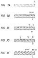
- Such an electrical connecting member is manufactured by a process as shown in Figures 3A to 3E of the accompanying drawings.
- Figures 3A to 3E are schematic cross-sectional views showing the essential steps of a method of manufacturing the electrical connecting member according to the prior art.
- a metal sheet 51 which provides a base body is first prepared (Figure 3A), and negative-type photosensitive resin 52 constituting the holding member 42 is applied onto the metal sheet 51 by a spinner and is pre-baked ( Figure 3B).
- Light is applied to the photosensitive resin 52 through a photomask (not shown) which forms a predetermined pattern to thereby expose the photosensitive resin 52 to the light, and development is effected (Figure 3C).
- the photosensitive resin 52 remains on the exposed portion, and in the unexposed portion, the photosensitive resin 52 is removed by the developing process, and apertures 53 in which the surface of the metal sheet is exposed on the bottom are formed. Temperature is increased to thereby effect the curing of the photosensitive resin 52, whereafter these are immersed in etching liquid to thereby each the surface of the metal sheet 51 exposed in the apertures 53, and recesses 54 are formed there ( Figure 3D).
- the apertures 53 and the recesses 54 are then filled with gold 55 constituting the electrically conductive members 54, and the electrically conductive members 45 are gold-plated so as to be protuberant to a predetermined height from the surface of the photosensitive resin 52, thereby forming bumps ( Figure 3E).
- the metal sheet 51 is removed by etching, whereby the electrical connecting member 41 in which the gold 55 and the photosensitive resin 52 constitute the electrically conductive members 45 and the holding member 42, respectively, as shown in Figure 2 is manufactured.
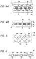
- Figure 4A of the accompanying drawings is a schematic view showing electric circuit parts 61, 62 and the electrical connecting member 41 before they are connected together
- Figure 4B of the accompanying drawings is a schematic view showing the electric circuit parts 61, 62 and the electrical connecting member 41 after they are connected together.
- the electric circuit parts 61 and 62 are these of a printed substrate or the like which are to be connected together.
- One electric circuit part 61 is opposed to that side of the electrical connecting member 41 on which one end 45a of each electrically conductive member 45 is exposed
- the other electric circuit part 62 is opposed to that side of the electrical connecting member 41 on which the other end 45b of each electrically conductive member 45 is exposed ( Figure 4A).
- the connecting portions 66 and 67 of the electric circuit parts 61 and 62, respectively, and the ends 45a and 45b of the electrically conductive members 45 are brought into pressure contact with each other while being heated and are made into an alloy, whereby they are connected together.
- the holding member 42 of polyimide resin or the like still remains around the electrically conductive members 45 after the connection. Accordingly, there is the problem that if a temperature change occurs after the connection and the holding member 42 is thermally expanded, strong stress will be imparted to the electrically conductive members 45 by the expanded holding member 42, whereby the electrically conductive members 45 may be damaged or severed.
- the concentration of stress may be caused in the electrically conductive members 45 and the joint portions of these to electrodes 40, 50 by the actions of the forces in the other directions than the direction of pressure contact during the pressure contact of the electrodes 40, 50 and the action of the thermal stress after the connection, and in such case, there is the problem that cracks occur in the electrically conductive members 45, said joint portions and further the holding member 42 and when the concentration of heavy stress occurs, the electrically conductive members 45 or the holding member 42 may be fractured to cause an increase in electrical resistance and unsatisfactory conduction.
- Figure 1 is a plan view of an electrical connecting member according to the prior art.
- Figure 2 is a schematic cross-sectional view of the electrical connecting member according to the prior art.
- Figures 3A to 3E are schematic cross-sectional views showing the essential steps of manufacturing the electrical connecting member according to the prior art.
- Figures 4A and 4B are illustrations showing the popular mode of use of the electrical connecting member.
- Figure 5 is a fragmentary plan view showing an electrical connecting member according to a first embodiment of the present invention.
- Figure 6 is a cross-sectional view taken along the line I - I of Figure 5.
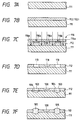
- Figures 7A to 7F are schematic cross-sectional views showing the essential steps of manufacturing the electrical connecting member according to the first embodiment of the present invention.
- Figures 8A to 8E are schematic cross-sectional views showing the steps of a method of manufacturing an electrical connecting member according to a second embodiment of the present invention.
- Figure 9 is a fragmentary plan view of an electrical connecting member according to a third embodiment of the present invention.
- Figure 10 is a cross-sectional view taken along the line II - II of Figure 9.
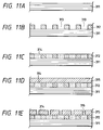
- Figures 11A to 11E are schematic cross-sectional views showing the essential steps of manufacturing the electrical connecting member according to the third embodiment of the present invention.
- Figures 12A to 12E are schematic cross-sectional views showing the essential steps of manufacturing the electrical connecting member according to the third embodiment of the present invention.
- Figures 13A and 13B are schematic cross-sectional views showing the essential steps of manufacturing the electrical connecting member according to the third embodiment of the present invention.
- Figure 14 is a plan view of an electrical connecting member according to a fourth embodiment of the present invention.
- Figure 5 is a fragmentary plan view of an electrical connecting member according to a first embodiment of the present invention
- Figure 6 is an enlarged longitudinal sectional view taken along the line I - I of Figure 5.
- the reference numeral 102 designates a holding member formed of photosensitive resin such as photosensitive polyimide resin.
- This holding member 102 has electrically conductive members 105 of gold or the like provided in an insulated state in a plurality of through-apertures 103 formed at predetermined intervals in the longitudinal and lateral directions thereof, and concave holes 108 are formed in the holding member 102 between the electrically conductive members 105.
- Each electrically conductive member 105 extends through the holding member 102, and one end thereof is slightly protruded and exposed on one surface of the holding member 102 and the other end thereof is slightly protruded and exposed on the other surface of the holding member 102. Also, each concave hole 108 is formed in the substantially central portion between adjacent electrically conductive members 105.
- each concave hole 108 The size, depth, cross-sectional shape and shape as viewed in a plan view of each concave hole 108 are not particularly restricted, but may be any ones which can absorb the dilation of the holding member 102 attributable to the difference in thermal expansion between the holding member 102 and the electrically conductive members 105 and mitigate or eliminate stress acting on the electrically conductive members 105.
- Figures 7A to 7F are schematic cross-sectional views showing the essential steps of manufacturing the electrical connecting member according to the present embodiment.
- a copper plate 111 having tungsten (W) film formed in layers on the surface thereof is first prepared ( Figure 7A), resist 112 for constituting the holding member 102 is applied onto the copper plate 111 and is pre-baked (Figure 7B), whereafter this is exposed to light ( Figure 7C).
- a mask 116 for use during this exposure use is made of a mask having 100 % light intercepting areas 116b which are formed of Cr film or the like and light attenuating areas 116c which use a Cr or ND filter formed on one surface of a mask base material 116a.
- the resist 112 in the portions opposed to the light intercepting areas 116b of the mask 116 is not exposed to the light and the resist 112 in the portions opposed to the light attenuating areas 116c is exposed to the light to a depth corresponding to the amount of light attenuation, and the other portions are light transmitting areas and are exposed to the light.
- apertures 103 through which the W film on the surface of the copper plate 111 is exposed at the bottom are formed in the portions opposed to the light intercepting areas 116b and concave holes 108 are formed in the portions opposed to the light attenuating areas 116c ( Figure 7D).
- the copper plate 111 is selectively etched to remove it, whereby there is obtained the electrical connecting member 101 as shown in Figure 6.
- one or more concave holes are formed in the holding member in which the electrically conductive members are provided and therefore, the stress the material of the holding member gives to the electrically conductive members by being expanded out toward the interior of the hole or holes when the temperature of the holding member becomes high enough to cause the thermal expansion of the holding member is mitigated and the damage or fracture of the electrically conductive members can be reliably prevented and further, when as shown in Figure 4, the electrically conductive members of the electrical connecting member and the connecting portions of other electric circuit parts are brought into pressure contact with each other, the force applied to the holding member through the electrically conductive members is effectively dispersed, whereby connection can be accomplished by low pressure and thus, the present embodiment achieves an excellent effect.
- FIGS 8A to 8E are schematic cross-sectional views showing the steps of manufacturing a second embodiment of the present invention.
- Negative type polyimide resin 202 which is photosensitive resin is first applied onto a copper plate 201 which is a base body by a spin coater and is pre-baked, whereafter light (not shown) is applied thereto through a photomask 203 forming a predetermined pattern, whereby the polyimide resin 202 is exposed to the light ( Figure 8A).
- the film thickness of the polyimide resin 202 applied is made greater than the desired film thickness of the holding member in an electrical connecting member to be manufactured, with a decrease by curing and shrinkage taken into account.
- the light intercepting pattern of the photomask 203 will be described here.
- the light intercepting pattern of the photomask 203 is comprised of first light intercepting portions 203a each having a diameter D and second light intercepting portions 203b each having a diameter d(LD).
- the diameter D is set so that openings can be formed in the polyimide resin 202 having a film thickness t
- the diameter d is set so that openings cannot be formed in the polyimide resin 202.
- the polyimide resin 202 remains on the portions exposed to the light, and the polyimide resin 202 is removed from the portions not exposed to the light by the developing process.
- Apertures 204 which reach the copper plate 201 are formed in the portions shielded from the light by the first light intercepting portions 203a, and recesses 205 which do not reach the copper plate 201 are formed in the portions shielded from the light by the second light intercepting portions 203b ( Figure 8B).
- the film thickness t of the polyimide resin 202 is 9 - 10 ⁇ m
- the exposure amount is 750 mJ/cm2
- the development conditions are such that the injection development time is 6 minutes and the injection rinse time is 1 minute.
- the diameter of the recesses is 8 ⁇ m
- the depth thereof is 6 ⁇ m
- the diameter of the recesses is 6 ⁇ m
- the depth thereof is 3 ⁇ m.
- the curing of the polyimide resin 202 is effected, whereafter the copper plate 201 is immersed in etching liquid to etch the copper plate 201, whereby the portions of the copper plate 201 which are near the apertures 204 are removed by etching and recesses 206 communicating with the apertures 204 are formed in the copper plate 201 ( Figure 8C).
- the diameter of the recesses 206 formed at this time is larger than the diameter of the apertures 204 and smaller than a half of the distance to the outer periphery of the adjacent aperture 204.
- the apertures 204 and the recesses 206 are filled with gold 207 by gold plating used with the copper plate 201 as a common electrode, and the gold plating is continued until the gold 207 protrudes from the surface of the polyimide resin 202 ( Figure 8D).
- the copper plate 201 is removed by metal etching by the use of etching liquid which etches copper but does not etch gold and polyimide resin, whereby an electrical connecting member 211 is manufactured ( Figure 8E).
- the gold 207 constitutes electrically conductive members 214 and the polyimide resin 202 constitutes a holding member 215, and a plurality of recesses 205 are provided in the surface of the holding member 215.
- the size and formation pitch of the electrically conductive members 214 in the thus manufactured electrical connecting member 211 are the same as those in the prior art.
- the number, diameter and depth of the recesses 205 formed between adjacent apertures 204 shown in the above-described manufacturing process are merely examples and of course, these may be set arbitrarily.
- the exposure process of the photosensitive resin is carried out by the use of the photomask having the first light intercepting portions and the second light intercepting portions differing in diameter from each other and therefore, a plurality of recesses can be easily formed in the photosensitive resin after the developing step, and there can be manufactured an electrical connecting member having recesses for absorbing the thermal expansion of the holding member provided in the holding member, and there can be provided an electrical connecting member which is high in the reliability when electric circuit parts are electrically connected together, and thus, the present embodiment achieves an excellent effect.
- Figure 9 is a fragmentary plan view of an electrical connecting member according to a third embodiment of the present invention
- Figure 10 is a longitudinal sectional view taken along the line II - II of Figure 9.
- the reference numeral 302 designates a holding member formed of polyimide film or the like.
- This holding member 302 has electrically conductive members 305 provided in a mutually insulated state in a plurality of apertures 303 formed at predetermined intervals in the longitudinal and lateral directions of the holding member, and a plurality of through-holes 308 are formed in the holding member 302 between the electrically conductive member 305.
- Each electrically conductive member 305 extends through the holding member 302, and one end thereof is slightly protruded and exposed on one surface of the holding member 302 and the other end thereof is slightly protruded and exposed on the other surface of the holding member 302.
- Each through hole 308 is formed in the substantially central portion between adjacent electrically conductive members 305.
- each through-hole 308 The size, cross-sectional shape and shape as viewed in a plan view of each through-hole 308 are not particularly restricted, but may be any ones which can absorb the dilation of the holding member 302 attributable to the difference in thermal expansion between the holding member 302 and the electrically conductive members 305 and can mitigate or eliminate stress acting on the electrically conductive members 305.
- FIGS 11A to 11E, 12A to 12E, 13A and 13B are schematic cross-sectional views showing the essential steps of manufacturing the electrical connecting member according to the present embodiment.
- a copper plate 311 comprising, for example, tungsten (W) film formed in layers on the surface thereof is prepared as a base body ( Figure 11A), and resist 312 is applied onto this copper plate 311 and pre-baked, whereafter exposure and development are effected to thereby form apertures 313 in which the W film on the surface of the copper plate 311 is exposed at the bottom, and the resist 312 is hard-pre-baked (Figure 11B).
- W tungsten
- Each aperture 313 is filled, for example, with gold 314 which is the electrically conductive member with the copper plate 311 as an electrode and gold plating is applied until the surface of the gold 314 becomes flush with the surface of the resist 312 ( Figure 11C), and photosensitive resin 315 forming the insulative holding member, for example, polyimide resin, is applied to the surface of the resist 312 and the surface of the gold 314 to a uniform thickness and is pre-baked (Figure 11D).
- gold 314 is the electrically conductive member with the copper plate 311 as an electrode and gold plating is applied until the surface of the gold 314 becomes flush with the surface of the resist 312
- photosensitive resin 315 forming the insulative holding member for example, polyimide resin
- the photosensitive resin 315 is exposed to light and developed to thereby form apertures 316 which are smaller than the diameter of the gold 314 and in which the surface of the gold 314 is exposed at the bottom in the substantially central portions of locations corresponding to the gold 314 ( Figure 11E), and pre-baking is effected to cure the photosensitive resin 315.
- each aperture 316 is filled, for example, with gold 317 which is an electrically conductive member and gold plating is applied until the surface of the gold 317 becomes flush with the surface of the photosensitive resin 315 ( Figure 12A), and resist 318 is applied uniformly to the surface of the photosensitive resin 315 and the surface of the gold 317 and is pre-baked, whereafter exposure and development are effected to thereby form apertures 319 which are substantially equal in size to the diameter of the gold 314 and in which the gold 317 and part of the photosensitive resin 315 are exposed at the bottom at locations corresponding to the gold 317 ( Figure 12B).
- each aperture is filled with gold 320 which is an electrically conductive member and gold plating is applied until the surface of the gold 320 becomes flush with the surface of the resist 318 ( Figure 12C).
- the copper plate 301 is first selectively etched to remove it (Figure 12D), and then the pre-baked resist 312 is removed by ashing using O2 plasma ( Figure 12E), and the resist 318 is removed by resist removing liquid ( Figure 13A).
- the resist 318 may be first removed by the use of resist removing liquid, whereafter the copper plate 311 may be etched and the resist 312 may be removed by ashing using O2 plasma. Subsequently, a high energy beam is projected onto the photosensitive resin 315 in the portions wherein the electrically conductive members are absent by the use of a mask 321 ( Figure 13B), whereby the through-holes 308 as shown in Figures 9 and 10 are formed there, whereby there is manufactured an electrical connecting member in which the gold 314, 317, 320 constitutes the electrically conductive material 305 and the photosensitive resin 315 constitutes the holding member 302. Concave holes may simply be provided instead of the through-holes 308.
- bump has its expanse in the lateral direction restricted by the apertures 313 and 319 formed in the resists 312 and 318 and thus, a convenience such as the contact of adjacent electrically conductive members with each other can be prevented, and by suitably setting the thicknesses of the regists 312 and 318, it becomes possible to set the height of protrusion of the electrically conductive members from the holding member arbitrarily.
- one or more holes are formed in the holding member in which the electrically conductive members are provided and therefore, when the temperature of the holding member becomes high and the holding member is thermally expanded, the material of the holding member swells out toward the interior of the holes and therefore the stress given to the electrically conductive members is liberated, whereby the damage or fracture of the electrically conductive members can be reliably prevented and further, the force applied to the holding member through the electrically conductive members is effectively dispersed and the connection of the connecting member can be accomplished by low pressure and thus, the present embodiment achieves an excellent effect.
- electrically conductive members on the surface of a holding member are disposed in a staggered fashion to thereby achieve an arrangement of higher density than in the case where they are disposed in longitudinal and lateral rows, whereby the number of electrically conductive members joined to the electrodes of electric circuit parts is increased and the degree of concentration of stress in the electrically conductive members is alleviated to thereby prevent the accurrence of the crack or fracture of the holding member and eliminate the problems of an increase in electrical resistance and unsatisfactory conduction when the electric circuit parts are connected together.
- the lower limit of the diameter of each electrically conductive member 403 is of the order of 10 ⁇ m and the lower limit of the P dimensions when the electrically conductive members 402 is of the order of 20 ⁇ m.
- the electrical connecting member 401 according to the present embodiment has a construction similar to that of the prior art shown in Figure 2, and the connection of electric circuit parts by the electrical connecting member 401 according to the present embodiment is also effected just in the same manner as in the prior art as shown in Figure 4.
- the feature of the electrical connecting member 401 according to the present embodiment is that as is clear from the plan view of Figure 14, the electrically conductive members 403 on the surface of the holding member 402, unlike those in the prior art, are disposed in a staggered fashion.
- Figure 14 and Figure 1 which shows the arrangement of the prior-art electrically conductive members 45, the portions of the holding members having substantially equal areas are cut out and the diametrical dimensions of the electrically conductive members and the intervals (P dimensions) between the electrically conductive members are shown as being substantially equal.
- the number of the electrically conductive members appearing in the figure is 20, whereas in Figure 14, the number of the electrically conductive members completely contained in the figure is 23 and the number of the electrically conductive members incompletely contained in the figure is 4 and thus, 27 electrically conductive members 403 in total appear in the figure.
- the diametrical dimensions of the electrically conductive members 403 are determined by the formation accuracy of the pattern on the photomask used during the exposure of polyimide resin 411 in the aforedescribed manufacturing process, and the aforementioned P dimensions are determined from the viewpoint of the maintenance of the insulated state between adjacnet electrically conductive members 403, and these conditions are invariable irrespective of the mode of arrangement of the electrically conductive members 403. Accordingly, in the electrical connecting member 401 according to the present embodiment, the arrangement of the electrically conductive members 403 at greatly higher density than in the prior art becomes possible.
- electrodes 440, 450 which are the objects of connection are shown as the same dimensions as in Figure 1.
- the electrodes 40, 50 can contact with only six electrically conductive members 45 at most, including incomplete ones, whereas in Figure 14, substantially complete contact with as many as seven electrically conductive members 403 takes place.
- the degree of concentration of stress in the respective electrically conductive members 403 is alleviated and the possibility of crack or fracture occurring in the electrically conductive members 403 and the holding member 402 during the pressure contact of the electrodes 440, 450 is reduced, and the problems of the resultant increase in electrical resistance and unsatisfactory conduction are effectively eliminated.
- connection when connection is effected normally, electrical conduction takes place through a greater number of electrically conductive members 403 in the electrical connecting member 401 according to the present embodiment than in the prior art and therefore, the electrical resistance in the connected portions is reduced and a good conductive state is obtained.
- the electrically conductive members are disposed in a staggered fashion on the surface of the holding member and therefore, the number of electrically conductive members disposed per unit area can be greatly increased as compared with the prior art, and during the pressure contact of electric circuit parts, the degree of concentration of stress in each electrically conductive member is alleviated and the possibility of the occurrence of an increase in electrical resistance and unsatisfactory conduction attributable to crack or fracture caused in the electrically condutive members and the holding member is effectively eliminated and thus, the present embodiment achieves an excellent effect.
- conductive members such as Mo and Ni may be heated and alloyed, or use may be made of a high melting point metal which does not produce a metal-to-metal compound with gold which is electrically conductive members.
- photosensitive polyimide resin as the holding member which is an electrically insulative material
- photosensitive resin thermosetting resin or film thereof, other insulative epoxy resins, silicone resin or film of these.
- an inorganic material, a metal material and an alloy material which are in a desired form such as powder, fiber, a plate-like body, a bar-like body or a spherical body may be dispersed and contained in these resins.
- metal material and alloy material contained mention may be made of Au, Ag, Cu, Al, Be, Ca, Mg, Mo, Fe, Ni, Co, Mn, W, Cr, Nb, Zr, Ti, Ta, Zn, Sn, Pb-Sn or the like, and as the inorganic material contained, mention may be made of ceramics such as SiO2, B2O3, Al2O3, Na2O, K2O, CaO, ZnO, BaO, PbO, Sb2O3, As2O3, La2O3, ZrO2, P2O5, TiO2, MgO, SiC, BeO, BP, BN, AlN, B4C, TaC, TiB2, CrB2, TiN, Si3N4 or Ta2O5, diamond, glass, carbon, boron or the like.
- ceramics such as SiO2, B2O3, Al2O3, Na2O, K2O, CaO, ZnO, BaO, PbO, Sb2O3, As2O3, La2O3, ZrO2,
- Co2, YAG, N2, Ar or Kr laser beam may be used instead of the excimer laser beam.
- an ion beam of FIBE, IBE, sputter or the like may be used instead of the laser beam.
- gold is used as the material of the electrically conductive members, but alternatively, use may be made of a metal such as Cu, Ag, Be, Ca, Mg, Mo, Ni, W, Fe, Ti, In, Ta, Zn, Al, Sn or Pb-Sn or an alloy of these.
- the cross-sectional shape of the electrically conductive members may be circular, square or other shape, but to avoid the excessive concentration of stress, shapes having no angles are desirable.
- the electrically conductive members are not limited to gold, but any other electrically conductive metal or conductive alloy may also be used.
- polyimide resin is used as photosensitive resin which provides the holding member, but other any photosensitive resin such as epoxy resin or silicone resin may also be used.
- a copper plate is used as the base body, whereas this is not restrictive, but other metal or alloy may be used.
- the material of the electrically conductive members and the material of the base body be made different from each other.
- the electrically conductive members need not be vertically disposed in the holding member, but may be oblique from one surface side to the other surface side of the holding member.
- an electrical connecting member capable of well connecting electric circuit parts together and a method of manufacturing the same.
- An electrical connecting member having a holding member formed of an electrically insulative material, and a plurality of electrically conductive members provided in a mutually insulated state in the holding member, one end of each of the electrically conductive members being exposed on one surface of the holding member and the other end of each of the electrically conductive members being exposed on the other surface of the holding member is characterized in that one or more concave holes are formed in the holding member.
Landscapes
- Manufacturing Of Electrical Connectors (AREA)
- Coupling Device And Connection With Printed Circuit (AREA)
- Multi-Conductor Connections (AREA)
Applications Claiming Priority (12)
| Application Number | Priority Date | Filing Date | Title |
|---|---|---|---|
| JP5390491A JPH04269476A (ja) | 1991-02-25 | 1991-02-25 | 電気的接続部材 |
| JP5390491 | 1991-02-25 | ||
| JP5390691A JPH04269477A (ja) | 1991-02-25 | 1991-02-25 | 電気的接続部材 |
| JP53904/91 | 1991-02-25 | ||
| JP5390691 | 1991-02-25 | ||
| JP53906/91 | 1991-02-25 | ||
| JP6909191 | 1991-03-09 | ||
| JP69092/91 | 1991-03-09 | ||
| JP03069092A JP3101883B2 (ja) | 1991-03-09 | 1991-03-09 | 電気的接続部材及びその製造方法 |
| JP6909291 | 1991-03-09 | ||
| JP6909191A JPH0645400A (ja) | 1991-03-09 | 1991-03-09 | 電気的接続部材の製造方法 |
| JP69091/91 | 1991-03-09 |
Publications (2)
| Publication Number | Publication Date |
|---|---|
| EP0501357A1 true EP0501357A1 (fr) | 1992-09-02 |
| EP0501357B1 EP0501357B1 (fr) | 2003-06-04 |
Family
ID=27462979
Family Applications (1)
| Application Number | Title | Priority Date | Filing Date |
|---|---|---|---|
| EP92103024A Expired - Lifetime EP0501357B1 (fr) | 1991-02-25 | 1992-02-24 | Pièce de connexion électrique et son procédé de fabrication |
Country Status (3)
| Country | Link |
|---|---|
| US (1) | US5600884A (fr) |
| EP (1) | EP0501357B1 (fr) |
| DE (1) | DE69233088T2 (fr) |
Cited By (2)
| Publication number | Priority date | Publication date | Assignee | Title |
|---|---|---|---|---|
| WO2002015653A1 (fr) * | 2000-08-10 | 2002-02-21 | 3M Innovative Properties Company | Ensemble d'interconnexion flexible |
| WO2002037565A3 (fr) * | 2000-11-06 | 2003-04-24 | Mcnc | Procede permettant de connecter des conducteurs sur differents niveaux d'un dispositif microelectronique et appareil associe |
Families Citing this family (21)
| Publication number | Priority date | Publication date | Assignee | Title |
|---|---|---|---|---|
| EP0805493B1 (fr) | 1991-02-22 | 2007-02-28 | Canon Kabushiki Kaisha | Corps d'interconnexion électrique et procédé de fabrication |
| KR0146063B1 (ko) * | 1995-03-28 | 1998-08-01 | 문정환 | 반도체 패키지 및 그 제조방법 |
| JP3376218B2 (ja) * | 1996-08-30 | 2003-02-10 | キヤノン株式会社 | 回路基板接続装置 |
| US6904675B1 (en) | 1996-09-27 | 2005-06-14 | Hewlett-Packard Development, L.P. | Method of forming electrical interconnects having electromigration-inhibiting plugs |
| US6245996B1 (en) | 1996-09-27 | 2001-06-12 | Compaq Computer Corporation | Electrical interconnect structure having electromigration-inhibiting segments |
| US6400018B2 (en) | 1998-08-27 | 2002-06-04 | 3M Innovative Properties Company | Via plug adapter |
| US6291776B1 (en) | 1998-11-03 | 2001-09-18 | International Business Machines Corporation | Thermal deformation management for chip carriers |
| JP3162677B2 (ja) * | 1998-12-10 | 2001-05-08 | 株式会社双晶テック | 多点導電シート |
| TW396462B (en) * | 1998-12-17 | 2000-07-01 | Eriston Technologies Pte Ltd | Bumpless flip chip assembly with solder via |
| US6462414B1 (en) * | 1999-03-05 | 2002-10-08 | Altera Corporation | Integrated circuit package utilizing a conductive structure for interlocking a conductive ball to a ball pad |
| US6402970B1 (en) * | 2000-08-22 | 2002-06-11 | Charles W. C. Lin | Method of making a support circuit for a semiconductor chip assembly |
| US6350386B1 (en) * | 2000-09-20 | 2002-02-26 | Charles W. C. Lin | Method of making a support circuit with a tapered through-hole for a semiconductor chip assembly |
| TWI236329B (en) * | 2003-12-25 | 2005-07-11 | Au Optronics Corp | Printed circuit board of display for preventing accumulation of thermal expansion |
| US7446399B1 (en) | 2004-08-04 | 2008-11-04 | Altera Corporation | Pad structures to improve board-level reliability of solder-on-pad BGA structures |
| JP2007005246A (ja) * | 2005-06-27 | 2007-01-11 | Sumitomo Electric Ind Ltd | 多孔質樹脂基材及び多層基板 |
| JP2007030465A (ja) * | 2005-07-29 | 2007-02-08 | Fujifilm Holdings Corp | 基板の製造方法、液体吐出ヘッドの製造方法、液体吐出ヘッド及び画像形成装置 |
| US7595999B2 (en) * | 2007-06-21 | 2009-09-29 | Dell Products L.P. | System and method for coupling an integrated circuit to a circuit board |
| US8618647B2 (en) * | 2011-08-01 | 2013-12-31 | Tessera, Inc. | Packaged microelectronic elements having blind vias for heat dissipation |
| US20130113118A1 (en) * | 2011-11-04 | 2013-05-09 | Stats Chippac, Ltd. | Semiconductor Device and Method of Forming Sloped Surface in Patterning Layer to Separate Bumps of Semiconductor Die from Patterning Layer |
| US11637406B2 (en) * | 2017-05-18 | 2023-04-25 | Shin-Etsu Polymer Co., Ltd. | Electrical connector and method for producing same |
| IT201700073501A1 (it) * | 2017-06-30 | 2018-12-30 | St Microelectronics Srl | Prodotto a semiconduttore e corrispondente procedimento |
Citations (6)
| Publication number | Priority date | Publication date | Assignee | Title |
|---|---|---|---|---|
| US4067945A (en) * | 1976-03-24 | 1978-01-10 | Essex International, Inc. | Method of making a multi-circuit electrical interconnector |
| US4231811A (en) * | 1979-09-13 | 1980-11-04 | Intel Corporation | Variable thickness self-aligned photoresist process |
| FR2519228A1 (fr) * | 1981-12-29 | 1983-07-01 | Inst Kolloidnoi Khim | Connecteur electrique |
| EP0344720A2 (fr) * | 1988-05-31 | 1989-12-06 | Canon Kabushiki Kaisha | Procédé pour la fabrication de pièces de connexion électriques |
| EP0368262A2 (fr) * | 1988-11-09 | 1990-05-16 | Nitto Denko Corporation | Substrat à conducteurs, bande de support, dispositif semi-conducteur utilisant la bande de support, et structure de montage comprenant le dispositif semi-conducteur |
| EP0425316A2 (fr) * | 1989-10-27 | 1991-05-02 | International Business Machines Corporation | Connecteur électrique |
Family Cites Families (7)
| Publication number | Priority date | Publication date | Assignee | Title |
|---|---|---|---|---|
| US3193789A (en) * | 1962-08-01 | 1965-07-06 | Sperry Rand Corp | Electrical circuitry |
| US4766371A (en) * | 1982-07-24 | 1988-08-23 | Risho Kogyo Co., Ltd. | Test board for semiconductor packages |
| US4641222A (en) * | 1984-05-29 | 1987-02-03 | Motorola, Inc. | Mounting system for stress relief in surface mounted components |
| US5013249A (en) * | 1986-06-19 | 1991-05-07 | Labinal Components And Systems, Inc. | Electrical connectors |
| EP0349756A3 (fr) * | 1988-05-30 | 1991-03-20 | Canon Kabushiki Kaisha | Méthode de fabrication de dispositif de circuit électrique |
| US4991290A (en) * | 1988-07-21 | 1991-02-12 | Microelectronics And Computer Technology | Flexible electrical interconnect and method of making |
| US5155302A (en) * | 1991-06-24 | 1992-10-13 | At&T Bell Laboratories | Electronic device interconnection techniques |
-
1992
- 1992-02-24 DE DE69233088T patent/DE69233088T2/de not_active Expired - Fee Related
- 1992-02-24 EP EP92103024A patent/EP0501357B1/fr not_active Expired - Lifetime
-
1993
- 1993-12-22 US US08/171,862 patent/US5600884A/en not_active Expired - Lifetime
Patent Citations (6)
| Publication number | Priority date | Publication date | Assignee | Title |
|---|---|---|---|---|
| US4067945A (en) * | 1976-03-24 | 1978-01-10 | Essex International, Inc. | Method of making a multi-circuit electrical interconnector |
| US4231811A (en) * | 1979-09-13 | 1980-11-04 | Intel Corporation | Variable thickness self-aligned photoresist process |
| FR2519228A1 (fr) * | 1981-12-29 | 1983-07-01 | Inst Kolloidnoi Khim | Connecteur electrique |
| EP0344720A2 (fr) * | 1988-05-31 | 1989-12-06 | Canon Kabushiki Kaisha | Procédé pour la fabrication de pièces de connexion électriques |
| EP0368262A2 (fr) * | 1988-11-09 | 1990-05-16 | Nitto Denko Corporation | Substrat à conducteurs, bande de support, dispositif semi-conducteur utilisant la bande de support, et structure de montage comprenant le dispositif semi-conducteur |
| EP0425316A2 (fr) * | 1989-10-27 | 1991-05-02 | International Business Machines Corporation | Connecteur électrique |
Cited By (3)
| Publication number | Priority date | Publication date | Assignee | Title |
|---|---|---|---|---|
| US6524115B1 (en) | 1999-08-20 | 2003-02-25 | 3M Innovative Properties Company | Compliant interconnect assembly |
| WO2002015653A1 (fr) * | 2000-08-10 | 2002-02-21 | 3M Innovative Properties Company | Ensemble d'interconnexion flexible |
| WO2002037565A3 (fr) * | 2000-11-06 | 2003-04-24 | Mcnc | Procede permettant de connecter des conducteurs sur differents niveaux d'un dispositif microelectronique et appareil associe |
Also Published As
| Publication number | Publication date |
|---|---|
| US5600884A (en) | 1997-02-11 |
| DE69233088T2 (de) | 2003-12-24 |
| DE69233088D1 (de) | 2003-07-10 |
| EP0501357B1 (fr) | 2003-06-04 |
Similar Documents
| Publication | Publication Date | Title |
|---|---|---|
| US5600884A (en) | Method of manufacturing electrical connecting member | |
| EP0504614B1 (fr) | Corps d'interconnexion électrique et procédé de sa fabrication | |
| US7129579B2 (en) | Semiconductor apparatus and method for fabricating the same | |
| DE68928633T2 (de) | Verfahren zur Herstellung elektrischer Verbindungsteile | |
| EP0229850B1 (fr) | Bornes de connection entre des substrats et procede de production | |
| US5174766A (en) | Electrical connecting member and electric circuit member | |
| EP0177042B1 (fr) | Dispositif de circuit semi-conducteur et son procédé de fabrication | |
| DE10164494B4 (de) | Verkapseltes Bauelement mit geringer Bauhöhe sowie Verfahren zur Herstellung | |
| US5379515A (en) | Process for preparing electrical connecting member | |
| US5069628A (en) | Flexible electrical cable connector with double sided dots | |
| US6100175A (en) | Method and apparatus for aligning and attaching balls to a substrate | |
| JPH06283571A (ja) | 集積回路と基板との相互接続構造及びその製造方法 | |
| EP0206337A2 (fr) | Substrat pour des connexions multicouches comprenant des plages de câblage de rechange | |
| EP0445759A1 (fr) | Structures multicouches avec interconnexion des couches | |
| EP0631313B1 (fr) | Dispositif semi-conducteur comprenant une traversée | |
| EP0987749A2 (fr) | Dispositif semiconducteur, sa structure d'électrode et son procédé de fabrication | |
| US6309910B1 (en) | Microelectronic components with frangible lead sections | |
| JP2909639B2 (ja) | 電気的接続部材の製造方法 | |
| JP3057206B2 (ja) | 電気的接続部材及びその製造方法 | |
| JP2909640B2 (ja) | 電気的接続部材の製造方法 | |
| JP3038361B2 (ja) | 電気的接続部材の製造方法 | |
| JPH04282578A (ja) | 電気的接続部材及びその製造方法 | |
| JP2796872B2 (ja) | 電気的接続部材の製造方法 | |
| JP2516440B2 (ja) | 電気的接続部材の製造方法 | |
| JP2000294585A (ja) | バンプ構造及びその形成方法 |
Legal Events
| Date | Code | Title | Description |
|---|---|---|---|
| PUAI | Public reference made under article 153(3) epc to a published international application that has entered the european phase |
Free format text: ORIGINAL CODE: 0009012 |
|
| AK | Designated contracting states |
Kind code of ref document: A1 Designated state(s): DE FR GB IT NL |
|
| 17P | Request for examination filed |
Effective date: 19930119 |
|
| 17Q | First examination report despatched |
Effective date: 19951011 |
|
| GRAG | Despatch of communication of intention to grant |
Free format text: ORIGINAL CODE: EPIDOS AGRA |
|
| GRAG | Despatch of communication of intention to grant |
Free format text: ORIGINAL CODE: EPIDOS AGRA |
|
| GRAH | Despatch of communication of intention to grant a patent |
Free format text: ORIGINAL CODE: EPIDOS IGRA |
|
| GRAH | Despatch of communication of intention to grant a patent |
Free format text: ORIGINAL CODE: EPIDOS IGRA |
|
| GRAA | (expected) grant |
Free format text: ORIGINAL CODE: 0009210 |
|
| AK | Designated contracting states |
Designated state(s): DE FR GB IT NL |
|
| PG25 | Lapsed in a contracting state [announced via postgrant information from national office to epo] |
Ref country code: IT Free format text: LAPSE BECAUSE OF FAILURE TO SUBMIT A TRANSLATION OF THE DESCRIPTION OR TO PAY THE FEE WITHIN THE PRESCRIBED TIME-LIMIT;WARNING: LAPSES OF ITALIAN PATENTS WITH EFFECTIVE DATE BEFORE 2007 MAY HAVE OCCURRED AT ANY TIME BEFORE 2007. THE CORRECT EFFECTIVE DATE MAY BE DIFFERENT FROM THE ONE RECORDED. Effective date: 20030604 Ref country code: NL Free format text: LAPSE BECAUSE OF FAILURE TO SUBMIT A TRANSLATION OF THE DESCRIPTION OR TO PAY THE FEE WITHIN THE PRESCRIBED TIME-LIMIT Effective date: 20030604 Ref country code: FR Free format text: LAPSE BECAUSE OF FAILURE TO SUBMIT A TRANSLATION OF THE DESCRIPTION OR TO PAY THE FEE WITHIN THE PRESCRIBED TIME-LIMIT Effective date: 20030604 |
|
| REG | Reference to a national code |
Ref country code: GB Ref legal event code: FG4D |
|
| REF | Corresponds to: |
Ref document number: 69233088 Country of ref document: DE Date of ref document: 20030710 Kind code of ref document: P |
|
| NLV1 | Nl: lapsed or annulled due to failure to fulfill the requirements of art. 29p and 29m of the patents act | ||
| PLBE | No opposition filed within time limit |
Free format text: ORIGINAL CODE: 0009261 |
|
| STAA | Information on the status of an ep patent application or granted ep patent |
Free format text: STATUS: NO OPPOSITION FILED WITHIN TIME LIMIT |
|
| 26N | No opposition filed |
Effective date: 20040305 |
|
| EN | Fr: translation not filed | ||
| PGFP | Annual fee paid to national office [announced via postgrant information from national office to epo] |
Ref country code: DE Payment date: 20090228 Year of fee payment: 18 |
|
| PGFP | Annual fee paid to national office [announced via postgrant information from national office to epo] |
Ref country code: GB Payment date: 20090218 Year of fee payment: 18 |
|
| GBPC | Gb: european patent ceased through non-payment of renewal fee |
Effective date: 20100224 |
|
| PG25 | Lapsed in a contracting state [announced via postgrant information from national office to epo] |
Ref country code: DE Free format text: LAPSE BECAUSE OF NON-PAYMENT OF DUE FEES Effective date: 20100901 |
|
| PG25 | Lapsed in a contracting state [announced via postgrant information from national office to epo] |
Ref country code: GB Free format text: LAPSE BECAUSE OF NON-PAYMENT OF DUE FEES Effective date: 20100224 |