EP0502428A2 - Convertisseur analogique-numérique - Google Patents
Convertisseur analogique-numérique Download PDFInfo
- Publication number
- EP0502428A2 EP0502428A2 EP92103405A EP92103405A EP0502428A2 EP 0502428 A2 EP0502428 A2 EP 0502428A2 EP 92103405 A EP92103405 A EP 92103405A EP 92103405 A EP92103405 A EP 92103405A EP 0502428 A2 EP0502428 A2 EP 0502428A2
- Authority
- EP
- European Patent Office
- Prior art keywords
- conversion
- analog
- terminal
- request trigger
- digital conversion
- Prior art date
- Legal status (The legal status is an assumption and is not a legal conclusion. Google has not performed a legal analysis and makes no representation as to the accuracy of the status listed.)
- Withdrawn
Links
Images




Classifications
-
- H—ELECTRICITY
- H03—ELECTRONIC CIRCUITRY
- H03M—CODING; DECODING; CODE CONVERSION IN GENERAL
- H03M1/00—Analogue/digital conversion; Digital/analogue conversion
- H03M1/12—Analogue/digital converters
-
- H—ELECTRICITY
- H03—ELECTRONIC CIRCUITRY
- H03M—CODING; DECODING; CODE CONVERSION IN GENERAL
- H03M1/00—Analogue/digital conversion; Digital/analogue conversion
- H03M1/12—Analogue/digital converters
- H03M1/1205—Multiplexed conversion systems
- H03M1/121—Interleaved, i.e. using multiple converters or converter parts for one channel
- H03M1/1215—Interleaved, i.e. using multiple converters or converter parts for one channel using time-division multiplexing
-
- H—ELECTRICITY
- H03—ELECTRONIC CIRCUITRY
- H03M—CODING; DECODING; CODE CONVERSION IN GENERAL
- H03M1/00—Analogue/digital conversion; Digital/analogue conversion
- H03M1/12—Analogue/digital converters
- H03M1/1205—Multiplexed conversion systems
- H03M1/122—Shared using a single converter or a part thereof for multiple channels, e.g. a residue amplifier for multiple stages
- H03M1/1225—Shared using a single converter or a part thereof for multiple channels, e.g. a residue amplifier for multiple stages using time-division multiplexing
Definitions
- the present invention relate to a hardware arrangement of an analog/digital converter (hereinafter referred to as A/D converter), and more particularly to an operational sequence to be performed by the hardware.
- A/D converter an analog/digital converter
- the conventional A/D converter has, in general, an arrangement as shown in FIG. 1 where typical operational sequences are divided into the following two cases.
- a terminal required for A/D conversion is selected by a terminal selecting section 12-2 from a group of L pieces of analog input terminals 12-1.
- Voltage applied to the selected analog input terminal is supplied to an A/D conversion unit 12-4 through a switching section 12-3 for generation of an A/D conversion request trigger which is a signal to be generated by a request for starting A/D conversion or to be automatically generated in case any satisfactory condition has been established on the hardware.
- an A/D conversion request trigger is supplied to an A/D conversion request trigger control unit 12-5 to carry out a sequence control operation thereof for commencement of A/D conversion and after completion of the A/D conversion, the converted result is stored in a conversion result storage register 12-6.
- the converted result stored in the conversion result storage register 12-6 is read out by the software to terminate series of the works.
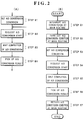
- FIG. 2 is a flowchart of a series of works by means of the software for executing the A/D conversion, in which the flow (A) is an A/D conversion process of the terminal selected by the terminal section 12-2.
- the flow (B) is the A/D conversion process of the terminal other than that selected by the terminal selecting section 12-2, which is read out and executed upon execution of the flow (A).
- the steps are processed, for example, by the step S3 to set the terminal intended to perform the A/D conversion in emergency for the commencement of the A/D conversion by means of S4.
- the stored value of the conversion result storage register 12-6 is read out at the in step S6 and the process is returned to the flow (A) through the returning a procedure of the step 7 as hereinbefore described.
- the explanation about the processing of result of the A/D conversion obtained at the flow (B) has been omitted.
- the conventional A/D converter entails many disadvantages as described hereinafter.
- the first one requires many processings with respect to the software with an obvious low speed of the processing and difficulty in performing the processing in emergency.
- the decision and the process with the software upon repeated execution of the A/D conversions, there are uneven times between the time where the A/D conversion is required and the time when the conversion value is actually obtained.
- a large amount of the processing is required with erroneous operations occurable upon programming.
- the processing for the software are a few. If, however, there are many analog input terminals to be A/D converted, an executing period of the A/D conversion processing of a particular terminal would be extended, so that a considerable time is required for the period from the instant where the A/D conversion is required to the instant where the conversion value is actually obtained with considerable evenness in times before the A/D conversion value is obtained.
- the foregoing disadvantages may be solved by the conventional techniques with two A/D converters in which one is used in an ordinary manner while the other usually placed under the standby condition is used only in emergency.
- the arrangement thus allows the A/D converter placed under the standby condition to response to the A/D conversion start request at a short time from the request.
- the arrangement intends to process separately a terminal which needs to obtain the A/D conversion value with a high priority and the other terminals free of such need, thereby to improve the responsibility and the time dispersion before the A/D conversion value is determined.
- the arrangement of the type described seems very convenient in use for the customers, notwithstanding a relatively larger scale is required for the A/D converter even with a single circuit. Preparation of the A/D converter of two circuits is therefore not practical on account of high cost.
- An A/D converter in accordance with the invention is comprised of a single A/D conversion unit, L pieces of analog input terminals, M pieces of terminal selecting sections for selecting one input terminal or a plurality of input terminals separately from the input terminal of L pieces, a switching section for switching terminals in accordance with the instructions from the terminal selecting sections of M pieces conversion result storage registers of M pieces for storing A/D convered request of analog voltage to be applied to analog input terminals selected by terminal selecting sections of M pieces, A/D conversion requested trigger input of M pieces, and a control unit for controlling an A/D conversion sequence.
- a value of M is equal to 2 and an operation of the block diagram is separated into the following four operations.
- a terminal to be A/D converted by the first A/D conversion request trigger and selected from a group of L pieces of analog input terminals 1-1 is set in the first terminal selecting section 1-2, while another terminal to be A/D converted by the second A/D conversion request trigger is set in the second terminal selecting section 1-3.
- the first terminal selecting section 1-2 is set with the terminal number 1
- the second terminal selecting section 1-3 is set with the terminal number 2.
- Conceivable means for generating an A/D conversion request trigger may be of a means for generating an A/D conversion start request by the software instruction or of a means for automatically generating by the hardware processing upon fulfillment of some available conditions. The present examples will be described hereinafter about generation of the A/D conversion request trigger by the instruction of software.
- a control unit 1-4 receives the first A/D conversion request trigger and instructs the switching section 1-5 to make the terminal selected by the first terminal selecting section 1-2 or the terminal number 1 effective for supplying a voltage applied to the terminal number 1 to the A/D conversion unit 1-6.
- the control unit 1-4 then instructs the A/D conversion unit 1-6 to start an execution of the A/D conversion. After completion of the A/D conversion, the control unit 1-4 instructs the first conversion result storage register 1-7 to renew the present storage value with the just completed A/D conversion value. At this time, the second conversion result storage register 1-8 holds a previous value without renewing any value. Finally, the A/D conversion value is red out to terminate the series of works.
- the control unit 1-4 receives the second A/D conversion request trigger and instructs the switching section 1-5 to make the terminal selected by the second terminal selecting section 1-3 or the terminal number 2 effective for supplying a voltage applied to the terminal number 2 to the A/D conversion unit 1-6.
- the control unit 1-4 then instructs the A/D conversion unit 1-6 to start an execution of the A/D conversion.
- the control unit 1-4 instructs the second conversion result storage register 1-8 to renew to the present storage value with the just completed A/D conversion value.
- the first conversion result storage register 1-7 holds a previous value without renewing any value.
- an operational sequence constitutes a feature of the invention.
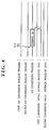
- the second A/D conversion request trigger is applied while the A/D conversion is executed by the the A/D conversion request trigger.
- settings of A/D conversion conditions such as setting of the first terminal selecting section 1-2, setting of the second terminal selecting section 1-3, and initial setting required for the other A/D conversion take place at the steps M1 and M2.
- the first A/D conversion request trigger is generated, and upon termination of execution of the A/D conversion at the step M4, the converted result of A/D conversion is pick up at the step M5.
- a call of the flow (B) is carried out by the branching process upon determination of fulfill of the predetermined conditions during execution of the flow (A) or by so called interrupting process.
- the calling of the flow (B) is assumed to be performed by the branching process through with a program when the predetermined conditions are fulfilled.
- the process is transferred to the flow (B) and when the A/D conversion of the terminal other than the terminal selected by the first terminal selecting section takes place, a terminal information to be A/D converted at the flow (A) is set to the first terminal selecting section, while the terminal information to be A/D converted at at the flow (B) is set to the second terminal selecting section.
- the control unit 1-4 operates to carry out a sequence control for interruption of the A/D conversion by the first A/D conversion request trigger and subsequent commencement of the A/D conversion by the second A/D conversion request trigger.
- an interrupt processing of the A/D conversion with the first A/D conversion request trigger may thus be omitted. Accordingly, just after the shift to the flow (B), a request for starting the A/D conversion may be delivered to a terminal selected by the second terminal selecting section 1-3, enabling to generate the second A/D conversion request trigger.
- the control unit 1-4 instructs the A/D conversion unit 1-6 to interrupt the A/D conversion under execution and in turn instructs the switching section 1-5 to make the terminal selected by the first terminal selecting section 1-2 or the terminal number 1 ineffective but to make another terminal selected by the second terminal selecting section 1-3 or the terminal number 2 effective.
- a voltage to be applied to the terminal number 2 may be supplied to the A/D conversion unit 1-6 and the control unit 1-4 instructs the A/D conversion unit 1-6 to start an execution of the A/D conversion.
- control unit 1-4 instructs the second conversion result storage register 1-8 to renew the present storage value by the just obtained A/D conversion value.
- A/D conversion by the first A/D conversion request trigger is interrupted so that the first conversion result storage register 1-7 is not renewed, storing the A/D conversion result of one step before.
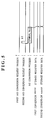
- the flowchart of FIG 7 shows such situation that the first A/D conversion request trigger m3 is given while the A/D conversion takes place by the second A/D conversion request trigger s3 where in case the first A/D conversion request trigger is periodically generated irrespective of the flow of the program, the third example processing hereinbefore described intervenes and before such processing terminates, the first A/D conversion request trigger is generated.
- the second A/D conversion request trigger is predominated than the first A/D conversion request trigger as one of the characteristic features of the invention, notwithstanding to obtain more perfect result, the A/D conversion processing with the second A/D conversion request trigger should preferably be continued to its completion.
- the control unit 1-4 is requested to have such function that any supply of the first A/D conversion request trigger should never be received during execution of the A/D conversion processing with the second A/D conversion request trigger.
- FIG. 3 Another embodiment of the invention will be described with reference to FIG. 3 wherein an operation is divided into four cases like the first embodiment, providing a value of M as 2. Operational timings are different from the first embodiment as shown in FIGS. 9 and 12 with the charts.
- a terminal to be A/D converted by the first A/D conversion request trigger is selected from a group of L pieces of analog input terminals 1-1 for setting in the first terminal selecting section 1-2.
- Another terminal to be A/D converted by the second A/D conversion request trigger is set in the second terminal selecting section 1-3.
- a plurality of terminals are set respectively, and those set terminals are sequentially converted by the A/D conversion request trigger generated at a time and the first terminal selecting section 1-2 is identified with the terminal numbers 1, 3 and 4, while the second terminal section 1-3 is identified by the terminal numbers 2 and 5.
- the first A/D conversion request trigger m1 only is generated.
- the control unit 1-4 receives the first A/D conversion request trigger and then instruct the switching section 1-5 to sequentially make terminals selected by the first terminal selecting section 1-2 or the terminal numbers 1, 3 and 5 effective.
- a voltage applied to the terminal number 1 is initially supplied to the A/D conversion unit 1-6.
- the control unit 1-4 instructs the A/D conversion unit 1-6 to start an execution of the A/D conversion.
- the control unit 1-4 instructs the first conversion result storage register 1-7 to renew the present storage value by the converted value of the just completed A/D conversion.
- the voltage applied to the terminal 3 in place of the terminal 1 is supplied to the A/D conversion unit 1-6 through the switching section 1-5, and the control unit 1-4 instructs the A/D conversion unit 1-6 to start an execution of the A/D conversion. After completion of the A/D conversion, the control unit 1-4 instructs again the first conversion result storage register 1-7 to renew the stored value. The same process is executed for the terminal 4. At this time, the second conversion result storage register 1-8 is kept to hold a previous value. In this operation, since the stored value of the first conversion result storage register is renewed by the A/D conversion value of different terminals upon each time the A/D conversion is completed, the stored value is required to be picked up at every renew time.
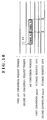
- the second A/D conversion request trigger s1 in FIG. 10 only is generated.
- the control unit 1-4 renews the second A/D conversion request trigger and instructs the switching section 1-5 to sequentially make terminals selected by the second terminal selecting section 1-3 or the terminal numbers 2 and 5 effective.
- the voltage applied to the terminal number 2 is supplied to the A/D conversion unit 1-6 and then the control unit 1-4 instructs the A/D conversion unit 1-6 to start an execution of the A/D conversion.
- the control unit 1-4 instructs the second conversion result storage register 1-8 to renew the present storage value.
- the voltage applied to the terminal 5 in place of the terminal 2 is supplied to the A/D conversion unit 1-6 through the switching section 1-5, and the control unit 1-4 instructs the A/D conversion unit 1-6 to start an execution of the A/D conversion. After the completion of the A/D conversion, the control unit 1-4 again instructs the first conversion result storage register 1-7 to renew the stored value. At this time, the first conversion result storage register 1-7 maintains a previous value without change.
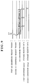
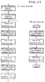
- the second A/D conversion request trigger is supplied upon execution of the A/D conversion with the first A/D conversion request trigger where the interrupt condition is fulfilled by a hardware on the process of the program execution of the flow (A) of FIG. 13 to shift the processing to the flow (B) for execution of the A/D conversion.
- the second A/D conversion request trigger s2 is supplied to the control unit 1-4 during execution of A/D conversion of the terminal 3 on the process where the terminal numbers 1, 3 and 5 are sequentially A/D converted by the first A/D conversion request trigger m2. Then, the control unit 1-4 instructs the A/D conversion unit 1-6 to interrupt the A/D conversion under execution. The control unit 1-4 instructs the switching section 1-5 to make terminal selected by the first terminal selecting section 1-2 or the terminal number 3 ineffective and to make the terminal selected by the second terminal selecting section 1-3 or the terminal number 2 effective.
- the voltage applied to the terminal number 2 is supplied to the A/D conversion unit 1-6 and the control unit 1-4 instructs the A/D conversion unit 1-6 to start an actuation of A/D conversion.
- the control unit 1-4 instructs the second conversion result storage register 1-8 to renew the present storage value by the converted value of the just completed A/D conversion.
- the A/D conversion once started by the first A/D conversion request trigger is interrupted during conversion of the terminal number 3.
- the first A/D conversion result storage register 1-7 is not renewed and the A/D conversion result of the terminal 1 remains stored.
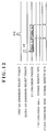
- the first A/D conversion request trigger m3 is supplied during execution of A/D conversion by the second A/D conversion request trigger s3 of FIG. 12 like the first embodiment.
- the control unit 1-4 is also provided with such function that the control unit 1-4 does never receive the first A/D conversion request trigger m3 during execution of the A/D conversion of the second A/D conversion request trigger s3.
- the first A/D conversion request trigger the A/D conversion of an analog voltage to be applied to an analog input terminal selected by the second terminal selecting section is started.
- the second A/D conversion request trigger the second A/D conversion request trigger is supplied on execution of the A/D conversion to interrupt the A/D conversion under execution so that the A/D conversion of analog voltage, which is applied to an analog input terminal selected by the second terminal selecting section, is started.
- the first A/D conversion request trigger is supplied on execution of the A/D conversion, so that at least the A/D conversion under execution is interrupted until completion of the conversion.
- the A/D conversion with the temporary interrupt processing and change of selection of analog input terminals may be carried out conveniently.
- the period from the instant when an A/D conversion value of the terminal selected by the second terminal selecting section is required to the instant when the converted value is actually obtained may considerably be reduced. Since the A/D conversion result storage register is prepared at every terminal selecting section, the stored value of the first conversion result storage register is never destructed broken by the A/D conversion with the second A/D conversion request trigger, and at any time, the last A/D conversion value of the terminal selected by the first terminal selecting section may be picked up.
- the first conversion result storage register is sometime not renewed by one time or is delayed. This is however substantially the same as the converted result is submitted to the customer's observation before completion of conversion in view point of the customer on an actual problem.
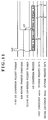
- a delay time "t" of FIG. 6 is caused under the condition of transmission to the flow (B) or the period from the instant when the A/D conversion value of the terminal selected by the second terminal selecting section is required to the instant when the second A/D conversion request trigger is generated.
- the delay time "t" is staggered in value.
- fulfillment of such transition condition to the flow (B) is determined by a hardware to carry out the transition to the flow (B) and the generation of the second A/D conversion request trigger, so that the delay time "t" from the transition against the flow (B) to the generation of second A/D conversion request trigger is negligible as shown in FIG. 11, with the minimized staggering.
Landscapes
- Engineering & Computer Science (AREA)
- Theoretical Computer Science (AREA)
- Analogue/Digital Conversion (AREA)
Applications Claiming Priority (2)
| Application Number | Priority Date | Filing Date | Title |
|---|---|---|---|
| JP3031269A JPH04271521A (ja) | 1991-02-27 | 1991-02-27 | アナログ・デジタル変換器 |
| JP31269/91 | 1991-02-27 |
Publications (2)
| Publication Number | Publication Date |
|---|---|
| EP0502428A2 true EP0502428A2 (fr) | 1992-09-09 |
| EP0502428A3 EP0502428A3 (en) | 1994-08-10 |
Family
ID=12326618
Family Applications (1)
| Application Number | Title | Priority Date | Filing Date |
|---|---|---|---|
| EP19920103405 Withdrawn EP0502428A3 (en) | 1991-02-27 | 1992-02-27 | Analog/digital converter |
Country Status (3)
| Country | Link |
|---|---|
| EP (1) | EP0502428A3 (fr) |
| JP (1) | JPH04271521A (fr) |
| KR (1) | KR920017372A (fr) |
Cited By (2)
| Publication number | Priority date | Publication date | Assignee | Title |
|---|---|---|---|---|
| WO2005011124A1 (fr) * | 2003-07-31 | 2005-02-03 | Philips Intellectual Property & Standards Gmbh | Procede et dispositif permettant une conversion analogique/numerique multicanaux |
| EP1771048A3 (fr) * | 2000-09-15 | 2007-04-11 | TridonicAtco GmbH & Co. KG | Ballast électronique avec une unité de commande numérique |
Family Cites Families (7)
| Publication number | Priority date | Publication date | Assignee | Title |
|---|---|---|---|---|
| JPS63143624A (ja) * | 1986-12-08 | 1988-06-15 | Fuji Electric Co Ltd | 多点アナログ信号入力方式 |
| JPH01112823A (ja) * | 1987-10-27 | 1989-05-01 | Fanuc Ltd | A/d変換回路 |
| JPH01147618A (ja) * | 1987-12-02 | 1989-06-09 | Matsushita Electric Ind Co Ltd | A/d変換装置 |
| JPH01258020A (ja) * | 1988-04-07 | 1989-10-16 | Toshiba Corp | データ読込み装置 |
| EP0350932B1 (fr) * | 1988-07-13 | 1996-04-10 | Nec Corporation | Processeur de données monopuce à convertisseur analogique-numérique incorporé |
| US4933676A (en) * | 1989-06-12 | 1990-06-12 | Technology 80, Inc. | Programmable multi-input A/D converter |
| JPH0330520A (ja) * | 1989-06-27 | 1991-02-08 | Sharp Corp | アナログ/デジタル変換器 |
-
1991
- 1991-02-27 JP JP3031269A patent/JPH04271521A/ja active Pending
-
1992
- 1992-02-27 EP EP19920103405 patent/EP0502428A3/en not_active Withdrawn
- 1992-02-27 KR KR1019920003074A patent/KR920017372A/ko not_active Ceased
Cited By (2)
| Publication number | Priority date | Publication date | Assignee | Title |
|---|---|---|---|---|
| EP1771048A3 (fr) * | 2000-09-15 | 2007-04-11 | TridonicAtco GmbH & Co. KG | Ballast électronique avec une unité de commande numérique |
| WO2005011124A1 (fr) * | 2003-07-31 | 2005-02-03 | Philips Intellectual Property & Standards Gmbh | Procede et dispositif permettant une conversion analogique/numerique multicanaux |
Also Published As
| Publication number | Publication date |
|---|---|
| JPH04271521A (ja) | 1992-09-28 |
| KR920017372A (ko) | 1992-09-26 |
| EP0502428A3 (en) | 1994-08-10 |
Similar Documents
| Publication | Publication Date | Title |
|---|---|---|
| EP0502428A2 (fr) | Convertisseur analogique-numérique | |
| JPH07131349A (ja) | アナログ/デジタル変換器 | |
| EP0959360B1 (fr) | Méthode de régulation de trame | |
| US6708197B1 (en) | Method of driving timer in an advanced intelligent network switching system employing the thread call structure under UNIX system | |
| US5760721A (en) | Analog-to-digital conversion device | |
| JP2956201B2 (ja) | 画像信号のタスク分割並列処理方法 | |
| US6194232B1 (en) | Multi-track wafer processing method | |
| CN120729312B (zh) | 一种共享资源的突发信号检测方法 | |
| US8564468B2 (en) | Sequence arbiter for analog-to-digital conversions | |
| JP3085371B2 (ja) | 連想記憶メモリ検索回路 | |
| SU1231486A1 (ru) | Многоканальное устройство дл программного управлени | |
| JP2025106710A (ja) | 半導体装置 | |
| JPH0877133A (ja) | A/d変換装置 | |
| JPS628814B2 (fr) | ||
| JPH0470915A (ja) | 情報処理装置の電源制御方式 | |
| JPH10173526A (ja) | 逐次比較型a/d変換回路 | |
| JPH076059A (ja) | プログラム実行状態確認方法 | |
| JP2002215593A (ja) | データ処理装置 | |
| JPH04313918A (ja) | 逐次比較型a/d変換器 | |
| JPH07506204A (ja) | 現在状態から後続状態へのプロセッサ作動状態移行制御装置 | |
| JPH04255116A (ja) | アナログ・ディジタル変換回路 | |
| KR0175399B1 (ko) | 오버샘플링 디지탈 필터에서의 데이타 제어기 | |
| JPH03223905A (ja) | シーケンスコントローラ | |
| JPH1185465A (ja) | 演算制御装置 | |
| JPH05266218A (ja) | アナログ−ディジタル変換制御装置 |
Legal Events
| Date | Code | Title | Description |
|---|---|---|---|
| PUAI | Public reference made under article 153(3) epc to a published international application that has entered the european phase |
Free format text: ORIGINAL CODE: 0009012 |
|
| AK | Designated contracting states |
Kind code of ref document: A2 Designated state(s): DE FR GB NL |
|
| 17P | Request for examination filed |
Effective date: 19920828 |
|
| PUAL | Search report despatched |
Free format text: ORIGINAL CODE: 0009013 |
|
| AK | Designated contracting states |
Kind code of ref document: A3 Designated state(s): DE FR GB NL |
|
| STAA | Information on the status of an ep patent application or granted ep patent |
Free format text: STATUS: THE APPLICATION IS DEEMED TO BE WITHDRAWN |
|
| 18D | Application deemed to be withdrawn |
Effective date: 19950901 |