EP0502436A2 - ATM-Zellenvermittlungssystem - Google Patents
ATM-Zellenvermittlungssystem Download PDFInfo
- Publication number
- EP0502436A2 EP0502436A2 EP92103448A EP92103448A EP0502436A2 EP 0502436 A2 EP0502436 A2 EP 0502436A2 EP 92103448 A EP92103448 A EP 92103448A EP 92103448 A EP92103448 A EP 92103448A EP 0502436 A2 EP0502436 A2 EP 0502436A2
- Authority
- EP
- European Patent Office
- Prior art keywords
- cell
- address
- buffer memory
- output
- read
- Prior art date
- Legal status (The legal status is an assumption and is not a legal conclusion. Google has not performed a legal analysis and makes no representation as to the accuracy of the status listed.)
- Granted
Links
Images





Classifications
-
- H—ELECTRICITY
- H04—ELECTRIC COMMUNICATION TECHNIQUE
- H04L—TRANSMISSION OF DIGITAL INFORMATION, e.g. TELEGRAPHIC COMMUNICATION
- H04L12/00—Data switching networks
- H04L12/54—Store-and-forward switching systems
- H04L12/56—Packet switching systems
- H04L12/5601—Transfer mode dependent, e.g. ATM
-
- H—ELECTRICITY
- H04—ELECTRIC COMMUNICATION TECHNIQUE
- H04J—MULTIPLEX COMMUNICATION
- H04J3/00—Time-division multiplex systems
- H04J3/24—Time-division multiplex systems in which the allocation is indicated by an address the different channels being transmitted sequentially
- H04J3/247—ATM or packet multiplexing
-
- H—ELECTRICITY
- H04—ELECTRIC COMMUNICATION TECHNIQUE
- H04L—TRANSMISSION OF DIGITAL INFORMATION, e.g. TELEGRAPHIC COMMUNICATION
- H04L12/00—Data switching networks
- H04L12/54—Store-and-forward switching systems
- H04L12/56—Packet switching systems
- H04L12/5601—Transfer mode dependent, e.g. ATM
- H04L12/5602—Bandwidth control in ATM Networks, e.g. leaky bucket
-
- H—ELECTRICITY
- H04—ELECTRIC COMMUNICATION TECHNIQUE
- H04L—TRANSMISSION OF DIGITAL INFORMATION, e.g. TELEGRAPHIC COMMUNICATION
- H04L49/00—Packet switching elements
- H04L49/10—Packet switching elements characterised by the switching fabric construction
- H04L49/104—Asynchronous transfer mode [ATM] switching fabrics
- H04L49/105—ATM switching elements
- H04L49/108—ATM switching elements using shared central buffer
-
- H—ELECTRICITY
- H04—ELECTRIC COMMUNICATION TECHNIQUE
- H04L—TRANSMISSION OF DIGITAL INFORMATION, e.g. TELEGRAPHIC COMMUNICATION
- H04L49/00—Packet switching elements
- H04L49/20—Support for services
- H04L49/201—Multicast operation; Broadcast operation
- H04L49/203—ATM switching fabrics with multicast or broadcast capabilities
-
- H—ELECTRICITY
- H04—ELECTRIC COMMUNICATION TECHNIQUE
- H04L—TRANSMISSION OF DIGITAL INFORMATION, e.g. TELEGRAPHIC COMMUNICATION
- H04L49/00—Packet switching elements
- H04L49/25—Routing or path finding in a switch fabric
- H04L49/253—Routing or path finding in a switch fabric using establishment or release of connections between ports
- H04L49/255—Control mechanisms for ATM switching fabrics
-
- H—ELECTRICITY
- H04—ELECTRIC COMMUNICATION TECHNIQUE
- H04Q—SELECTING
- H04Q11/00—Selecting arrangements for multiplex systems
- H04Q11/04—Selecting arrangements for multiplex systems for time-division multiplexing
- H04Q11/0428—Integrated services digital network, i.e. systems for transmission of different types of digitised signals, e.g. speech, data, telecentral, television signals
- H04Q11/0478—Provisions for broadband connections
-
- H—ELECTRICITY
- H04—ELECTRIC COMMUNICATION TECHNIQUE
- H04L—TRANSMISSION OF DIGITAL INFORMATION, e.g. TELEGRAPHIC COMMUNICATION
- H04L12/00—Data switching networks
- H04L12/54—Store-and-forward switching systems
- H04L12/56—Packet switching systems
- H04L12/5601—Transfer mode dependent, e.g. ATM
- H04L2012/5638—Services, e.g. multimedia, GOS, QOS
-
- H—ELECTRICITY
- H04—ELECTRIC COMMUNICATION TECHNIQUE
- H04L—TRANSMISSION OF DIGITAL INFORMATION, e.g. TELEGRAPHIC COMMUNICATION
- H04L12/00—Data switching networks
- H04L12/54—Store-and-forward switching systems
- H04L12/56—Packet switching systems
- H04L12/5601—Transfer mode dependent, e.g. ATM
- H04L2012/5672—Multiplexing, e.g. coding, scrambling
Definitions
- the present invention relates to a switching system, or more in particular to an ATM (Asynchronous Transfer Mode) switching system used with the speech path equipment of a wide-bandwidth ISDN exchange and, especially, an ATM switching system suitable for accommodating a plurality of types of input-output links having different transmission rates.
- ATM Asynchronous Transfer Mode
- a "TDM Switching System” proposed by JP-A-59-135994 is known, for example, as an ATM switching system applied to the wide-bandwidth ISDN exchange.
- This switching system comprises a multiplexer for multiplexing a fixed-length packet (hereinafter referred to as "the cell") inputted from each input line, a buffer memory for inputting a multiplexed cell, a demultiplexer for periodically separating the cells outputted from the buffer memory among output lines, and a buffer memory control circuit for controlling the buffer memory for each output line.
- the buffer memory control circuit which includes FIFO (First In First Out) memories corresponding to the output lines, inputs a write address for the buffer memory into a FIFO memory corresponding to the cell output destination judged from the header information of a cell when the cell is written into the buffer memory. Also, the cell output from the buffer memory corresponding to each output line is produced at predetermined time intervals so that a read address is outputted to the buffer memory from the FIFO memory corresponding to each output line in timing with the cell output.
- FIFO First In First Out
- the reading of a cell from the buffer memory is controlled to a predetermined timing for each output line.
- a packet switching system capable of accommodating a plurality of types of input/output links having different transmission rates is proposed in JP-A-63-64439, for example, as a system for controlling the write and read operations of a packet with a buffer memory using a control memory.
- a plurality of input and output ports of a switch unit are matched one to one with input and output lines respectively, and packets are inputted and outputted to these input/output ports at a rate equal to the data transmission rate of the input/output lines connected thereto.
- the number of an input line providing an objective of the packet write process or an output line providing an objective of the packet read process within a predetermined regular time interval and the R/W designated data are stored in the control memory according to the processing sequence in such a manner as to generate the R/W process at a frequency corresponding to the data transmission rate of each line.
- the contents (the line numbers and the R/W designated data) of the control memory are sequentially read with the counter output value as an address and packets are written into or read from the buffer memory for the input/output lines designated by the line number thus read out.
- the switching system described above is such that the buffer memory access is sequentially controlled in such a manner that packets are processed at the switching unit input port (or switch unit output port) connected to a high-speed input line (or output line) at a higher frequency than at the switch unit input port (or switch unit output port) connected to a low-speed input line (or output line).
- An object of the present invention is to provide an ATM switching system capable of a cell switching operation in accordance with the cell transmission rate of an output line to be accommodated.
- Another object of the present invention is to provide an ATM switching system which can accommodate output lines of a plurality of different transmission rates including, say, 600 Mbps, 150 Mbps and 50 Mbps with a comparative freedom.
- an ATM switching system comprises a switch unit including a plurality of switch unit input ports and switch unit output ports having a first transmission rate respectively, a plurality of input lines (input links), a plurality of output lines (output links), and at least one conversion means inserted between at least one of the output lines and at least one of the switch unit output ports and having a second transmission rate different from the first transmission rate for converting a cell train of the first transmission rate into a cell train of the second transmission rate, wherein: the switch unit includes multipexing means for multiplexing and outputting a plurality of cell trains inputted from the switch unit input ports as a cell train, a shared buffer memory for temporarily storing the cell trains outputted sequentially from the multiplexer means, demultiplexing means for distributing in circulation the cells read from the shared buffer memory among the switch unit output ports, and a buffer memory control circuit for controlling the write and read operations of cells from the shared buffer memory; and the buffer memory control circuit includes control table
- At least one conversion means for converting an input cell train into a cell train of the first transmission rate may be connected between at least one of the input lines having a transmission rate different from the first transmission rate and at least one of the switch unit input ports.
- the internal links connected to the output ports of the switch unit are set to the same transmission rate and that the output cells from the internal output links are bundled together by a multiplexer (a kind of conversion means), for example, the cell transmission rate at the output lines connected to the multiplexer can be increased.
- the output cell from an internal output link may be distributed among a plurality of output lines by a demultiplexer (a kind of conversion means) thereby to reduce the cell transmission rate at each output line.
- a quadruple multiplexer is installed for an internal output link having a transmission rate of 150 Mbps, for example, it is possible to realize an output line having a transmission rate of 600 Mbps.
- an output line having a transmission rate of 50 Mbps is realized by providing a demultiplexer of three divisions.
- the technical task is how to control the buffer by a buffer memory control circuit.
- the above-mentioned multiplexer or demultiplexer is installed at the output port side of the ATM switching unit and the cell queue chain access is controlled in accordance with the output line (output link) connected to the multiplexer or demultiplexer respectively.
- the above-mentioned control table means has stored therein an output line identifier corresponding to the timing of cell output to the switch unit output ports.
- a switch unit output port is selected and a table addressed sequentially in circulation, so that in timing with the cell output to each output port, the output line identifier for specifying a queue chain to which the cell to be outputted to the particular output port belongs is read from a control table thereby to read a cell from the queue chain.
- the output ports of the switch unit are set to the same cell transmission rate and a new speed change means (multiplexer or demultiplexer) is added between the output port and the output link or is replaced with other appropriate means in accordance with the transmission rate required by the output link thereby to enable comparatively free selection of cell transmission rate on each output line.
- a new speed change means multiplexer or demultiplexer
- the contents of the control table are simply modified by external microcomputer control or the like means.
- the transmission rate of the output lines can be easily changed.
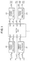
- Fig. 1 is a diagram showing a configuration of a switching system having multiple-speed input-output ports according to an embodiment of the present invention.
- Fig. 2 is a diagram showing a configuration of a switching system comprising a bandwidth control table according to an embodiment of the present invention.
- Fig. 3 is a diagram for explaining the operation of a 150 Mbps/600 Mbps multiplexer shown in Fig. 2.
- Fig. 4 is a diagram for explaining the operation of switches between a shared buffer memory and an output port.
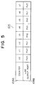
- Fig. 5 is a diagram showing the relationship between a counter value and an output port stored in a bandwidth control table.
- Fig. 6 is a diagram showing an example of configuration of a switch expanded according to the present invention.
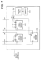
- Fig. 7 is a diagram showing an example of configuration of a buffer memory control circuit for realizing the multicast function according to the present invention.
- Fig. 8 is a diagram showing the relationship between a counter value and various values stored in a bandwidth control table having the multicast function.
- Fig. 9 is a diagram for explaining the operation timing between a shared buffer memory and an output port in a switch having the multicast function.
- Fig. 10 is a diagram showing an example of configuration of a buffer memory control circuit for realizing the QOS (Quality of Service) class function.
- QOS Quality of Service
- Fig. 11 is a diagram showing a buffer memory control circuit having the QOS function according to another embodiment.
- Fig. 1 shows an example of configuration of an ATM switch comprising a pair of line input/output ports (PiO, PoO) connected with a line having the transmission rate of 300 Mbps, a pair of line input/output ports (Pi1, Po1) connected with a line of 150 Mbps and two pairs of line input/output ports (Pi2/Po2, Pi3/Po3) connected with a line of 75 Mbps.
- PiO, PoO line input/output ports
- reference numeral 1 designates a switch unit including switch unit input ports Si0 to Si3 connected respectively with internal input links (L14, L15, L11, L16) having a transmission rate of 150 Mbps and switch unit output ports So0 to So3 connected respectively with internal output links (L50 to L53) of 150 Mbps.
- Numeral 20 designates a 300 Mbps/150 Mbps demultiplexer connected between the internal input ports Si0, Si1 and the line input port Pi0, and numeral 21 a 75 Mbps/150 Mbps multiplexer inserted between the internal input port Si3 and the line input ports Pi2, Pi3.
- Numeral 22 designates a 150 Mbps/300 Mbps multiplexer connected between the internal output ports So0, So1 and the line output port Po0, and numeral 23 a 150 Mbps/75 Mbps demultiplexer connected between the internal output port So3 and the line output ports Po2, Po3.
- a cell train inputted from the line input port Pi0 through the internal input link L10 at a transmission rate of 300 Mbps is distributed alternately between the internal input links L14 and L15 at the demultiplexer of 300 Mbps/150 Mbps, and the resulting two cell trains having a transmission rate of 150 Mbps are inputted to the switch unit 1.
- the cell train of 150 Mbps inputted from the line input port Pi1 is inputted to the switch unit 1 directly without being converted in speed.
- the two cell trains of 75 Mbps inputted through the internal input links L12, L13 from the line input ports Pi2, Pi3, on the other hand, are multiplexed alternately on the internal input link L16 at the multiplexer 21 of 75 Mbps/150 Mbps, and the resulting single cell train having a transmission rate of 150 Mbps is inputted to the switch unit 1.
- each cell train outputted to the internal output links L50, L51 is multiplexed alternately at the multiplexer of 150 Mbps/300 Mbps, and is outputted as a cell train having a transmission rate of 300 Mbps through the internal output link L54 to the line output port Po0.
- Each cell outputted to the internal output link L52 is outputted from the line output port Po1 at the same speed of 150 Mbps.
- Each cell outputted to the internal output link L53 is distributed alterantely between the internal output links L55 and L56 at the demultiplexer 22 of 150 Mbps/75 Mbps, and is outputted to the line output ports Po2, Po3 respectively at a rate of 75 Mbps.
- the internal links of the line input/output ports Pi0 to Pi3 and Po0 to Po3 have installed therein line interfaces for rewriting the cell header, although not shown in Fig. 1 for the sake of simplicity.
- the functions of the demultiplexers 20, 23 and the multiplexers 21, 22 may be integrated with the line interface.
- Fig. 2 shows an example of configuration of the switch unit 1.
- the switch unit 1 includes a multiplexer 12 of 150 Mbps/600 Mbps connected with the switch unit input ports Si0 to Si3 (or the internal input links L11, L14 to L16), a shared buffer memory 11 for temporarily storing the cells inputted sequentially through the port-designating information extraction circuit 14 and the line L2 from the multiplexer 12, a demultiplexer 13 of 600 Mbps/150 Mbps connected to the switch unit output ports So0 to So3 (or the internal output links L50 to L53), and a buffer memory control circuit 10.
- the buffer memory control circuit 10 includes a write address memory 101, a read address memory 102, an idle address buffer 103, a control table 104 and a counter 105.
- the cells inputted to the switch unit 1 at a transmission rate of 150 Mbps through the internal input links L14, L15, L11 and L16 are multiplexed sequentially at the multiplexer 12 of 150 Mbps/600 Mbps and are inputted to the shared buffer memory 11 at a rate of 600 Mbps.
- the cell of 600 Mbps outputted from the shared buffer memory 11 by the buffer memory control circuit 10, on the other hand, is demultiplexed sequentially among the switch unit output ports So0 to So3 at the 600 Mbps/150 Mbps demultiplexer 13 and is distributively outputted to the internal output links L50 to L53 of 150 Mbps.
- the buffer memory control circuit 10 for controlling the write and read operations of the shared buffer memory 11 receives the line output port-designating information from the extraction circuit 14 through the line L30 during the time of writing cells into the shared buffer memory 11, and makes access to the write address memory 101 with the same information as an address.
- the address which is thus read from the write address memory 101 is applied to the write address WA of the shared buffer memory 11 through the line L32.
- an idle address is outputted to the line L31 from an idle address buffer 103 storing idle addresses not in use at the shared buffer memory 11, and is written as "the next address" in the shared buffer memory 11 and the write address memory 101.
- This next address (idle address) is written in the memory position of the same address as the one wherefrom the write address has been read at the write address memory 101. Also, in the shared buffer memory 11, the next address mentioned above is written in a memory region specified by the same address as the input cell. This next address is indicative of the cell address of the shared buffer memory to be written the next time which is outputted to the same line output port as the input cell, whereby a queue chain for each output line is formed.
- the line identifier is outputted from the control table 104 in accordance with the switch unit output port selected by the demultiplexer 13, and the line identifier is used to designate a queue chain to be accessed for reading in the buffer memory 11. More specifically, the line identifier outputted from the control table 104 is applied as a read address RA and a write address WA to the read address memory 102, and a cell address in a queue chain is outputted to the line L33. On the bais of this address, the next address is read out of the shared buffer memory 11 together with a cell in the queue chain.
- the next address is stored in an address position corresponding to the line identifier in the read address memory 102 so that the cell to be read the next time from the queue chain may be specified.
- an address chain (linked list) due to the next address is configured for each line output port.
- the reading operation of cells from the shared buffer memory 11 is controlled in a manner that will be mentioned.
- the counter 105 counts up each time of reading a cell from the shared buffer memory 11.
- a count value changing in circulation is outputted from the counter 105 and is applied as an address to the control table 104.
- the control table 104 in turn outputs a line identifier (line output port-specifying information) stored at the storage position in accordance with the count value.
- This line identifier is applied to the read address memory 102 as a read/write address.
- the above-mentioned address causes a read address to be read out on the line L33 for reading a cell from a specified queue chain corresponding to the line output port in the shared buffer memory 11 from the read address memory 102.
- the shared buffer memory 11 By accessing the shared buffer memory 11 using this read address, a cell addressed to a line output port specified by the line identifier is read. In the process, the read address outputted from the shared buffer memory 11 becomes idle upon completion of the cell read operation, and therefore is stored in the idle address buffer 102 through the line L33. Also, the next address read simultaneously with the cell from the shared buffer memory 11 is written into the read address memory 102 in order to read the next cell from the queue chain. Each time of the above-mentioned reading operation, the queue chain is compressed by a cell. The detailed operation of the counter 105 and the bandwidth control table 104 will be described later.
- Fig. 3 shows the operation of the multiplexer 12 of 150 Mbps/600 Mbps connected with the switch unit input ports Si0 to Si3.
- the cells on the switch unit input ports Si0 to Si3 (internal input links L14, L15, L11, L16) have a transmission rate of 150 Mbps and are applied to the multiplexer 12 at slightly different timings from each other.
- the multiplexer 12 multiplexes the input cells from the input port lines sequentially and outputs them to the line L2 at a transmission rate of 600 Mbps.
- a similar operation is performed by the 75 Mbps/150 Mbps multiplexer 21 connected to the line input ports Pi2, Pi3 and the 150 Mbps/300 Mbps multiplexer 22 connected to the line output port Po0.
- the demultiplexer 13 of 600 Mbps/150 Mbps connected to the switch unit output ports So0 to So3 demultiplexes the input cells in a manner reverse in cell input/output timing of the 150 Mbps/600 Mbps multiplexer 12 shown in Fig. 3.
- the 300 Mbps/150 Mbps demultiplexer connected to the line input port Pi0 and the 150 Mbps/75 Mbps demultiplexer 23 connected to the line output ports Po2, Po3 also operate the same way as the 600 Mbps/150 Mbps multiplexer 13.
- the sequence of the cells is maintained in the internal links L10, L2 and L4, L54 respectively.
- Fig. 4 shows the correlation between the read cells c0 to c7 from the shared buffer memory 11 to the line output ports (Po0, Po1, Po2, Po3).
- the cells c0, c1, c3,Across, c7 and so on, read out in that order on the line L4 are demultiplexed into four cell trains at the 600 Mbps/150 Mbps demultiplexer 13.
- the cells c0, c4 and so on are transferred in that order on the internal output link L50, c1, c5 and so on, in that order on the internal output link L51, c2, c6 and so on, in that order on the internal output link L52, and c3, c7 and so on, in that order on the internal output link L53.
- those on the links L50 and L51 are multiplexed by the 150 Mbps/300 Mbps multiplexer 22 and are outputted to the internal output link L54 as c0, c1, c4, c5 and so on, in that order.
- the sequence of cells is maintained in the internal output links L4 and L54.
- the cells outputted to the link 53 are demultiplexed further into two cell trains by the 150 Mbps/75 Mbps demultiplexer 23, so that the cells c3 and so on, are outputed on the internal output link L55 and the cells c7 and so on, on the internal output link L56, respectively, at a transmission rate of 75 Mbps.
- the demultiplexer 13 is adapted to sequentially distribute the cells read from the shared buffer memory 11 among the internal output links L50 to L53. Therefore, the line output ports to which cells are sent are determined by the timing at which cells are outputted from the shared buffer memory 11.
- line identifiers Po0 to Po3 are outputted as shown in Fig. 5 from the control table 104 in accordance with the count value of the counter 105 (table address).
- the count values (table addresses) in the column 104A are shown with cell codes (output timings) shown in Fig. 4.
- the line identifiers stored in the column 104B of the control table 104 are addressed in circulation by the count values of the counter 105, so that the output line identifiers Po0, Po0 corresponding to the count values c0, c1 and so on, are outputted at the output timing of c8, c9 and so on, following the cell c7.
- control table 104 can be rewritten freely by the control of the processor of a call control unit or another microcomputer not shown, for example.
- the speed of each input/output link connected to the switching system can be freely changed by rewriting the values of the output line identifiers in the control table 104 corresponding to the speed change means.
- each of the links L10 and L54 can be demultiplexed into two input/output links of 75 Mbps respectively.
- the virtual path or channel should be distributed at storage positiosns addressed by the count values c3, c7 in the control table 104.
- the 150 Mbps link can be demultiplexed into bands other than mentioned above. It is, however, necessary to change the period of the counter 105.
- Fig. 6 shows an example of switch unit configuration including a plurality of unit switches with 4x4 input/output ports which is enlarged to have 8x8 input/output ports.
- the unit switches 1-5, 1-6, 1-7 and 1-8 in the rear stage are operated as the ones substantially having 4x2 input/output links with two of the four output links left unused.
- the four input ports of the first unit switch 1-1 in the front stage and the four input ports of the third unit switch 1-3 are commonly connected to a 150 Mbps (first to fourth) internal input links.
- the unit switch 1-1 is adapted to apply, of all the input cells from the internal input links, only the cells destined for the unit switchs 1-5 and 1-6 to the shared buffer memory 11, and in accordance with the port identification information of each cell, distributes the cells among the unit switches in the rear stage.
- the unit switch 1-3 causes only the input cells destined for the unit switches 1-7 and 1-8 in the rear stage to the shared buffer memory, and distributes these cells among the unit switches in the rear stage.
- the unit switches 1-2 and 1-4 in the front stage are commonly connected to the four (fifth to eighth) input links.
- the unit switch 1-2 receives only the input cells destined for the unit switches 1-5 and 1-6 in the rear stage, and the switch 1-4 only those input cells destined for the unit switches 1-7 and 1-8 in the rear stage, respectively, thereby performing the switching operation in accordance with the port identification information of the cells.
- Each of the unit switches 1-1, 1-2, 1-3 and 1-4 in the front stage has four 150 Mbps output ports. Since every unit switch operates to distribute cells among two unit switches in the rear stage, however, the switches in the front stage is theoretically operated as having two 300 Mbps output ports as a whole. In this case, a control table for the unit switches 1-1, 1-2, 1-3 and 1-4 in the front stage is designed on the assumption that there exists a link of 300 Mbps between the switch groups in the front and rear stages, thereby making it possible to transmit cells with a throughput of 300 Mbps within the switch unit.
- a second embodiment of the present invention will be explained below with reference to an example of a switching system having the multicast function utilizing a control table as shown in Figs. 7 to 9.
- Fig. 7 is a diagram showing an example of configuration of a buffer memory control circuit 10 for realizing the multicast function.
- the write address memory 101 and the read address memory 102 are controlled for each virtual path (VP).
- the control table 104' has the function of outputting an END signal for controlling the repetition of the same read address in addition to the virtual path VP for specifying the queue chain to be accessed.
- the END signal In reading a multicast cell, the END signal is held at "0" level until the sampe multicast cell is completely read out a required number of times, whereby the addresses in the idle address buffer 103 and the read address memory 102 are updated.
- the END signal is raised to '1' level, whereby the read address memory 102 and the idle address buffer 103 update the address.
- Fig. 8 shows an example of the data stored in the control table 104' for muticasting as mentioned above, and Fig. 9 an operation timing of the cell output from the switch unit 11 in the control table.
- the line identifiers 104B are shown by the virtual path number. Of all these virtual path numbers, VP0, VP1, VP2 and VP3 are for non-multicast cells, and VP4 and VP5 for multicast cells.
- the multicast cells stored in a queue chain corresponding to VP4 are outputted from the buffer memory 11 when the count value (address) 104A is c0, c1, c3.
- the END signal 104C is '0', and therefore the next address in the read address memory 102 is not updated.
- an address designating the same cell in the queue chain corresponding to VP4 is outputted repetitively from the read address memory 102, so that the same cell is outputted repetitively from the shared buffer memory 11.
- the END signal is turned to '1', and a new next address is stored in the read address memory 102. Therefore, a new cell is multicast at the time of reading class of VP4 in the next cycle.
- the operation of reading the multicast contained in the queue chain of VP5 for which the count value is read out at the timing of c9, c10 is also performed in the same manner as mentioned above.
- the cells read out at other timings are non-multicast cells. With regard to these cells, the END signal is always kept at '1' to update the address memory to enable a new cell to be read out in the next cycles each time a cell is read out.
- Fig. 9 is a diagram showing the cell output operation from a switch unit with the control table 104' shown in Fig. 8.
- the cells stored in the queue chain of VP4 are multicast to the lines L50, L51, L53, and the cells of VP5 to the links L51, L52.
- the cells stored in the queue chain of VP0 are outputted to the link L50, the cells in the queue chain of VP1 to the link L51, the cells in the queue chain of VP2 to the link L52, and the cells in the queue chain of VP3 to the link L53.
- Fig. 10 shows an example of configuration of a buffer memory control circuit 10 having the QOS class control function.
- an extraction circuit 14 shown in Fig. 2 is adapted to extract the class designating information (CLS) and VP from the input cell header and apply them to the buffer memory control circuit 10 through the line L30.
- CLS class designating information
- the write addresses WA1, WA1' are read out of the write address memories 101, 101' respectively.
- One of these write addresses WA1, WA1' is selected in accordance with the class (CLS) at a selector SEL1 and is applied through the line L32 to the shared buffer memory 11.
- CLS class
- one of the write address memories 101, 101' selected in accordance with the class CLS is set to a writable state (WEN to '1') by an output signal of a decoder DEC1, and a new address value is written on the line L30.
- the read addresses RA1, RA1' are outputted from the two read address memories 102, 102' with the VP outputted from the control table 104'' as an address.
- One of the addresses RA1 and RA1' is selected in accordance with the signal CLS' produced from the QOS control circuit 106 at the selector SEL2, and is applied through the line L33 to the shared buffer memory 11.
- the address memory 102 or 102' selected in accordance with the signal CLS' is set to a writable state (WEN in '1' state) by the output signal from the decoder DEC2, thereby storing a new next address value inputted through the line L34.
- the QOS class control circuit 106 outputs the signal CLS' in accordance with the CLS'' outputted from the control table 104''.
- a different class is selected, however, when there is no cells to be read in the class designated by the output of the control table.
- a counter is installed for each VP or class, for instance, to count the number of cells contained presently in the shared buffer memory 11. This method, however, is liable to increase the hardware quantity.
- Another method of determining the presence or absence of cells consists in comparing the values of the write address memory 101 (101') and the read address memory 102 (102') with each other in accordance with each VP or class, for instance.
- the cell absence is determined if the two addresses concide with each other, and the presence is judged if the two addresses fail to coincide with each other.
- This method saves the hardware quantity, but requires an appropriate timing in making comparison of addresses with a read address memory in a write address memory, and therefore the setting of the operation timing is stricter.
- a method for solving this problem lies, as shown in Fig. 11, in installing write address memories 107, 107' for determining the cell presence or absence in the buffer memory control circuit 10.
- the output addresses of the write address memories 107, 107' for determining the cell presence or absence are applied to comparators 108, 108' together with the output addresses of the read address memories 102, 102', and the results of comparison are applied to the QOS class control circuit 106 as a signal representing the cell presence or absence.
- an ATM switch unit comprising a plurality of output ports having the same transmission rate, in which a buffer memory control circuit includes a control table, and a cell queue chain to be read by the control table is designated in accordance with the timing of cell output to each switch unit output port in circulation.
- the interposition of a plurality of switch unit output ports having a plurality of lines and a single line port make it possible to increase the transmission rate of the output lines, while the transmission rate of the output line can be reduced by inserting a demultiplexer between a single switch unit output port and a plurality of line ports, with the result that a plurality of types of output lines having different transmission rates can be easily accommodated in a switching system.
- An ATM switching system having output links of 150 Mbps in transmission rate, for instance, is capable of housing output lines of 600 Mbps if equipped with a quadruple multiplexer.
- information for designating whether the same cell is to be read at the next reading operation may be set in a control table in addition to a line identifier for designating a queue chain for reading cells thereby to realize the multicast function controlled in band.
- a buffer memory control circuit in which a write address memory and a read address memory are disposed in a relation corresponding to the QOS class of cells, so that a QOS class is designated by a control table, thereby realizing the communications with a band assured for each QOS class.
Landscapes
- Engineering & Computer Science (AREA)
- Computer Networks & Wireless Communication (AREA)
- Signal Processing (AREA)
- Computer Hardware Design (AREA)
- Data Exchanges In Wide-Area Networks (AREA)
Applications Claiming Priority (2)
| Application Number | Priority Date | Filing Date | Title |
|---|---|---|---|
| JP3838891A JP2947956B2 (ja) | 1991-03-05 | 1991-03-05 | スイッチングシステム |
| JP38388/91 | 1991-03-05 |
Publications (3)
| Publication Number | Publication Date |
|---|---|
| EP0502436A2 true EP0502436A2 (de) | 1992-09-09 |
| EP0502436A3 EP0502436A3 (en) | 1992-10-14 |
| EP0502436B1 EP0502436B1 (de) | 1997-05-02 |
Family
ID=12523901
Family Applications (1)
| Application Number | Title | Priority Date | Filing Date |
|---|---|---|---|
| EP92103448A Expired - Lifetime EP0502436B1 (de) | 1991-03-05 | 1992-02-28 | ATM-Zellenvermittlungssystem |
Country Status (3)
| Country | Link |
|---|---|
| EP (1) | EP0502436B1 (de) |
| JP (1) | JP2947956B2 (de) |
| DE (1) | DE69219390T2 (de) |
Cited By (10)
| Publication number | Priority date | Publication date | Assignee | Title |
|---|---|---|---|---|
| FR2700865A1 (fr) * | 1993-01-27 | 1994-07-29 | Alcatel Nv | Dispositif de gestion de mémoire tampon de cellules. |
| EP0748087A1 (de) * | 1995-06-09 | 1996-12-11 | International Business Machines Corporation | Zugriffsteuerungssystem eines gemeinsamen Pufferspeichers |
| EP0707397A3 (de) * | 1994-05-24 | 1997-07-16 | Nec Corp | Koppelfeld mit gemeinsame Pufferspeichern für ein ATM-Vermittlungssystem und zugehöriges Verfahren zum Steuern der Rundsendung |
| EP0851635A3 (de) * | 1996-12-25 | 2001-09-05 | Hitachi, Ltd. | IP Vermittlungsstelle, Schnittstellenschaltung und ATM Vermittlungsstelle zur Verwendung für die IP Vermittlungsstelle, sowie ein IP Vermittlungsnetzsystem |
| EP0685949A3 (de) * | 1994-06-03 | 2002-07-10 | Philips Patentverwaltung GmbH | Paketübermittlungssystem |
| SG93800A1 (en) * | 1995-08-31 | 2003-01-21 | Sun Microsystems Inc | A scalable architecture for asynchonous transfer mode segmentation and reassembly |
| US6512745B1 (en) | 1996-03-08 | 2003-01-28 | Hitachi, Ltd. | Packet switching network, packet switching equipment, and network management equipment |
| EP1107517A3 (de) * | 1999-12-09 | 2004-04-21 | Nec Corporation | System und Verfahren zur ATM-Vermittlung von mehrfachen Übertragunsraten |
| US7403536B2 (en) * | 2002-12-19 | 2008-07-22 | International Business Machines Corporation | Method and system for resequencing data packets switched through a parallel packet switch |
| US7752375B2 (en) * | 2003-08-12 | 2010-07-06 | Hitachi, Ltd. | Input output control apparatus with a plurality of ports and single protocol processing circuit |
Families Citing this family (7)
| Publication number | Priority date | Publication date | Assignee | Title |
|---|---|---|---|---|
| KR960027803A (ko) * | 1994-12-13 | 1996-07-22 | 양승택 | 출력버퍼형 비동기 전송방식(atm) 스위치 |
| JP3643637B2 (ja) * | 1996-03-08 | 2005-04-27 | 株式会社日立コミュニケーションテクノロジー | セル出力制御回路および制御方法 |
| JP3473262B2 (ja) | 1996-04-05 | 2003-12-02 | 株式会社日立製作所 | パケット通信装置 |
| US6870854B1 (en) | 1996-06-21 | 2005-03-22 | Hitachi, Ltd. | Packet switching device and cell transfer method |
| US6046999A (en) | 1996-09-03 | 2000-04-04 | Hitachi, Ltd. | Router apparatus using ATM switch |
| JP3563257B2 (ja) | 1998-02-20 | 2004-09-08 | Necエレクトロニクス株式会社 | Atmスイッチ回路 |
| JPH11331196A (ja) | 1998-05-19 | 1999-11-30 | Nec Corp | マルチサービスクラス定義型atm交換機 |
Family Cites Families (5)
| Publication number | Priority date | Publication date | Assignee | Title |
|---|---|---|---|---|
| US4577308A (en) * | 1984-04-06 | 1986-03-18 | At&T Bell Laboratories | Multiplexed interconnection of packet switching node packages |
| DE3513083A1 (de) * | 1985-04-12 | 1986-10-23 | Standard Elektrik Lorenz Ag, 7000 Stuttgart | Breitbandiges dienstintegriertes nachrichtenuebertragungssystem |
| US4910731A (en) * | 1987-07-15 | 1990-03-20 | Hitachi, Ltd. | Switching system and method of construction thereof |
| JP2667868B2 (ja) * | 1988-04-06 | 1997-10-27 | 株式会社日立製作所 | セル・スイッチング・システム |
| DE68924191T2 (de) * | 1988-04-21 | 1996-05-09 | Nippon Electric Co | Für integrierte Schaltungsausführung geeignete Paketvermittlung. |
-
1991
- 1991-03-05 JP JP3838891A patent/JP2947956B2/ja not_active Expired - Fee Related
-
1992
- 1992-02-28 DE DE69219390T patent/DE69219390T2/de not_active Expired - Fee Related
- 1992-02-28 EP EP92103448A patent/EP0502436B1/de not_active Expired - Lifetime
Cited By (15)
| Publication number | Priority date | Publication date | Assignee | Title |
|---|---|---|---|---|
| EP0609128A1 (de) * | 1993-01-27 | 1994-08-03 | Alcatel N.V. | Verwaltungsvorrichtung von Zellenpufferspeicher |
| FR2700865A1 (fr) * | 1993-01-27 | 1994-07-29 | Alcatel Nv | Dispositif de gestion de mémoire tampon de cellules. |
| EP0707397A3 (de) * | 1994-05-24 | 1997-07-16 | Nec Corp | Koppelfeld mit gemeinsame Pufferspeichern für ein ATM-Vermittlungssystem und zugehöriges Verfahren zum Steuern der Rundsendung |
| EP0685949A3 (de) * | 1994-06-03 | 2002-07-10 | Philips Patentverwaltung GmbH | Paketübermittlungssystem |
| EP0748087A1 (de) * | 1995-06-09 | 1996-12-11 | International Business Machines Corporation | Zugriffsteuerungssystem eines gemeinsamen Pufferspeichers |
| SG93800A1 (en) * | 1995-08-31 | 2003-01-21 | Sun Microsystems Inc | A scalable architecture for asynchonous transfer mode segmentation and reassembly |
| US6512745B1 (en) | 1996-03-08 | 2003-01-28 | Hitachi, Ltd. | Packet switching network, packet switching equipment, and network management equipment |
| US7046630B2 (en) | 1996-03-08 | 2006-05-16 | Hitachi, Ltd. | Packet switching network, packet switching equipment and network management equipment |
| EP0851635A3 (de) * | 1996-12-25 | 2001-09-05 | Hitachi, Ltd. | IP Vermittlungsstelle, Schnittstellenschaltung und ATM Vermittlungsstelle zur Verwendung für die IP Vermittlungsstelle, sowie ein IP Vermittlungsnetzsystem |
| US6526045B2 (en) | 1996-12-25 | 2003-02-25 | Hitachi, Ltd. | IP switch, interface circuit and ATM switch used for IP switch, and IP switch network system |
| US6993029B2 (en) | 1996-12-25 | 2006-01-31 | Hitachi, Ltd. | IP switch, interface circuit and ATM switch used for IP switch, and IP switch network system |
| EP1107517A3 (de) * | 1999-12-09 | 2004-04-21 | Nec Corporation | System und Verfahren zur ATM-Vermittlung von mehrfachen Übertragunsraten |
| US7403536B2 (en) * | 2002-12-19 | 2008-07-22 | International Business Machines Corporation | Method and system for resequencing data packets switched through a parallel packet switch |
| US7752375B2 (en) * | 2003-08-12 | 2010-07-06 | Hitachi, Ltd. | Input output control apparatus with a plurality of ports and single protocol processing circuit |
| US8090893B2 (en) | 2003-08-12 | 2012-01-03 | Hitachi, Ltd. | Input output control apparatus with a plurality of ports and single protocol processing circuit |
Also Published As
| Publication number | Publication date |
|---|---|
| DE69219390D1 (de) | 1997-06-05 |
| EP0502436B1 (de) | 1997-05-02 |
| JPH04276943A (ja) | 1992-10-02 |
| DE69219390T2 (de) | 1997-11-20 |
| JP2947956B2 (ja) | 1999-09-13 |
| EP0502436A3 (en) | 1992-10-14 |
Similar Documents
| Publication | Publication Date | Title |
|---|---|---|
| US5799014A (en) | ATM cell switching system | |
| EP0502436B1 (de) | ATM-Zellenvermittlungssystem | |
| AU637250B2 (en) | Traffic shaping method and circuit | |
| US5099475A (en) | Switching system | |
| US6611527B1 (en) | Packet switching apparatus with a common buffer | |
| US4893304A (en) | Broadband packet switch with combined queuing | |
| US5425022A (en) | Data switching nodes | |
| US4849968A (en) | Buffer management system | |
| JPH07283825A (ja) | Atmスイッチ装置の回線接続装置のための回路装置 | |
| WO1988004870A1 (en) | Enhanced efficiency batcher-banyan packet switch | |
| US6731628B1 (en) | Circuit-switched network | |
| US20010028652A1 (en) | ATM cell switching system | |
| USRE36751E (en) | ATM switching system connectable to I/O links having different transmission rates | |
| US6330240B1 (en) | ATM cell switching system | |
| US6496513B1 (en) | Traffic priority control system for a concentration-type ATM switch | |
| EP0477242B1 (de) | Datenvermittlungsknoten | |
| JPH09116545A (ja) | Atmセル多重化装置 | |
| JP3266155B2 (ja) | スイッチングシステム | |
| JP3114721B2 (ja) | スイッチングシステム | |
| JP2001119408A (ja) | 出力バッファ型atmスイッチ | |
| KR970002817B1 (ko) | 에이티엠(atm)망에서 가상경로에 의한 링크공유 제어장치 | |
| JP2700041B2 (ja) | セル交換装置 | |
| JP2726108B2 (ja) | セル交換装置 |
Legal Events
| Date | Code | Title | Description |
|---|---|---|---|
| PUAI | Public reference made under article 153(3) epc to a published international application that has entered the european phase |
Free format text: ORIGINAL CODE: 0009012 |
|
| PUAL | Search report despatched |
Free format text: ORIGINAL CODE: 0009013 |
|
| AK | Designated contracting states |
Kind code of ref document: A2 Designated state(s): DE FR GB |
|
| AK | Designated contracting states |
Kind code of ref document: A3 Designated state(s): DE FR GB |
|
| 17P | Request for examination filed |
Effective date: 19921110 |
|
| 17Q | First examination report despatched |
Effective date: 19950307 |
|
| GRAG | Despatch of communication of intention to grant |
Free format text: ORIGINAL CODE: EPIDOS AGRA |
|
| GRAH | Despatch of communication of intention to grant a patent |
Free format text: ORIGINAL CODE: EPIDOS IGRA |
|
| RIN1 | Information on inventor provided before grant (corrected) |
Inventor name: GOHARA, SHINOBU Inventor name: AOKI, KAORU Inventor name: ITO, YUTAKA Inventor name: AIKI, KIYOSHI Inventor name: YANAGI, JUNICHIROU Inventor name: KOZAKI, TAKAHIKO |
|
| GRAH | Despatch of communication of intention to grant a patent |
Free format text: ORIGINAL CODE: EPIDOS IGRA |
|
| GRAA | (expected) grant |
Free format text: ORIGINAL CODE: 0009210 |
|
| AK | Designated contracting states |
Kind code of ref document: B1 Designated state(s): DE FR GB |
|
| REF | Corresponds to: |
Ref document number: 69219390 Country of ref document: DE Date of ref document: 19970605 |
|
| ET | Fr: translation filed | ||
| PLBE | No opposition filed within time limit |
Free format text: ORIGINAL CODE: 0009261 |
|
| STAA | Information on the status of an ep patent application or granted ep patent |
Free format text: STATUS: NO OPPOSITION FILED WITHIN TIME LIMIT |
|
| 26N | No opposition filed | ||
| REG | Reference to a national code |
Ref country code: GB Ref legal event code: IF02 |
|
| PGFP | Annual fee paid to national office [announced via postgrant information from national office to epo] |
Ref country code: FR Payment date: 20050121 Year of fee payment: 14 |
|
| PGFP | Annual fee paid to national office [announced via postgrant information from national office to epo] |
Ref country code: GB Payment date: 20050125 Year of fee payment: 14 |
|
| PGFP | Annual fee paid to national office [announced via postgrant information from national office to epo] |
Ref country code: DE Payment date: 20050304 Year of fee payment: 14 |
|
| PG25 | Lapsed in a contracting state [announced via postgrant information from national office to epo] |
Ref country code: GB Free format text: LAPSE BECAUSE OF NON-PAYMENT OF DUE FEES Effective date: 20060228 |
|
| PG25 | Lapsed in a contracting state [announced via postgrant information from national office to epo] |
Ref country code: DE Free format text: LAPSE BECAUSE OF NON-PAYMENT OF DUE FEES Effective date: 20060901 |
|
| GBPC | Gb: european patent ceased through non-payment of renewal fee |
Effective date: 20060228 |
|
| REG | Reference to a national code |
Ref country code: FR Ref legal event code: ST Effective date: 20061031 |
|
| PG25 | Lapsed in a contracting state [announced via postgrant information from national office to epo] |
Ref country code: FR Free format text: LAPSE BECAUSE OF NON-PAYMENT OF DUE FEES Effective date: 20060228 |