EP0503389A2 - Verfahren zur stromlosen Plattierung von Zinn, Blei oder Zinn-Blei-Legierung - Google Patents
Verfahren zur stromlosen Plattierung von Zinn, Blei oder Zinn-Blei-Legierung Download PDFInfo
- Publication number
- EP0503389A2 EP0503389A2 EP92103366A EP92103366A EP0503389A2 EP 0503389 A2 EP0503389 A2 EP 0503389A2 EP 92103366 A EP92103366 A EP 92103366A EP 92103366 A EP92103366 A EP 92103366A EP 0503389 A2 EP0503389 A2 EP 0503389A2
- Authority
- EP
- European Patent Office
- Prior art keywords
- tin
- lead
- copper
- water soluble
- salt
- Prior art date
- Legal status (The legal status is an assumption and is not a legal conclusion. Google has not performed a legal analysis and makes no representation as to the accuracy of the status listed.)
- Granted
Links
Images

Classifications
-
- C—CHEMISTRY; METALLURGY
- C23—COATING METALLIC MATERIAL; COATING MATERIAL WITH METALLIC MATERIAL; CHEMICAL SURFACE TREATMENT; DIFFUSION TREATMENT OF METALLIC MATERIAL; COATING BY VACUUM EVAPORATION, BY SPUTTERING, BY ION IMPLANTATION OR BY CHEMICAL VAPOUR DEPOSITION, IN GENERAL; INHIBITING CORROSION OF METALLIC MATERIAL OR INCRUSTATION IN GENERAL
- C23C—COATING METALLIC MATERIAL; COATING MATERIAL WITH METALLIC MATERIAL; SURFACE TREATMENT OF METALLIC MATERIAL BY DIFFUSION INTO THE SURFACE, BY CHEMICAL CONVERSION OR SUBSTITUTION; COATING BY VACUUM EVAPORATION, BY SPUTTERING, BY ION IMPLANTATION OR BY CHEMICAL VAPOUR DEPOSITION, IN GENERAL
- C23C18/00—Chemical coating by decomposition of either liquid compounds or solutions of the coating forming compounds, without leaving reaction products of surface material in the coating; Contact plating
- C23C18/16—Chemical coating by decomposition of either liquid compounds or solutions of the coating forming compounds, without leaving reaction products of surface material in the coating; Contact plating by reduction or substitution, e.g. electroless plating
-
- C—CHEMISTRY; METALLURGY
- C23—COATING METALLIC MATERIAL; COATING MATERIAL WITH METALLIC MATERIAL; CHEMICAL SURFACE TREATMENT; DIFFUSION TREATMENT OF METALLIC MATERIAL; COATING BY VACUUM EVAPORATION, BY SPUTTERING, BY ION IMPLANTATION OR BY CHEMICAL VAPOUR DEPOSITION, IN GENERAL; INHIBITING CORROSION OF METALLIC MATERIAL OR INCRUSTATION IN GENERAL
- C23C—COATING METALLIC MATERIAL; COATING MATERIAL WITH METALLIC MATERIAL; SURFACE TREATMENT OF METALLIC MATERIAL BY DIFFUSION INTO THE SURFACE, BY CHEMICAL CONVERSION OR SUBSTITUTION; COATING BY VACUUM EVAPORATION, BY SPUTTERING, BY ION IMPLANTATION OR BY CHEMICAL VAPOUR DEPOSITION, IN GENERAL
- C23C18/00—Chemical coating by decomposition of either liquid compounds or solutions of the coating forming compounds, without leaving reaction products of surface material in the coating; Contact plating
- C23C18/16—Chemical coating by decomposition of either liquid compounds or solutions of the coating forming compounds, without leaving reaction products of surface material in the coating; Contact plating by reduction or substitution, e.g. electroless plating
- C23C18/52—Chemical coating by decomposition of either liquid compounds or solutions of the coating forming compounds, without leaving reaction products of surface material in the coating; Contact plating by reduction or substitution, e.g. electroless plating using reducing agents for coating with metallic material not provided for in a single one of groups C23C18/32 - C23C18/50
-
- C—CHEMISTRY; METALLURGY
- C23—COATING METALLIC MATERIAL; COATING MATERIAL WITH METALLIC MATERIAL; CHEMICAL SURFACE TREATMENT; DIFFUSION TREATMENT OF METALLIC MATERIAL; COATING BY VACUUM EVAPORATION, BY SPUTTERING, BY ION IMPLANTATION OR BY CHEMICAL VAPOUR DEPOSITION, IN GENERAL; INHIBITING CORROSION OF METALLIC MATERIAL OR INCRUSTATION IN GENERAL
- C23C—COATING METALLIC MATERIAL; COATING MATERIAL WITH METALLIC MATERIAL; SURFACE TREATMENT OF METALLIC MATERIAL BY DIFFUSION INTO THE SURFACE, BY CHEMICAL CONVERSION OR SUBSTITUTION; COATING BY VACUUM EVAPORATION, BY SPUTTERING, BY ION IMPLANTATION OR BY CHEMICAL VAPOUR DEPOSITION, IN GENERAL
- C23C18/00—Chemical coating by decomposition of either liquid compounds or solutions of the coating forming compounds, without leaving reaction products of surface material in the coating; Contact plating
- C23C18/16—Chemical coating by decomposition of either liquid compounds or solutions of the coating forming compounds, without leaving reaction products of surface material in the coating; Contact plating by reduction or substitution, e.g. electroless plating
- C23C18/48—Coating with alloys
-
- H—ELECTRICITY
- H05—ELECTRIC TECHNIQUES NOT OTHERWISE PROVIDED FOR
- H05K—PRINTED CIRCUITS; CASINGS OR CONSTRUCTIONAL DETAILS OF ELECTRIC APPARATUS; MANUFACTURE OF ASSEMBLAGES OF ELECTRICAL COMPONENTS
- H05K3/00—Apparatus or processes for manufacturing printed circuits
- H05K3/22—Secondary treatment of printed circuits
- H05K3/24—Reinforcing of the conductive pattern
- H05K3/244—Finish plating of conductors, especially of copper conductors, e.g. for pads or lands
-
- H—ELECTRICITY
- H05—ELECTRIC TECHNIQUES NOT OTHERWISE PROVIDED FOR
- H05K—PRINTED CIRCUITS; CASINGS OR CONSTRUCTIONAL DETAILS OF ELECTRIC APPARATUS; MANUFACTURE OF ASSEMBLAGES OF ELECTRICAL COMPONENTS
- H05K3/00—Apparatus or processes for manufacturing printed circuits
- H05K3/30—Assembling printed circuits with electric components, e.g. with resistors
- H05K3/32—Assembling printed circuits with electric components, e.g. with resistors electrically connecting electric components or wires to printed circuits
- H05K3/34—Assembling printed circuits with electric components, e.g. with resistors electrically connecting electric components or wires to printed circuits by soldering
- H05K3/3465—Application of solder
- H05K3/3473—Plating of solder
Definitions
- This invention relates to a process for electroless plating tin, lead or tin-lead alloy on copper or copper alloy.
- 184279/1989 proposes the use of an electroless tin-lead alloy plating bath predominantly containing a specific organic sulfonic acid, tin and lead salts thereof, sodium hypophosphite (reducing agent), and thiourea (complexing agent).
- electroless tin, lead or tin-lead alloy plating systems are designed as batchwise disposable systems in that metal replenishment is not contemplated and the plating bath is discarded simply when the metal concentration lowers below the deposition limit. Such systems are employed mainly when it is desired to form thin plating films. Few proposals have been made for continuous operation of an electroless plating bath for the purpose of establishing thick plating films. No study has been made on the controlled replenishment of an electroless plating bath enabling to maintain a constant rate of deposition which is essential for continuous operation.
- the plating baths are managed by analyzing the bath for metal components and replenishing necessary metal components to the bath in proportion to their consumption.
- VMT vertical mount technology
- SMT surface mount technology
- the conventional electroless tin, lead or tin-lead alloy plating baths are less stable at the initial of running operation and tend to deposit films of coarse grains which are poor in uniformity of film thickness and alloy composition. That is, the conventional electroless plating baths are likely to product tin, lead or tin-lead alloy films which are defective in outer appearance or reflow at the initial stage and thus find difficulty in plating of small-size parts such as SMT-oriented fine pitch printed circuit boards and chip parts.
- a primary object of the present invention is to provide an electroless tin, lead or tin-lead alloy plating process which ensures that the content of tin or lead in an electroless tin, lead or tin-lead alloy plating bath is controlled in a simple, consistent manner, thereby facilitating continuous plating of thick films.
- Another object of the present invention is to provide an electroless tin, lead or tin-lead alloy plating process which can deposit a uniform film throughout the service life of a plating bath from the initial formulation to the end of long-term operation, accommodating for SMT-oriented fine pitch printed circuit boards and chip parts.
- the amount of copper ion dissolved into the plating bath is in proportion to the amount of tin and/or lead consumed, and the concentration of copper ion dissolved in the plating bath can be readily and accurately analyzed. Then, by analyzing the concentration of copper ion dissolved in the plating bath and replenishing a tin salt and/or lead salt in proportion to an increase of the copper ion concentration, the content of tin or lead in the electroless tin, lead or tin-lead alloy plating bath is controllable in a simple and consistent manner. The present invention is predicated on this finding.
- a first form of the present invention provides a process for chemical or electroless plating tin, lead or tin-lead alloy on copper or copper alloy using an electroless plating bath comprising a water soluble tin salt and/or a water soluble lead salt, an acid capable of dissolving the salts, and a complexing agent, characterized in that the water soluble tin salt and/or water soluble lead salt is replenished in proportion to an increase in concentration of copper ion dissolving out in the plating bath.
- a second form of the present invention provides a process for chemical or electroless plating of tin, lead or tin-lead alloy comprising adding a water soluble copper salt to a fresh or make-up electroless plating bath comprising a water soluble tin salt and/or a water soluble lead salt, an acid capable of dissolving the salts, and a complexing agent, and electroless plating tin, lead, or tin-lead alloy on copper or copper alloy using said bath.
- FIG. 1 is a graph illustrating the alloy composition relative to plating quantity of deposits when tin-lead alloy is deposited using plating bath No. 7 (Example) and No. 11 (Comparative Example).
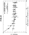
- FIG. 2 is a graph illustrating the thickness relative to plating quantity of deposits when tin-lead alloy is deposited using plating bath No. 7 (Example) and No. 11 (Comparative Example).
- the chemical or electroless plating bath used contains as main ingredients (A) a metal salt component selected from the group consisting of a water soluble tin salt, a water soluble lead salt and a mixture thereof, (B) an acid component capable of dissolving the metal salt component, and (C) a complexing agent.
- A a metal salt component selected from the group consisting of a water soluble tin salt, a water soluble lead salt and a mixture thereof
- B an acid component capable of dissolving the metal salt component
- C a complexing agent
- any water soluble tin salt may be used which can provide a stannous ion, i.e., divalent tin ion. Included are stannous oxide, stannous chloride, stannous sulfate, stannous organic sulfonates such as stannous alkane sulfonates and stannous alkanol sulfonates, stannous organic carboxylates, stannous sulfosuccinate, and stannous borofluoride.
- water soluble lead salt examples include lead chloride, lead sulfate, lead acetate, lead oxide, lead organic sulfonates such as lead methanesulfonate and lead alkanol sulfonates, and lead borofluoride.
- the metal salt components are preferably contained in amounts of about 0.5 to 30 grams/liter, especially about 1 to 20 grams/liter.
- Acid component (B) capable of dissolving these metal salts includes organic sulfonic acids, perchloric acid, fluoroboric acid, phosphoric acid, pyrophosphoric acid, condensed phosphoric acids such as polyphosphoric acids, and hydrochloric acid and a mixture of two or more of these acids.
- organic sulfonic acids are alkane sulfonic acids, hydroxyalkane sulfonic acids, benzene sulfonic acid, naphthalene sulfonic acid and substituted ones thereof in which one or more hydrogen atoms are replaced by halogen atoms, hydroxyl, alkyl, carboxyl, nitro, mercapto, amino, and sulfonate groups.
- organic sulfonic acid used herein include methanesulfonic acid, ethanesulfonic acid, propanesulfonic acid, 2-propanesulfonic acid, butanesulfonic acid, 2-butanesulfonic acid, pentanesulfonic acid, hexanesulfonic acid, decanesulfonic acid, dodecanesulfonic acid, chloropropanesulfonic acid, 2-hydroxyethane-1-sulfonic acid, 2-hydroxypropane-1-sulfonic acid, 1-hydroxypropane-2-sulfonic acid, 3-hydroxypropane-1-sulfonic acid, 2-hydroxybutane-1-sulfonic acid, 4-hydroxybutane-1-sulfonic acid, 2-hydroxypentane-1-sulfonic acid, 2-hydroxyhexane-1-sulfonic acid, 2-hydroxydecane-1-sulfonic acid, 2-hydroxydodecane-1-sulfonic acid, allys
- Complexing agent (C) includes, for example, oxalic acid, tartaric acid, citric acid, ethylenediaminetetraacetic acid (EDTA) and salts thereof, thiourea, thiourea derivatives, triethanol amine, and a mixture thereof.
- the complexing agents are preferably used in amounts of about 30 to 200 grams/liter, especially about 50 to 150 grams/liter. Too low contents of the complexing agent would allow the bath to decompose whereas too high contents of the complexing agent would lower the deposition rate.
- Preferred among the above-mentioned complexing agents are thiourea and its derivatives, which are preferably used in amounts of about 50 to 200 grams/liter, especially about 50 to 150 grams/liter.
- Exemplary of the thiourea derivatives are thioamides such as thioformamide, thioacetamide, etc.
- a reducing agent may be added to the plating bath.
- Preferred examples of the reducing agent include hypophosphorous acid, and water soluble hypophosphites such as sodium hypophosphite and potassium hypophsphite.
- the reducing agents are added in commonly used amounts, preferably from about 30 to 300 grams/liter, more preferably from about 50 to 200 grams/liter.
- the plating bath is preferably adjusted to pH 0 to 3 and maintained at temperatures of about 60 to 90°C during plating operation.
- the plating process according to the first form of the present invention is by dipping an article to be plated at least a portion of which is formed of copper or copper alloy in the above-defined plating bath, thereby depositing a coating of tin, lead or tin-lead alloy on the copper or copper alloy portion of the article.
- the copper alloy should contain more than 50% by weight of copper and include Cu-Zn, Cu-Sn, etc.
- copper ion is dissolved from the article into the plating bath simultaneously with deposition of tin, lead or tin-lead alloy. The concentration of copper ion dissolved out is analyzed at suitable intervals.
- the tin or lead salt is replenished to the bath in an amount corresponding to the copper ion increase.
- Replenishment may be made by adding the tin or lead salt directly or a solution of the salt in water or a plating solution containing the salt.
- One approach is to simply make up the tin or lead salt as the copper concentration increases.
- a certain amount of the used plating solution is discarded and a corresponding amount of a fresh plating solution is made up so as to provide the necessary replenishment of tin or lead salt.
- the plating process in the replenishment mode as mentioned above allows the plating bath to survive until copper ion builds up to a concentration of about 8 to 10 grams/liter, which corresponds to a total plating quantity of about 300 ⁇ m ⁇ dm2/liter.
- Quantitative determination of the copper ion concentration can be done by atomic absorption spectroscopy.
- the plating process according to the first form of the invention permits the plating bath to be controlled in such a manner that a tin, lead or tin-lead alloy coating can be continuously formed to a substantial thickness.
- This plating process is advantageously employed to form tin, lead or tin-lead alloy coatings on copper or copper alloy portions of electronic parts or circuits for imparting solder receptivity thereto.
- the second form of the present invention is also directed to an electroless tin, lead or tin-lead alloy plating process.
- a bath containing (A) a metal salt component selected from the group consisting of a water soluble tin salt, a water soluble lead salt, and a mixture thereof, (B) an acid capable of dissolving the salts, (C) a complexing agent preferably in the form of thiourea or a derivative thereof, and an optional reducing agent, there is added a water soluble copper salt to a fresh electroless plating bath.
- the plating process of the second form have the advantage that the bath is stable and the deposited coating is uniform due to the copper salt added to the bath.
- Components (A) to (C) and reducing agent are as previously mentioned.
- the water soluble copper salts used herein include copper sulfate, cuprous chloride, cupric chloride, copper borofluoride, cuprous oxide, cupric oxide, copper acetate, copper organic sulfonates, and copper organic carboxylates.
- the copper salts are preferably added to the fresh or make-up bath in amounts of about 0.01 to 5 grams/liter, more preferably about 0.1 to 3 grams/liter.
- the process of the first form may be combined. That is, electroless plating in the bath of the second form may be carried out while analyzing the copper ion in the bath and replenishing a water soluble tin and/or lead salt in proportion to an increase of the copper ion concentration.
- the fresh electroless tin, lead or tin-lead alloy plating bath containing the water soluble copper salt remains stable throughout its service life from the initial formulation to the end of long-term operation and thus always deposits a uniform tin, lead or tin-lead alloy film from the start which can accommodate for SMT-oriented fine pitch printed circuit boards and chip parts.
- the electroless plating processes of the first and second forms of the invention are advantageously employed in electroless plating on copper or copper alloy portions of electronic parts, typically printed circuit boards for providing solderability thereto, but are equally applicable to electroless plating on other copper and copper alloy bearing articles.
- Copper parts were successively dipped in an electroless tin-lead alloy plating bath of the following composition where chemical tin-lead alloy plating was performed at a bath temperature of 80°C.
- the copper ion concentration was analyzed at intervals by atomic absorption spectroscopy. Whenever the concentration increased by 0.5 grams/liter, the following replenishers (1) to (3) were supplied to the bath in the indicated rates.
- the deposition rate was 13 ⁇ m/15 min. and remained constant until 8 grams/liter of copper built up in the bath.
- the total plating quantity was 260 ⁇ m ⁇ dm2/liter.
- Printed circuit board test pieces having a copper circuit formed thereon were dipped in plating baths of the following composition Nos. 3 to 9 (Examples within the scope of the invention) and Nos. 10 to 12 (Comparative Examples outside the scope of the invention).
- Bath composition No. 3 to 9 Examples within the scope of the invention
- Nos. 10 to 12 Comparative Examples outside the scope of the invention.
- tin or tin-lead alloy layers were deposited on the copper circuits of the test pieces. This operation was repeated several cycles and the thickness and composition of the resulting deposits were examined at the end of each cycle.
- Methanesulfonic acid 30 g/l Stannous methanesulfonate 20 g/l Lead methanesulfonate 13 g/l Thiourea 75 g/l Sodium hypophsphite 80 g/l Citric acid 15 g/l EDTA 3 g/l Copper sulfate 0.5 g/l pH 2.0 Bath composition No.
- FIG. 1 shows the alloy composition of deposits relative to plating quantity
- FIG. 2 shows the thickness of deposits relative to plating quantity.
Landscapes
- Chemical & Material Sciences (AREA)
- General Chemical & Material Sciences (AREA)
- Chemical Kinetics & Catalysis (AREA)
- Engineering & Computer Science (AREA)
- Materials Engineering (AREA)
- Mechanical Engineering (AREA)
- Metallurgy (AREA)
- Organic Chemistry (AREA)
- Chemically Coating (AREA)
Applications Claiming Priority (2)
| Application Number | Priority Date | Filing Date | Title |
|---|---|---|---|
| JP3059642A JP2787142B2 (ja) | 1991-03-01 | 1991-03-01 | 無電解錫、鉛又はそれらの合金めっき方法 |
| JP59642/91 | 1991-03-01 |
Publications (3)
| Publication Number | Publication Date |
|---|---|
| EP0503389A2 true EP0503389A2 (de) | 1992-09-16 |
| EP0503389A3 EP0503389A3 (en) | 1993-12-29 |
| EP0503389B1 EP0503389B1 (de) | 1997-05-14 |
Family
ID=13119079
Family Applications (1)
| Application Number | Title | Priority Date | Filing Date |
|---|---|---|---|
| EP92103366A Expired - Lifetime EP0503389B1 (de) | 1991-03-01 | 1992-02-27 | Verfahren zur stromlosen Plattierung von Zinn, Blei oder Zinn-Blei-Legierung |
Country Status (6)
| Country | Link |
|---|---|
| US (1) | US5248527A (de) |
| EP (1) | EP0503389B1 (de) |
| JP (1) | JP2787142B2 (de) |
| KR (1) | KR100241090B1 (de) |
| DE (1) | DE69219645T2 (de) |
| TW (1) | TW223127B (de) |
Cited By (5)
| Publication number | Priority date | Publication date | Assignee | Title |
|---|---|---|---|---|
| DE4238765A1 (de) * | 1992-11-10 | 1994-05-11 | Stuebing Gmbh | Verfahren zur stromlosen Verzinnung von Leiterplatten und deren Verwendung |
| US5430099A (en) * | 1992-05-28 | 1995-07-04 | Aligena Ag | Immobilized buffered gels and membranes of hydroxy groups containing polymers |
| EP0915183A1 (de) * | 1997-11-07 | 1999-05-12 | ATOTECH Deutschland GmbH | Verzinnung von Kupferrohren |
| EP2182097A1 (de) * | 2008-09-22 | 2010-05-05 | Rohm and Haas Electronic Materials LLC | Wässrige Lösung zur Metalloberflächenbehandlung und Verfahren zur Hemmung von Whiskern auf einer Metalloberfläche |
| WO2011023411A1 (en) * | 2009-08-24 | 2011-03-03 | Atotech Deutschland Gmbh | Method for electroless plating of tin and tin alloys |
Families Citing this family (198)
| Publication number | Priority date | Publication date | Assignee | Title |
|---|---|---|---|---|
| DE19653765A1 (de) * | 1996-12-23 | 1998-06-25 | Km Europa Metal Ag | Innen verzinntes Kupferrohr und Verfahren zur Beschichtung eines Kupferrohrs |
| JP4558883B2 (ja) * | 2000-03-24 | 2010-10-06 | 義和 小林 | 酸性無電解錫めっき液中の銅の定量方法 |
| US6645550B1 (en) * | 2000-06-22 | 2003-11-11 | Applied Materials, Inc. | Method of treating a substrate |
| US20040131792A1 (en) * | 2001-03-22 | 2004-07-08 | Bhattacharya Raghu N. | Electroless deposition of cu-in-ga-se film |
| JP2002317275A (ja) * | 2001-04-17 | 2002-10-31 | Toto Ltd | 無電解スズめっき液の長寿命化方法 |
| US7138014B2 (en) | 2002-01-28 | 2006-11-21 | Applied Materials, Inc. | Electroless deposition apparatus |
| US6824666B2 (en) * | 2002-01-28 | 2004-11-30 | Applied Materials, Inc. | Electroless deposition method over sub-micron apertures |
| US6899816B2 (en) * | 2002-04-03 | 2005-05-31 | Applied Materials, Inc. | Electroless deposition method |
| US6905622B2 (en) * | 2002-04-03 | 2005-06-14 | Applied Materials, Inc. | Electroless deposition method |
| US6838114B2 (en) | 2002-05-24 | 2005-01-04 | Micron Technology, Inc. | Methods for controlling gas pulsing in processes for depositing materials onto micro-device workpieces |
| US6821347B2 (en) | 2002-07-08 | 2004-11-23 | Micron Technology, Inc. | Apparatus and method for depositing materials onto microelectronic workpieces |
| US6955725B2 (en) | 2002-08-15 | 2005-10-18 | Micron Technology, Inc. | Reactors with isolated gas connectors and methods for depositing materials onto micro-device workpieces |
| US6642158B1 (en) * | 2002-09-23 | 2003-11-04 | Intel Corporation | Photo-thermal induced diffusion |
| US6821909B2 (en) * | 2002-10-30 | 2004-11-23 | Applied Materials, Inc. | Post rinse to improve selective deposition of electroless cobalt on copper for ULSI application |
| US7335396B2 (en) | 2003-04-24 | 2008-02-26 | Micron Technology, Inc. | Methods for controlling mass flow rates and pressures in passageways coupled to reaction chambers and systems for depositing material onto microfeature workpieces in reaction chambers |
| US7344755B2 (en) | 2003-08-21 | 2008-03-18 | Micron Technology, Inc. | Methods and apparatus for processing microfeature workpieces; methods for conditioning ALD reaction chambers |
| US7235138B2 (en) | 2003-08-21 | 2007-06-26 | Micron Technology, Inc. | Microfeature workpiece processing apparatus and methods for batch deposition of materials on microfeature workpieces |
| US7422635B2 (en) | 2003-08-28 | 2008-09-09 | Micron Technology, Inc. | Methods and apparatus for processing microfeature workpieces, e.g., for depositing materials on microfeature workpieces |
| US7056806B2 (en) | 2003-09-17 | 2006-06-06 | Micron Technology, Inc. | Microfeature workpiece processing apparatus and methods for controlling deposition of materials on microfeature workpieces |
| US7282239B2 (en) | 2003-09-18 | 2007-10-16 | Micron Technology, Inc. | Systems and methods for depositing material onto microfeature workpieces in reaction chambers |
| US7654221B2 (en) * | 2003-10-06 | 2010-02-02 | Applied Materials, Inc. | Apparatus for electroless deposition of metals onto semiconductor substrates |
| US7827930B2 (en) | 2004-01-26 | 2010-11-09 | Applied Materials, Inc. | Apparatus for electroless deposition of metals onto semiconductor substrates |
| US7323231B2 (en) * | 2003-10-09 | 2008-01-29 | Micron Technology, Inc. | Apparatus and methods for plasma vapor deposition processes |
| US7581511B2 (en) | 2003-10-10 | 2009-09-01 | Micron Technology, Inc. | Apparatus and methods for manufacturing microfeatures on workpieces using plasma vapor processes |
| US7465358B2 (en) * | 2003-10-15 | 2008-12-16 | Applied Materials, Inc. | Measurement techniques for controlling aspects of a electroless deposition process |
| US7647886B2 (en) | 2003-10-15 | 2010-01-19 | Micron Technology, Inc. | Systems for depositing material onto workpieces in reaction chambers and methods for removing byproducts from reaction chambers |
| US20070111519A1 (en) * | 2003-10-15 | 2007-05-17 | Applied Materials, Inc. | Integrated electroless deposition system |
| US7064065B2 (en) * | 2003-10-15 | 2006-06-20 | Applied Materials, Inc. | Silver under-layers for electroless cobalt alloys |
| WO2005038084A2 (en) * | 2003-10-17 | 2005-04-28 | Applied Materials, Inc. | Selective self-initiating electroless capping of copper with cobalt-containing alloys |
| US7205233B2 (en) | 2003-11-07 | 2007-04-17 | Applied Materials, Inc. | Method for forming CoWRe alloys by electroless deposition |
| US20060003570A1 (en) * | 2003-12-02 | 2006-01-05 | Arulkumar Shanmugasundram | Method and apparatus for electroless capping with vapor drying |
| US7258892B2 (en) | 2003-12-10 | 2007-08-21 | Micron Technology, Inc. | Methods and systems for controlling temperature during microfeature workpiece processing, e.g., CVD deposition |
| US7906393B2 (en) * | 2004-01-28 | 2011-03-15 | Micron Technology, Inc. | Methods for forming small-scale capacitor structures |
| US20050230350A1 (en) * | 2004-02-26 | 2005-10-20 | Applied Materials, Inc. | In-situ dry clean chamber for front end of line fabrication |
| US7584942B2 (en) * | 2004-03-31 | 2009-09-08 | Micron Technology, Inc. | Ampoules for producing a reaction gas and systems for depositing materials onto microfeature workpieces in reaction chambers |
| US8133554B2 (en) | 2004-05-06 | 2012-03-13 | Micron Technology, Inc. | Methods for depositing material onto microfeature workpieces in reaction chambers and systems for depositing materials onto microfeature workpieces |
| US7699932B2 (en) | 2004-06-02 | 2010-04-20 | Micron Technology, Inc. | Reactors, systems and methods for depositing thin films onto microfeature workpieces |
| ES2354045T3 (es) * | 2005-02-28 | 2011-03-09 | Rohm And Haas Electronic Materials, Llc | Procedimientos con fundente mejorados. |
| WO2006102318A2 (en) | 2005-03-18 | 2006-09-28 | Applied Materials, Inc. | Electroless deposition process on a contact containing silicon or silicide |
| US7651934B2 (en) | 2005-03-18 | 2010-01-26 | Applied Materials, Inc. | Process for electroless copper deposition |
| US7867900B2 (en) | 2007-09-28 | 2011-01-11 | Applied Materials, Inc. | Aluminum contact integration on cobalt silicide junction |
| US9324576B2 (en) | 2010-05-27 | 2016-04-26 | Applied Materials, Inc. | Selective etch for silicon films |
| US10283321B2 (en) | 2011-01-18 | 2019-05-07 | Applied Materials, Inc. | Semiconductor processing system and methods using capacitively coupled plasma |
| US8771539B2 (en) | 2011-02-22 | 2014-07-08 | Applied Materials, Inc. | Remotely-excited fluorine and water vapor etch |
| US8999856B2 (en) | 2011-03-14 | 2015-04-07 | Applied Materials, Inc. | Methods for etch of sin films |
| US9064815B2 (en) | 2011-03-14 | 2015-06-23 | Applied Materials, Inc. | Methods for etch of metal and metal-oxide films |
| US8834958B2 (en) | 2011-07-08 | 2014-09-16 | The United States Of America As Represented By The Secretary Of The Army | Process of making negative electrode |
| US8771536B2 (en) | 2011-08-01 | 2014-07-08 | Applied Materials, Inc. | Dry-etch for silicon-and-carbon-containing films |
| US8679982B2 (en) | 2011-08-26 | 2014-03-25 | Applied Materials, Inc. | Selective suppression of dry-etch rate of materials containing both silicon and oxygen |
| US8679983B2 (en) | 2011-09-01 | 2014-03-25 | Applied Materials, Inc. | Selective suppression of dry-etch rate of materials containing both silicon and nitrogen |
| US8927390B2 (en) | 2011-09-26 | 2015-01-06 | Applied Materials, Inc. | Intrench profile |
| US8808563B2 (en) | 2011-10-07 | 2014-08-19 | Applied Materials, Inc. | Selective etch of silicon by way of metastable hydrogen termination |
| WO2013070436A1 (en) | 2011-11-08 | 2013-05-16 | Applied Materials, Inc. | Methods of reducing substrate dislocation during gapfill processing |
| JP6089164B2 (ja) * | 2012-03-30 | 2017-03-08 | 石原ケミカル株式会社 | スズ系メッキ液への補給方法 |
| CN102797001A (zh) * | 2012-07-11 | 2012-11-28 | 常州大学 | 基于氯化胆碱的化学镀锡溶液及其使用方法 |
| US9267739B2 (en) | 2012-07-18 | 2016-02-23 | Applied Materials, Inc. | Pedestal with multi-zone temperature control and multiple purge capabilities |
| US9373517B2 (en) | 2012-08-02 | 2016-06-21 | Applied Materials, Inc. | Semiconductor processing with DC assisted RF power for improved control |
| JP6047714B2 (ja) * | 2012-08-08 | 2016-12-21 | 石原ケミカル株式会社 | 無電解スズ系メッキ液用のペースト状スズ補給剤及び補給方法 |
| US9034770B2 (en) | 2012-09-17 | 2015-05-19 | Applied Materials, Inc. | Differential silicon oxide etch |
| US9023734B2 (en) | 2012-09-18 | 2015-05-05 | Applied Materials, Inc. | Radical-component oxide etch |
| US9390937B2 (en) | 2012-09-20 | 2016-07-12 | Applied Materials, Inc. | Silicon-carbon-nitride selective etch |
| US9132436B2 (en) | 2012-09-21 | 2015-09-15 | Applied Materials, Inc. | Chemical control features in wafer process equipment |
| US8765574B2 (en) | 2012-11-09 | 2014-07-01 | Applied Materials, Inc. | Dry etch process |
| US8969212B2 (en) | 2012-11-20 | 2015-03-03 | Applied Materials, Inc. | Dry-etch selectivity |
| US8980763B2 (en) | 2012-11-30 | 2015-03-17 | Applied Materials, Inc. | Dry-etch for selective tungsten removal |
| US9064816B2 (en) | 2012-11-30 | 2015-06-23 | Applied Materials, Inc. | Dry-etch for selective oxidation removal |
| US9111877B2 (en) | 2012-12-18 | 2015-08-18 | Applied Materials, Inc. | Non-local plasma oxide etch |
| US8921234B2 (en) | 2012-12-21 | 2014-12-30 | Applied Materials, Inc. | Selective titanium nitride etching |
| US10256079B2 (en) | 2013-02-08 | 2019-04-09 | Applied Materials, Inc. | Semiconductor processing systems having multiple plasma configurations |
| US9362130B2 (en) | 2013-03-01 | 2016-06-07 | Applied Materials, Inc. | Enhanced etching processes using remote plasma sources |
| US9040422B2 (en) | 2013-03-05 | 2015-05-26 | Applied Materials, Inc. | Selective titanium nitride removal |
| US8801952B1 (en) | 2013-03-07 | 2014-08-12 | Applied Materials, Inc. | Conformal oxide dry etch |
| US10170282B2 (en) | 2013-03-08 | 2019-01-01 | Applied Materials, Inc. | Insulated semiconductor faceplate designs |
| US20140271097A1 (en) | 2013-03-15 | 2014-09-18 | Applied Materials, Inc. | Processing systems and methods for halide scavenging |
| US8895449B1 (en) | 2013-05-16 | 2014-11-25 | Applied Materials, Inc. | Delicate dry clean |
| US9114438B2 (en) | 2013-05-21 | 2015-08-25 | Applied Materials, Inc. | Copper residue chamber clean |
| US9493879B2 (en) | 2013-07-12 | 2016-11-15 | Applied Materials, Inc. | Selective sputtering for pattern transfer |
| US9773648B2 (en) | 2013-08-30 | 2017-09-26 | Applied Materials, Inc. | Dual discharge modes operation for remote plasma |
| US8956980B1 (en) | 2013-09-16 | 2015-02-17 | Applied Materials, Inc. | Selective etch of silicon nitride |
| US8951429B1 (en) | 2013-10-29 | 2015-02-10 | Applied Materials, Inc. | Tungsten oxide processing |
| US9236265B2 (en) | 2013-11-04 | 2016-01-12 | Applied Materials, Inc. | Silicon germanium processing |
| US9576809B2 (en) | 2013-11-04 | 2017-02-21 | Applied Materials, Inc. | Etch suppression with germanium |
| US9520303B2 (en) | 2013-11-12 | 2016-12-13 | Applied Materials, Inc. | Aluminum selective etch |
| US9245762B2 (en) | 2013-12-02 | 2016-01-26 | Applied Materials, Inc. | Procedure for etch rate consistency |
| US9117855B2 (en) | 2013-12-04 | 2015-08-25 | Applied Materials, Inc. | Polarity control for remote plasma |
| US9263278B2 (en) | 2013-12-17 | 2016-02-16 | Applied Materials, Inc. | Dopant etch selectivity control |
| US9287095B2 (en) | 2013-12-17 | 2016-03-15 | Applied Materials, Inc. | Semiconductor system assemblies and methods of operation |
| US9190293B2 (en) | 2013-12-18 | 2015-11-17 | Applied Materials, Inc. | Even tungsten etch for high aspect ratio trenches |
| US9287134B2 (en) | 2014-01-17 | 2016-03-15 | Applied Materials, Inc. | Titanium oxide etch |
| US9396989B2 (en) | 2014-01-27 | 2016-07-19 | Applied Materials, Inc. | Air gaps between copper lines |
| US9293568B2 (en) | 2014-01-27 | 2016-03-22 | Applied Materials, Inc. | Method of fin patterning |
| US9385028B2 (en) | 2014-02-03 | 2016-07-05 | Applied Materials, Inc. | Air gap process |
| US9499898B2 (en) | 2014-03-03 | 2016-11-22 | Applied Materials, Inc. | Layered thin film heater and method of fabrication |
| US9299575B2 (en) | 2014-03-17 | 2016-03-29 | Applied Materials, Inc. | Gas-phase tungsten etch |
| US9299538B2 (en) | 2014-03-20 | 2016-03-29 | Applied Materials, Inc. | Radial waveguide systems and methods for post-match control of microwaves |
| US9299537B2 (en) | 2014-03-20 | 2016-03-29 | Applied Materials, Inc. | Radial waveguide systems and methods for post-match control of microwaves |
| US9136273B1 (en) | 2014-03-21 | 2015-09-15 | Applied Materials, Inc. | Flash gate air gap |
| US9903020B2 (en) | 2014-03-31 | 2018-02-27 | Applied Materials, Inc. | Generation of compact alumina passivation layers on aluminum plasma equipment components |
| US9269590B2 (en) | 2014-04-07 | 2016-02-23 | Applied Materials, Inc. | Spacer formation |
| US9309598B2 (en) | 2014-05-28 | 2016-04-12 | Applied Materials, Inc. | Oxide and metal removal |
| US9847289B2 (en) | 2014-05-30 | 2017-12-19 | Applied Materials, Inc. | Protective via cap for improved interconnect performance |
| US9378969B2 (en) | 2014-06-19 | 2016-06-28 | Applied Materials, Inc. | Low temperature gas-phase carbon removal |
| US9406523B2 (en) | 2014-06-19 | 2016-08-02 | Applied Materials, Inc. | Highly selective doped oxide removal method |
| US9425058B2 (en) | 2014-07-24 | 2016-08-23 | Applied Materials, Inc. | Simplified litho-etch-litho-etch process |
| US9159606B1 (en) | 2014-07-31 | 2015-10-13 | Applied Materials, Inc. | Metal air gap |
| US9378978B2 (en) | 2014-07-31 | 2016-06-28 | Applied Materials, Inc. | Integrated oxide recess and floating gate fin trimming |
| US9496167B2 (en) | 2014-07-31 | 2016-11-15 | Applied Materials, Inc. | Integrated bit-line airgap formation and gate stack post clean |
| US9165786B1 (en) | 2014-08-05 | 2015-10-20 | Applied Materials, Inc. | Integrated oxide and nitride recess for better channel contact in 3D architectures |
| US9659753B2 (en) | 2014-08-07 | 2017-05-23 | Applied Materials, Inc. | Grooved insulator to reduce leakage current |
| US9553102B2 (en) | 2014-08-19 | 2017-01-24 | Applied Materials, Inc. | Tungsten separation |
| US9355856B2 (en) | 2014-09-12 | 2016-05-31 | Applied Materials, Inc. | V trench dry etch |
| US9368364B2 (en) | 2014-09-24 | 2016-06-14 | Applied Materials, Inc. | Silicon etch process with tunable selectivity to SiO2 and other materials |
| US9478434B2 (en) | 2014-09-24 | 2016-10-25 | Applied Materials, Inc. | Chlorine-based hardmask removal |
| US9613822B2 (en) | 2014-09-25 | 2017-04-04 | Applied Materials, Inc. | Oxide etch selectivity enhancement |
| US9355922B2 (en) | 2014-10-14 | 2016-05-31 | Applied Materials, Inc. | Systems and methods for internal surface conditioning in plasma processing equipment |
| US9966240B2 (en) | 2014-10-14 | 2018-05-08 | Applied Materials, Inc. | Systems and methods for internal surface conditioning assessment in plasma processing equipment |
| US11637002B2 (en) | 2014-11-26 | 2023-04-25 | Applied Materials, Inc. | Methods and systems to enhance process uniformity |
| US9299583B1 (en) | 2014-12-05 | 2016-03-29 | Applied Materials, Inc. | Aluminum oxide selective etch |
| US10573496B2 (en) | 2014-12-09 | 2020-02-25 | Applied Materials, Inc. | Direct outlet toroidal plasma source |
| US10224210B2 (en) | 2014-12-09 | 2019-03-05 | Applied Materials, Inc. | Plasma processing system with direct outlet toroidal plasma source |
| US9502258B2 (en) | 2014-12-23 | 2016-11-22 | Applied Materials, Inc. | Anisotropic gap etch |
| US9343272B1 (en) | 2015-01-08 | 2016-05-17 | Applied Materials, Inc. | Self-aligned process |
| US11257693B2 (en) | 2015-01-09 | 2022-02-22 | Applied Materials, Inc. | Methods and systems to improve pedestal temperature control |
| US9373522B1 (en) | 2015-01-22 | 2016-06-21 | Applied Mateials, Inc. | Titanium nitride removal |
| US9449846B2 (en) | 2015-01-28 | 2016-09-20 | Applied Materials, Inc. | Vertical gate separation |
| US20160225652A1 (en) | 2015-02-03 | 2016-08-04 | Applied Materials, Inc. | Low temperature chuck for plasma processing systems |
| US9728437B2 (en) | 2015-02-03 | 2017-08-08 | Applied Materials, Inc. | High temperature chuck for plasma processing systems |
| US9881805B2 (en) | 2015-03-02 | 2018-01-30 | Applied Materials, Inc. | Silicon selective removal |
| US9691645B2 (en) | 2015-08-06 | 2017-06-27 | Applied Materials, Inc. | Bolted wafer chuck thermal management systems and methods for wafer processing systems |
| US9741593B2 (en) | 2015-08-06 | 2017-08-22 | Applied Materials, Inc. | Thermal management systems and methods for wafer processing systems |
| US9349605B1 (en) | 2015-08-07 | 2016-05-24 | Applied Materials, Inc. | Oxide etch selectivity systems and methods |
| US10504700B2 (en) | 2015-08-27 | 2019-12-10 | Applied Materials, Inc. | Plasma etching systems and methods with secondary plasma injection |
| US10522371B2 (en) | 2016-05-19 | 2019-12-31 | Applied Materials, Inc. | Systems and methods for improved semiconductor etching and component protection |
| US10504754B2 (en) | 2016-05-19 | 2019-12-10 | Applied Materials, Inc. | Systems and methods for improved semiconductor etching and component protection |
| US9865484B1 (en) | 2016-06-29 | 2018-01-09 | Applied Materials, Inc. | Selective etch using material modification and RF pulsing |
| US10062575B2 (en) | 2016-09-09 | 2018-08-28 | Applied Materials, Inc. | Poly directional etch by oxidation |
| US10629473B2 (en) | 2016-09-09 | 2020-04-21 | Applied Materials, Inc. | Footing removal for nitride spacer |
| US10546729B2 (en) | 2016-10-04 | 2020-01-28 | Applied Materials, Inc. | Dual-channel showerhead with improved profile |
| US10062585B2 (en) | 2016-10-04 | 2018-08-28 | Applied Materials, Inc. | Oxygen compatible plasma source |
| US9721789B1 (en) | 2016-10-04 | 2017-08-01 | Applied Materials, Inc. | Saving ion-damaged spacers |
| US9934942B1 (en) | 2016-10-04 | 2018-04-03 | Applied Materials, Inc. | Chamber with flow-through source |
| US10062579B2 (en) | 2016-10-07 | 2018-08-28 | Applied Materials, Inc. | Selective SiN lateral recess |
| US9947549B1 (en) | 2016-10-10 | 2018-04-17 | Applied Materials, Inc. | Cobalt-containing material removal |
| US10163696B2 (en) | 2016-11-11 | 2018-12-25 | Applied Materials, Inc. | Selective cobalt removal for bottom up gapfill |
| US9768034B1 (en) | 2016-11-11 | 2017-09-19 | Applied Materials, Inc. | Removal methods for high aspect ratio structures |
| US10026621B2 (en) | 2016-11-14 | 2018-07-17 | Applied Materials, Inc. | SiN spacer profile patterning |
| US10242908B2 (en) | 2016-11-14 | 2019-03-26 | Applied Materials, Inc. | Airgap formation with damage-free copper |
| US10566206B2 (en) | 2016-12-27 | 2020-02-18 | Applied Materials, Inc. | Systems and methods for anisotropic material breakthrough |
| US10431429B2 (en) | 2017-02-03 | 2019-10-01 | Applied Materials, Inc. | Systems and methods for radial and azimuthal control of plasma uniformity |
| US10403507B2 (en) | 2017-02-03 | 2019-09-03 | Applied Materials, Inc. | Shaped etch profile with oxidation |
| US10043684B1 (en) | 2017-02-06 | 2018-08-07 | Applied Materials, Inc. | Self-limiting atomic thermal etching systems and methods |
| US10319739B2 (en) | 2017-02-08 | 2019-06-11 | Applied Materials, Inc. | Accommodating imperfectly aligned memory holes |
| US10943834B2 (en) | 2017-03-13 | 2021-03-09 | Applied Materials, Inc. | Replacement contact process |
| US10319649B2 (en) | 2017-04-11 | 2019-06-11 | Applied Materials, Inc. | Optical emission spectroscopy (OES) for remote plasma monitoring |
| JP7176860B6 (ja) | 2017-05-17 | 2022-12-16 | アプライド マテリアルズ インコーポレイテッド | 前駆体の流れを改善する半導体処理チャンバ |
| US11276590B2 (en) | 2017-05-17 | 2022-03-15 | Applied Materials, Inc. | Multi-zone semiconductor substrate supports |
| US11276559B2 (en) | 2017-05-17 | 2022-03-15 | Applied Materials, Inc. | Semiconductor processing chamber for multiple precursor flow |
| US10497579B2 (en) | 2017-05-31 | 2019-12-03 | Applied Materials, Inc. | Water-free etching methods |
| US10049891B1 (en) | 2017-05-31 | 2018-08-14 | Applied Materials, Inc. | Selective in situ cobalt residue removal |
| US10920320B2 (en) | 2017-06-16 | 2021-02-16 | Applied Materials, Inc. | Plasma health determination in semiconductor substrate processing reactors |
| US10541246B2 (en) | 2017-06-26 | 2020-01-21 | Applied Materials, Inc. | 3D flash memory cells which discourage cross-cell electrical tunneling |
| US10858748B2 (en) | 2017-06-30 | 2020-12-08 | Apollo Energy Systems, Inc. | Method of manufacturing hybrid metal foams |
| US10727080B2 (en) | 2017-07-07 | 2020-07-28 | Applied Materials, Inc. | Tantalum-containing material removal |
| US10541184B2 (en) | 2017-07-11 | 2020-01-21 | Applied Materials, Inc. | Optical emission spectroscopic techniques for monitoring etching |
| US10354889B2 (en) | 2017-07-17 | 2019-07-16 | Applied Materials, Inc. | Non-halogen etching of silicon-containing materials |
| US10170336B1 (en) | 2017-08-04 | 2019-01-01 | Applied Materials, Inc. | Methods for anisotropic control of selective silicon removal |
| US10043674B1 (en) | 2017-08-04 | 2018-08-07 | Applied Materials, Inc. | Germanium etching systems and methods |
| US10297458B2 (en) | 2017-08-07 | 2019-05-21 | Applied Materials, Inc. | Process window widening using coated parts in plasma etch processes |
| US10283324B1 (en) | 2017-10-24 | 2019-05-07 | Applied Materials, Inc. | Oxygen treatment for nitride etching |
| US10128086B1 (en) | 2017-10-24 | 2018-11-13 | Applied Materials, Inc. | Silicon pretreatment for nitride removal |
| US10256112B1 (en) | 2017-12-08 | 2019-04-09 | Applied Materials, Inc. | Selective tungsten removal |
| US10903054B2 (en) | 2017-12-19 | 2021-01-26 | Applied Materials, Inc. | Multi-zone gas distribution systems and methods |
| US11328909B2 (en) | 2017-12-22 | 2022-05-10 | Applied Materials, Inc. | Chamber conditioning and removal processes |
| US10854426B2 (en) | 2018-01-08 | 2020-12-01 | Applied Materials, Inc. | Metal recess for semiconductor structures |
| US10679870B2 (en) | 2018-02-15 | 2020-06-09 | Applied Materials, Inc. | Semiconductor processing chamber multistage mixing apparatus |
| US10964512B2 (en) | 2018-02-15 | 2021-03-30 | Applied Materials, Inc. | Semiconductor processing chamber multistage mixing apparatus and methods |
| TWI766433B (zh) | 2018-02-28 | 2022-06-01 | 美商應用材料股份有限公司 | 形成氣隙的系統及方法 |
| US10593560B2 (en) | 2018-03-01 | 2020-03-17 | Applied Materials, Inc. | Magnetic induction plasma source for semiconductor processes and equipment |
| US10319600B1 (en) | 2018-03-12 | 2019-06-11 | Applied Materials, Inc. | Thermal silicon etch |
| US10497573B2 (en) | 2018-03-13 | 2019-12-03 | Applied Materials, Inc. | Selective atomic layer etching of semiconductor materials |
| US10573527B2 (en) | 2018-04-06 | 2020-02-25 | Applied Materials, Inc. | Gas-phase selective etching systems and methods |
| US10490406B2 (en) | 2018-04-10 | 2019-11-26 | Appled Materials, Inc. | Systems and methods for material breakthrough |
| US10699879B2 (en) | 2018-04-17 | 2020-06-30 | Applied Materials, Inc. | Two piece electrode assembly with gap for plasma control |
| CN108495468A (zh) * | 2018-04-25 | 2018-09-04 | 佛山聚晨知识产权运营有限公司 | 一种印制电路板智能制造工艺 |
| US10886137B2 (en) | 2018-04-30 | 2021-01-05 | Applied Materials, Inc. | Selective nitride removal |
| US10872778B2 (en) | 2018-07-06 | 2020-12-22 | Applied Materials, Inc. | Systems and methods utilizing solid-phase etchants |
| US10755941B2 (en) | 2018-07-06 | 2020-08-25 | Applied Materials, Inc. | Self-limiting selective etching systems and methods |
| US10672642B2 (en) | 2018-07-24 | 2020-06-02 | Applied Materials, Inc. | Systems and methods for pedestal configuration |
| US11049755B2 (en) | 2018-09-14 | 2021-06-29 | Applied Materials, Inc. | Semiconductor substrate supports with embedded RF shield |
| US10892198B2 (en) | 2018-09-14 | 2021-01-12 | Applied Materials, Inc. | Systems and methods for improved performance in semiconductor processing |
| US11062887B2 (en) | 2018-09-17 | 2021-07-13 | Applied Materials, Inc. | High temperature RF heater pedestals |
| US11417534B2 (en) | 2018-09-21 | 2022-08-16 | Applied Materials, Inc. | Selective material removal |
| US11682560B2 (en) | 2018-10-11 | 2023-06-20 | Applied Materials, Inc. | Systems and methods for hafnium-containing film removal |
| US11121002B2 (en) | 2018-10-24 | 2021-09-14 | Applied Materials, Inc. | Systems and methods for etching metals and metal derivatives |
| US11437242B2 (en) | 2018-11-27 | 2022-09-06 | Applied Materials, Inc. | Selective removal of silicon-containing materials |
| US11721527B2 (en) | 2019-01-07 | 2023-08-08 | Applied Materials, Inc. | Processing chamber mixing systems |
| US10920319B2 (en) | 2019-01-11 | 2021-02-16 | Applied Materials, Inc. | Ceramic showerheads with conductive electrodes |
| CN112930041A (zh) * | 2021-01-29 | 2021-06-08 | 深圳市强达电路有限公司 | 一种二次蚀刻印制电路板的制作方法 |
Family Cites Families (11)
| Publication number | Priority date | Publication date | Assignee | Title |
|---|---|---|---|---|
| US2230602A (en) * | 1938-03-31 | 1941-02-04 | Battelle Memorial Institute | Method of coating metals with lead |
| GB1058210A (en) * | 1965-12-20 | 1967-02-08 | Shipley Co | Tin coating of metallic surfaces by immersion |
| US3689292A (en) * | 1970-12-07 | 1972-09-05 | John M Preston | Tin immersion plating bath and method |
| JPS5057927A (de) * | 1973-09-25 | 1975-05-20 | ||
| US4194913A (en) * | 1975-05-06 | 1980-03-25 | Amp Incorporated | Electroless tin and tin-lead alloy plating baths |
| US4093466A (en) * | 1975-05-06 | 1978-06-06 | Amp Incorporated | Electroless tin and tin-lead alloy plating baths |
| USRE30434E (en) * | 1978-12-21 | 1980-11-11 | Amp Incorporated | Electroless tin and tin-lead alloy plating baths |
| US4234631A (en) * | 1979-07-20 | 1980-11-18 | Amp Incorporated | Method for immersion deposition of tin and tin-lead alloys |
| JPS56112496A (en) * | 1980-02-05 | 1981-09-04 | Mitsubishi Electric Corp | Plating method |
| JPS575854A (en) * | 1980-06-12 | 1982-01-12 | Fuji Electric Co Ltd | Production of tin-plated article |
| US5143544A (en) * | 1990-06-04 | 1992-09-01 | Shipley Company Inc. | Tin lead plating solution |
-
1991
- 1991-03-01 JP JP3059642A patent/JP2787142B2/ja not_active Expired - Lifetime
-
1992
- 1992-02-25 TW TW081101408A patent/TW223127B/zh active
- 1992-02-27 DE DE69219645T patent/DE69219645T2/de not_active Expired - Fee Related
- 1992-02-27 EP EP92103366A patent/EP0503389B1/de not_active Expired - Lifetime
- 1992-02-28 US US07/843,015 patent/US5248527A/en not_active Expired - Fee Related
- 1992-03-02 KR KR1019920003429A patent/KR100241090B1/ko not_active Expired - Fee Related
Cited By (11)
| Publication number | Priority date | Publication date | Assignee | Title |
|---|---|---|---|---|
| US5430099A (en) * | 1992-05-28 | 1995-07-04 | Aligena Ag | Immobilized buffered gels and membranes of hydroxy groups containing polymers |
| DE4238765A1 (de) * | 1992-11-10 | 1994-05-11 | Stuebing Gmbh | Verfahren zur stromlosen Verzinnung von Leiterplatten und deren Verwendung |
| EP0915183A1 (de) * | 1997-11-07 | 1999-05-12 | ATOTECH Deutschland GmbH | Verzinnung von Kupferrohren |
| DE19749382A1 (de) * | 1997-11-07 | 1999-05-27 | Atotech Deutschland Gmbh | Verzinnung von Kupferrohren |
| EP2182097A1 (de) * | 2008-09-22 | 2010-05-05 | Rohm and Haas Electronic Materials LLC | Wässrige Lösung zur Metalloberflächenbehandlung und Verfahren zur Hemmung von Whiskern auf einer Metalloberfläche |
| US8591638B2 (en) | 2008-09-22 | 2013-11-26 | Rohm And Haas Electronic Materials Llc | Metal surface treatment aqueous solution and method for inhibiting whiskers on a metal surface |
| US9200168B2 (en) | 2008-09-22 | 2015-12-01 | Rohm And Haas Electronic Materials Llc | Metal surface treatment aqueous solution and method for inhibiting whiskers on a metal surface |
| WO2011023411A1 (en) * | 2009-08-24 | 2011-03-03 | Atotech Deutschland Gmbh | Method for electroless plating of tin and tin alloys |
| EP2298960A1 (de) * | 2009-08-24 | 2011-03-23 | ATOTECH Deutschland GmbH | Verfahren zum stromlosen Abscheiden von Zinn und Zinnlegierungen |
| CN102482781A (zh) * | 2009-08-24 | 2012-05-30 | 安美特德国有限公司 | 锡和锡合金的无电镀覆方法 |
| US9458541B2 (en) | 2009-08-24 | 2016-10-04 | Atotech Deutschland Gmbh | Method for electroless plating of tin and tin alloys |
Also Published As
| Publication number | Publication date |
|---|---|
| KR100241090B1 (ko) | 2000-03-02 |
| JPH04276081A (ja) | 1992-10-01 |
| KR920018241A (ko) | 1992-10-21 |
| DE69219645D1 (de) | 1997-06-19 |
| DE69219645T2 (de) | 1997-12-18 |
| EP0503389A3 (en) | 1993-12-29 |
| JP2787142B2 (ja) | 1998-08-13 |
| EP0503389B1 (de) | 1997-05-14 |
| TW223127B (de) | 1994-05-01 |
| US5248527A (en) | 1993-09-28 |
Similar Documents
| Publication | Publication Date | Title |
|---|---|---|
| EP0503389B1 (de) | Verfahren zur stromlosen Plattierung von Zinn, Blei oder Zinn-Blei-Legierung | |
| EP0520421B1 (de) | Bad zur stromlosen Beschichtung mit einer Zinn-Blei-Legierung | |
| US4424241A (en) | Electroless palladium process | |
| EP2494094B1 (de) | Zinn-silber-tauchplattierung bei der herstellung von elektronik | |
| US5266103A (en) | Bath and method for the electroless plating of tin and tin-lead alloy | |
| CA1081406A (en) | Electroless metal plating | |
| US5160422A (en) | Bath for immersion plating tin-lead alloys | |
| US4816070A (en) | Use of immersion tin and alloys as a bonding medium for multilayer circuits | |
| US5147454A (en) | Electrolessly solder plating composition | |
| US4913787A (en) | Gold plating bath and method | |
| EP3276046B1 (de) | Plattierungslösung mit verwendung von ammoniumsalz | |
| JP2009191335A (ja) | めっき液及び電子部品 | |
| EP3276045B1 (de) | Plattierungslösung mit phosphoniumsalz | |
| EP3276047B1 (de) | Plattierungslösung mit sulfoniumsalz | |
| US20040258847A1 (en) | Method of measuring component loss | |
| US5169692A (en) | Tin lead process | |
| JP2518118B2 (ja) | 無電解錫又は錫・鉛合金めっき液及び無電解錫又は錫・鉛合金めっき方法 | |
| US5334240A (en) | Aqueous acidic tin-lead immersion plating bath containing weak acid and weak base | |
| JPH05222568A (ja) | メッキ液組成物 | |
| JP2873751B2 (ja) | 無電解錫又は錫・鉛合金めっき液及び無電解錫又は錫・鉛合金めっき方法 | |
| JP2770639B2 (ja) | 無電解錫又は錫・鉛合金めっき方法 | |
| JP2757708B2 (ja) | 無電解錫・鉛合金めっき方法 | |
| CN110592624B (zh) | 一种含有复配磺酸盐光亮剂的pcb板银电镀液 | |
| JPH0250990B2 (de) | ||
| JPH05186878A (ja) | 無電解錫及び無電解錫−鉛合金メッキ浴 |
Legal Events
| Date | Code | Title | Description |
|---|---|---|---|
| PUAI | Public reference made under article 153(3) epc to a published international application that has entered the european phase |
Free format text: ORIGINAL CODE: 0009012 |
|
| AK | Designated contracting states |
Kind code of ref document: A2 Designated state(s): DE FR GB IT NL |
|
| PUAL | Search report despatched |
Free format text: ORIGINAL CODE: 0009013 |
|
| AK | Designated contracting states |
Kind code of ref document: A3 Designated state(s): DE FR GB IT NL |
|
| 17P | Request for examination filed |
Effective date: 19940125 |
|
| 17Q | First examination report despatched |
Effective date: 19950227 |
|
| GRAG | Despatch of communication of intention to grant |
Free format text: ORIGINAL CODE: EPIDOS AGRA |
|
| GRAH | Despatch of communication of intention to grant a patent |
Free format text: ORIGINAL CODE: EPIDOS IGRA |
|
| GRAH | Despatch of communication of intention to grant a patent |
Free format text: ORIGINAL CODE: EPIDOS IGRA |
|
| GRAA | (expected) grant |
Free format text: ORIGINAL CODE: 0009210 |
|
| AK | Designated contracting states |
Kind code of ref document: B1 Designated state(s): DE FR GB IT NL |
|
| PG25 | Lapsed in a contracting state [announced via postgrant information from national office to epo] |
Ref country code: IT Free format text: LAPSE BECAUSE OF FAILURE TO SUBMIT A TRANSLATION OF THE DESCRIPTION OR TO PAY THE FEE WITHIN THE PRE;WARNING: LAPSES OF ITALIAN PATENTS WITH EFFECTIVE DATE BEFORE 2007 MAY HAVE OCCURRED AT ANY TIME BEFORE 2007. THE CORRECT EFFECTIVE DATE MAY BE DIFFERENT FROM THE ONE RECORDED.SCRIBED TIME-LIMIT Effective date: 19970514 |
|
| REF | Corresponds to: |
Ref document number: 69219645 Country of ref document: DE Date of ref document: 19970619 |
|
| ET | Fr: translation filed | ||
| PLBE | No opposition filed within time limit |
Free format text: ORIGINAL CODE: 0009261 |
|
| STAA | Information on the status of an ep patent application or granted ep patent |
Free format text: STATUS: NO OPPOSITION FILED WITHIN TIME LIMIT |
|
| 26N | No opposition filed | ||
| REG | Reference to a national code |
Ref country code: GB Ref legal event code: IF02 |
|
| PGFP | Annual fee paid to national office [announced via postgrant information from national office to epo] |
Ref country code: FR Payment date: 20020212 Year of fee payment: 11 |
|
| PGFP | Annual fee paid to national office [announced via postgrant information from national office to epo] |
Ref country code: DE Payment date: 20020222 Year of fee payment: 11 |
|
| PGFP | Annual fee paid to national office [announced via postgrant information from national office to epo] |
Ref country code: GB Payment date: 20020227 Year of fee payment: 11 |
|
| PGFP | Annual fee paid to national office [announced via postgrant information from national office to epo] |
Ref country code: NL Payment date: 20020228 Year of fee payment: 11 |
|
| PG25 | Lapsed in a contracting state [announced via postgrant information from national office to epo] |
Ref country code: GB Free format text: LAPSE BECAUSE OF NON-PAYMENT OF DUE FEES Effective date: 20030227 |
|
| PG25 | Lapsed in a contracting state [announced via postgrant information from national office to epo] |
Ref country code: NL Free format text: LAPSE BECAUSE OF NON-PAYMENT OF DUE FEES Effective date: 20030901 |
|
| PG25 | Lapsed in a contracting state [announced via postgrant information from national office to epo] |
Ref country code: DE Free format text: LAPSE BECAUSE OF NON-PAYMENT OF DUE FEES Effective date: 20030902 |
|
| GBPC | Gb: european patent ceased through non-payment of renewal fee | ||
| PG25 | Lapsed in a contracting state [announced via postgrant information from national office to epo] |
Ref country code: FR Free format text: LAPSE BECAUSE OF NON-PAYMENT OF DUE FEES Effective date: 20031031 |
|
| NLV4 | Nl: lapsed or anulled due to non-payment of the annual fee |
Effective date: 20030901 |
|
| REG | Reference to a national code |
Ref country code: FR Ref legal event code: ST |