EP0503671A2 - Volladdierer - Google Patents
Volladdierer Download PDFInfo
- Publication number
- EP0503671A2 EP0503671A2 EP92104414A EP92104414A EP0503671A2 EP 0503671 A2 EP0503671 A2 EP 0503671A2 EP 92104414 A EP92104414 A EP 92104414A EP 92104414 A EP92104414 A EP 92104414A EP 0503671 A2 EP0503671 A2 EP 0503671A2
- Authority
- EP
- European Patent Office
- Prior art keywords
- data
- bit
- exclusive
- signal
- carry
- Prior art date
- Legal status (The legal status is an assumption and is not a legal conclusion. Google has not performed a legal analysis and makes no representation as to the accuracy of the status listed.)
- Withdrawn
Links
Images
Classifications
-
- G—PHYSICS
- G06—COMPUTING OR CALCULATING; COUNTING
- G06F—ELECTRIC DIGITAL DATA PROCESSING
- G06F7/00—Methods or arrangements for processing data by operating upon the order or content of the data handled
- G06F7/38—Methods or arrangements for performing computations using exclusively denominational number representation, e.g. using binary, ternary, decimal representation
- G06F7/48—Methods or arrangements for performing computations using exclusively denominational number representation, e.g. using binary, ternary, decimal representation using non-contact-making devices, e.g. tube, solid state device; using unspecified devices
- G06F7/50—Adding; Subtracting
- G06F7/501—Half or full adders, i.e. basic adder cells for one denomination
- G06F7/503—Half or full adders, i.e. basic adder cells for one denomination using carry switching, i.e. the incoming carry being connected directly, or only via an inverter, to the carry output under control of a carry propagate signal
Definitions
- the present invention relates to a full adder, and more specifically to a full adder receiving one-bit inputs of addend, augend and carry data, and capable of generating a one-bit sum output and one-bit carry output at a high processing speed.
- One typical conventional full adder includes a first exclusive-OR circuit receiving a first one-bit input data and a second one-bit input data, and a second exclusive-OR circuit receiving an output of the first exclusive-OR circuit and a one-bit catty-in data so as to generate a one-bit sum output.
- the conventional full adder also includes a first AND circuit receiving the first one-bit input data and the second one-bit input data, a second AND circuit receiving an output of the first exclusive-OR circuit and the one-bit carry-in data, and an OR circuit receiving outputs of the first and second AND circuit for generating a one-bit carry-out data.
- Another object of the present invention is to provide a full adder having an operation speed remarkably higher than the conventional one.
- a full adder receiving a first one-bit input data, a second one-bit input data and a one-bit carry-in data and generating a one-bit sum output and a one-bit carry-out data
- the full adder comprising a first circuit receiving the first one-bit input data and the second one-bit input data for generating an exclusive-OR signal, a second circuit receiving the first one-bit input data and the second one-bit input data for generating an exclusive-NOR signal, a third circuit receiving the exclusive-OR signal, the exclusive-NOR signal and the one-bit carry-in data for selectively outputting, as the one-bit sum data, either the one-bit carry-in data or a NOT signal of the one-bit carry-in data in accordance with the exclusive-OR signal, and a fourth circuit receiving the exclusive-OR signal, the exclusive-NOR signal, the one-bit carry-in data and one of the first one-bit input data and the second one-bit input data for selective
- the third and fourth circuits operates on the basis of the exclusive-OR and the exclusive-NOR between the first one-bit input data and the second one-bit input data, so as to perform their switching function to the effect that the one-bit sum data is selectively given by either the carry-in data and the NOT signal of the carry-in data, and the one-bit carry-out data is selectively given by either the one-bit carry-in data or the one of the first one-bit input data and the second one-bit input data. Therefore, the number of logic gates through which the input signals have to pass is remarkably decreased, and accordingly, the full addition operation can be performed at a high speed.
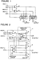
- FIG. 1 there is shown a logic block diagram of a first embodiment of the full adder in accordance with the present invention.
- the first embodiment includes an exclusive-OR circuit 4 receiving a first one-bit input data "A” and a second one-bit input data "B” supplied through first and second input terminals 1 and 2, respectively.
- This exclusive-OR circuit generates an exclusive-OR signal "X”.
- an exclusive-NOR circuit 5 receives the first one-bit input data "A” and the second one-bit input data "B” for generating an exclusive-NOR signal "Y”.
- the exclusive-OR signal "X” , the exclusive-NOR signal "Y” and a one-bit carry-in data "CI” supplied through a third input terminal 3 are supplied to a first switching circuit 6, which generates a one-bit sum data "S" to a first output terminal 8.
- the exclusive-OR signal "X”, the exclusive-NOR signal “Y”, the one-bit carry-in data "CI” and one of the first one-bit input data "A” and the second one-bit input data "B” (the second one-bit input data "B” in the shown embodiment) are supplied to a second switching circuit 7, which generates a one-bit carry-out data "CO" to a second output terminal 9.
- the output "X" of the exclusive-OR circuit 4 is “1"
- the output "Y” of the exclusive-NOR circuit 5 is "0”. If the exclusive-OR signal "X” and the exclusive-NOR signal "Y” are supplied to the first and second switching circuits 6 and 7, the first switching circuit 6 operates to make the one-bit sum output data "S” consistent with a NOT signal of the carry-in data "CI”, and the second switching circuit 7 operates to make the one-bit carry-out data "CO” consistent with the carry-in data "CI”.
- FIG 2 there is shown a logic circuit diagram of a second embodiment of the full adder in accordance with the present invention for illustrating a detailed structure of the two switching circuits.
- elements corresponding to those shown in Figure 1 are given the same Reference Numerals, and explanation thereof will be omitted.
- the first switching circuit 6 includes a transfer gate 15 connected between the input terminal 3 and the output terminal 8.
- This transfer gate 15 is composed of an N-channel MOSFET (metal-oxide-semiconductor field effect transistor) 15A and a P-channel MOSFET 15B, which are connected in parallel to each other.
- the first switching circuit 6 also includes a pair of P-channel MOSFETs 17 and 18 connected in series between the output terminal 8 and a voltage supply terminal V DD , and a pair of N-channel MOSFETs 19 and 20 connected in series between the output terminal 8 and a ground GND.
- the exclusive-OR signal "X" of the exclusive-OR circuit 4 is connected to a gate of the P-channel MOSFET 15B of the transfer gate 15 and a gate of the N-channel MOSFET 19.
- the exclusive-NOR signal “Y” of the exclusive-NOR circuit 5 is connected to a gate of the N-channel MOSFET 15A of the transfer gate 15 and a gate of the P-channel MOSFET 18.
- the carry-in signal "CI” is connected to gates of the P-channel MOSFET 17 and the N-channel MOSFET 20.
- the transfer gate 15 is controlled by the exclusive-OR signal "X" of the exclusive-OR circuit 4 and the exclusive-NOR signal "Y" of the exclusive-NOR circuit 5, so as to control whether or not the carry-in data "CI” is outputted directly to the first output terminal 8 for the sum output data "S".
- the transfer gate 15 is opened, since the P-channel MOSFET 18 and the N-channel MOSFET 19 are turned off, the carry-in data "CI" is outputted directly to the first output terminal 8 for the sum output data "S".
- the second switching circuit 7 includes a transfer gate 16 connected between the input terminal 3 and the output terminal 9.
- This transfer gate 15 is composed of an N-channel MOSFET 16A and a P-channel MOSFET 16B connected in parallel to each other.
- the second switching circuit 7 also includes a P-channel MOSFET 21 connected between the output terminal 9 and the input terminal 2 for the second input data "B", and an N-channel MOSFET 22 connected between the output terminal 9 and the input terminal 2 for the second input data "B".
- the exclusive-OR signal "X" of the exclusive-OR circuit 4 is connected to a gate of the N-channel MOSFET 16A of the transfer gate 16 and a gate of the P-channel MOSFET 21.
- the exclusive-NOR signal "Y" of the exclusive-NOR circuit 5 is connected to a gate of the P-channel MOSFET 16B of the transfer gate 16 and a gate of the N-channel MOSFET 22.
- the transfer gate 16 is controlled by the exclusive-OR signal "X" and the exclusive-NOR signal "Y", so as to control whether or not the carry-in data "CI" is outputted directly to the first output terminal 9 for the carry-out data "CO".
- the transfer gate 16 is opened, the P-channel MOSFET 21 and the N-channel MOSFET 22 are turned off, and the carry-in data "CI" is outputted to the second output terminal 9 for the carry-out data "CO".
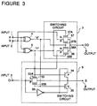
- FIG 3 there is shown a logic circuit diagram of a third embodiment of the full adder in accordance with the present invention for illustrating another detailed structure of the two switching circuits.
- elements corresponding to those shown in Figure 1 are given the same Reference Numerals, and explanation thereof will be omitted.
- the first switching circuit 6 shown in Figure 3 includes a transfer gate 33 connected between the input terminal 3 and the output terminal 8.
- This transfer gate 33 is composed of an N-channel MOSFET 33A and a P-channel MOSFET 33B connected in parallel to each other.
- a P-channel MOSFET 34 is connected between the output terminal 8 and an output of the inverter 36 having an input connected to the input terminal 3 for the carry-in signal "CI".
- An N-channel MOSFET 35 is connected between the output terminal 8 and the output of an inverter 36.
- the exclusive-OR signal "X" of the exclusive-OR circuit 4 is connected to a gate of the P-channel MOSFET 33B of the transfer gate 33 and a gate of the N-channel MOSFET 35.
- the exclusive-NOR signal "Y" of the exclusive-NOR circuit 5 is connected to a gate of the N-channel MOSFET 33A of the transfer gate 33 and a gate of the P-channel MOSFET 34.
- the transfer gate 33 is controlled by the exclusive-OR signal "X" of the exclusive-OR circuit 4 and the exclusive-NOR signal "Y" of the exclusive-NOR circuit 5, so as to control whether or not the carry-in data "CI” is outputted directly to the first output terminal 8 for the sum output data "S".
- the transfer gate 33 is opened, since the P-channel MOSFET 34 and the N-channel MOSFET 35 are turned off, the carry-in data "CI" is outputted directly to the first output terminal 8 for the sum output data "S".
- the second switching circuit 7 shown in Figure 3 includes a transfer gate 37 connected between the input terminal 2 and the output terminal 9, and another transfer gate 38 connected between the input terminal 3 and the output terminal 9.
- Each of the transfer gates 37 and 38 is composed of an N-channel MOSFET and a P-channel MOSFET connected in parallel to each other.
- the exclusive-OR signal "X" of the exclusive-OR circuit 4 is connected to a gate of a P-channel MOSFET 37B of the transfer gate 37 and a gate of an N-channel MOSFET 38A of the transfer gate 38.
- the exclusive-NOR signal "Y" of the exclusive-NOR circuit 5 is connected to a gate of an N-channel MOSFET 37A of the transfer gate 37 and a gate of a P-channel MOSFET 38B of the transfer gate 38.
- the transfer gate 37 is controlled by the exclusive-OR signal "X" of the exclusive-OR circuit 4 and the exclusive-NOR signal "Y" of the exclusive-NOR circuit 5, so as to control whether or not the second input data "B" is supplied directly to the first output terminal 9 for the carry-out data "CO".
- the transfer gate 38 is controlled by the exclusive-OR signal "X', of the exclusive-OR circuit 4 and the exclusive-NOR signal "Y" of the exclusive-NOR circuit 5, so as to control whether or not the carry-in data "CI" is supplied directly to the first output terminal 9.
- the two switching circuits operate on the basis of the exclusive-OR and the exclusive-NOR between the first one-bit input data and the second one-bit input data, so as to perform their switching function to the effect that the one-bit sum data is selectively given by either the carry-in data and the NOT signal of the carry-in data, and the carry-out data is selectively given by either the carry-in data or the one of the first input data and the second input data. Therefore, the number of logic gates through which the input signals have to pass is remarkably decreased, and accordingly, the full addition operation can be performed at a high speed, for example with 2.2 nanoseconds in one preferred embodiment.
Landscapes
- Physics & Mathematics (AREA)
- General Physics & Mathematics (AREA)
- Engineering & Computer Science (AREA)
- Computational Mathematics (AREA)
- Mathematical Analysis (AREA)
- Pure & Applied Mathematics (AREA)
- Theoretical Computer Science (AREA)
- Computing Systems (AREA)
- Mathematical Optimization (AREA)
- General Engineering & Computer Science (AREA)
- Logic Circuits (AREA)
Applications Claiming Priority (2)
| Application Number | Priority Date | Filing Date | Title |
|---|---|---|---|
| JP47164/91 | 1991-03-13 | ||
| JP4716491A JPH04283829A (ja) | 1991-03-13 | 1991-03-13 | 全加算器 |
Publications (2)
| Publication Number | Publication Date |
|---|---|
| EP0503671A2 true EP0503671A2 (de) | 1992-09-16 |
| EP0503671A3 EP0503671A3 (en) | 1993-02-24 |
Family
ID=12767434
Family Applications (1)
| Application Number | Title | Priority Date | Filing Date |
|---|---|---|---|
| EP19920104414 Withdrawn EP0503671A3 (en) | 1991-03-13 | 1992-03-13 | Full adder |
Country Status (2)
| Country | Link |
|---|---|
| EP (1) | EP0503671A3 (de) |
| JP (1) | JPH04283829A (de) |
Cited By (2)
| Publication number | Priority date | Publication date | Assignee | Title |
|---|---|---|---|---|
| DE4342639C1 (de) * | 1993-12-14 | 1995-04-27 | Siemens Ag | Volladdierstufe und Verwendung |
| EP1111791A1 (de) * | 1999-12-03 | 2001-06-27 | Sony Corporation | Logikschaltkreis und Volladdierer mit einem derartigen Schaltkreis |
Family Cites Families (4)
| Publication number | Priority date | Publication date | Assignee | Title |
|---|---|---|---|---|
| US3843876A (en) * | 1973-09-20 | 1974-10-22 | Motorola Inc | Electronic digital adder having a high speed carry propagation line |
| JPS58213342A (ja) * | 1982-06-04 | 1983-12-12 | Matsushita Electric Ind Co Ltd | 加算回路 |
| US4709346A (en) * | 1985-04-01 | 1987-11-24 | Raytheon Company | CMOS subtractor |
| JPS63124133A (ja) * | 1986-11-13 | 1988-05-27 | Mitsubishi Electric Corp | 全加算回路 |
-
1991
- 1991-03-13 JP JP4716491A patent/JPH04283829A/ja active Pending
-
1992
- 1992-03-13 EP EP19920104414 patent/EP0503671A3/en not_active Withdrawn
Cited By (3)
| Publication number | Priority date | Publication date | Assignee | Title |
|---|---|---|---|---|
| DE4342639C1 (de) * | 1993-12-14 | 1995-04-27 | Siemens Ag | Volladdierstufe und Verwendung |
| EP1111791A1 (de) * | 1999-12-03 | 2001-06-27 | Sony Corporation | Logikschaltkreis und Volladdierer mit einem derartigen Schaltkreis |
| US6700405B1 (en) | 1999-12-03 | 2004-03-02 | Sony Corporation | Logic circuit and full adder using the same |
Also Published As
| Publication number | Publication date |
|---|---|
| EP0503671A3 (en) | 1993-02-24 |
| JPH04283829A (ja) | 1992-10-08 |
Similar Documents
| Publication | Publication Date | Title |
|---|---|---|
| US4523292A (en) | Complementary FET ripple carry binary adder circuit | |
| US4761760A (en) | Digital adder-subtracter with tentative result correction circuit | |
| KR940008612B1 (ko) | 2진수의 보수 발생 장치 | |
| US4870609A (en) | High speed full adder using complementary input-output signals | |
| US5095230A (en) | Data output circuit of semiconductor device | |
| US4749886A (en) | Reduced parallel EXCLUSIVE or and EXCLUSIVE NOR gate | |
| US3602705A (en) | Binary full adder circuit | |
| US7170317B2 (en) | Sum bit generation circuit | |
| US4422157A (en) | Binary MOS switched-carry parallel adder | |
| US6066978A (en) | Partial product generating circuit | |
| US4918640A (en) | Adder cell having a sum part and a carry part | |
| JP2636749B2 (ja) | Xor回路と反転セレクタ回路及びこれらを用いた加算回路 | |
| EP0503671A2 (de) | Volladdierer | |
| EP0332415A2 (de) | Volladdierer mit kurzem Signalfortpflanzungspfad | |
| US4949297A (en) | Adder having means for reducing propagation time of carry bit | |
| JPH01187630A (ja) | 大小比較回路 | |
| EP0875092B1 (de) | Logische schaltungen | |
| US4798980A (en) | Booth's conversion circuit | |
| US4888499A (en) | Three input exclusive OR-NOR gate circuit | |
| US5467030A (en) | Circuit for calculating a maximum value | |
| KR100230399B1 (ko) | 입력값 특성을 이용한 덧셈기 | |
| EP0302764B1 (de) | Schaltung zum Vergleichen binärer Signalamplituden | |
| US4797650A (en) | CMOS binary equals comparator with carry in and out | |
| KR890002664B1 (ko) | 패리티 검출회로 | |
| KR100265352B1 (ko) | 고속가산회로 |
Legal Events
| Date | Code | Title | Description |
|---|---|---|---|
| PUAI | Public reference made under article 153(3) epc to a published international application that has entered the european phase |
Free format text: ORIGINAL CODE: 0009012 |
|
| AK | Designated contracting states |
Kind code of ref document: A2 Designated state(s): DE FR GB NL |
|
| 17P | Request for examination filed |
Effective date: 19920828 |
|
| PUAL | Search report despatched |
Free format text: ORIGINAL CODE: 0009013 |
|
| AK | Designated contracting states |
Kind code of ref document: A3 Designated state(s): DE FR GB NL |
|
| 17Q | First examination report despatched |
Effective date: 19970313 |
|
| STAA | Information on the status of an ep patent application or granted ep patent |
Free format text: STATUS: THE APPLICATION HAS BEEN WITHDRAWN |
|
| 18W | Application withdrawn |
Withdrawal date: 19970425 |