EP0506224A2 - Rechnersystemgehäuse - Google Patents
Rechnersystemgehäuse Download PDFInfo
- Publication number
- EP0506224A2 EP0506224A2 EP92301131A EP92301131A EP0506224A2 EP 0506224 A2 EP0506224 A2 EP 0506224A2 EP 92301131 A EP92301131 A EP 92301131A EP 92301131 A EP92301131 A EP 92301131A EP 0506224 A2 EP0506224 A2 EP 0506224A2
- Authority
- EP
- European Patent Office
- Prior art keywords
- edge
- modules
- ecms
- connected modules
- processor
- Prior art date
- Legal status (The legal status is an assumption and is not a legal conclusion. Google has not performed a legal analysis and makes no representation as to the accuracy of the status listed.)
- Withdrawn
Links
Images








Classifications
-
- G—PHYSICS
- G06—COMPUTING OR CALCULATING; COUNTING
- G06F—ELECTRIC DIGITAL DATA PROCESSING
- G06F13/00—Interconnection of, or transfer of information or other signals between, memories, input/output devices or central processing units
- G06F13/38—Information transfer, e.g. on bus
- G06F13/40—Bus structure
- G06F13/4063—Device-to-bus coupling
- G06F13/409—Mechanical coupling
-
- G—PHYSICS
- G06—COMPUTING OR CALCULATING; COUNTING
- G06F—ELECTRIC DIGITAL DATA PROCESSING
- G06F1/00—Details not covered by groups G06F3/00 - G06F13/00 and G06F21/00
- G06F1/16—Constructional details or arrangements
- G06F1/18—Packaging or power distribution
Definitions
- the present invention generally relates to high performance computer systems and, more particularly, to packaging structures therefor.
- a tightly coupled multi-processor system is the IBM System/390 9000 series family of computers.
- the basic organisation of a tightly coupled multi-processor (MP) system comprises a plurality of processors which may be selectively connected to a plurality of independently addressable memory modules known as basic storage modules (BSMs).
- BSMs basic storage modules
- N processors there may be N processors and M BSMs, where M is typically greater than N.
- NxM switch such as a cross-bar switch, which selectively connects a processor to an addressed BSM for storing and retrieval of data.
- the parameters of importance to the performance of the MP system are processor cycle time, bandwidth, electrical path length, round trip delay, and timing skew.
- the processor cycle time is minimised by placing the cycle determining path elements in the closest possible proximity to each other.
- the bandwidth between a processor and a BSM is maximised by using the fastest possible data rate over a large number of parallel connections between the processor and the switch and between the switch and the BSMs.
- the electrical path length is the length between data latching points on different, but interconnected, functional units as measured in nanoseconds.
- the total round trip delay from a processor to an addressed BSM and back is known as the memory latency. This includes a number of electrical path lengths.
- the skew is the electrical path length differences due to variations in routing from one point to another.
- the area of memory is determined by the surface area required to contain the storage chips and the logic support chips.
- card-on-board In a known construction, referred to as "card-on-board” (COB) memory, all of the external interconnections are placed on one edge of the card.
- COB card-on-board
- a signal When the memory is accessed for data, a signal must travel from the input edge of the card to the far side and return back to the original edge. In so doing, it has traversed the width of the card twice, with attendant delay, and the required data appears at the same edge from which it was requested and is, therefore, no closer to its final destination. It is evident in this conventional system, there is significant skew or difference in electrical path due to accessing different parts of the memory or different memory chips in different sections of the memory, or from different processors.
- the present invention seeks to provide a new machine design which minimises latency between many high performance processors and a large amount of shared memory.
- the invention also seeks to provide a very high sustained performance capability for a computing system within acceptable demands placed on the technology required to package it.
- ECMs stacking edge connected modules
- I/O signal input/output
- the data flow from a processor to addressed memory and back to the processor is unidirectional about a loop defined by connections on the inside edges of the modules. The same unidirectional data flow is maintained between subsystems via global connections made to the global connector edge.
- the ECMs support one or more processors per module, a plurality of BSMs per module, and portions of request and respond switches per module. In a preferred embodiment, there are two processors per module and four BSMs per module. Groups of processor modules, switch modules and BSM modules are stacked in such a manner that skew is minimised. This can be a single, stand alone stack but, according to one aspect of the invention, a group of processor modules and a group of request switch modules are stacked in a first stack, and a group of BSM modules and a group of respond switch modules are stacked in a second stack.
- the two stacks are arranged adjacent one another with the request switch module group above or below the processor module group and the respond switch module group below or above the BSM module group so that the respond switch module group is horizontally adjacent the processor module group and the request module group is horizontally adjacent the BSM module group.
- the stacks as described form a subsystem which may be used as a stand-alone system or, as mentioned above, interconnected with other subsystems via the global connectors connected to the third edges of the ECMs.
- two pairs of stacks as described above which are the mirror images of one another such that the group of BSM modules of one pair are immediately adjacent the group of BSM modules of the other group may be interconnected via global wiring in a manner that minimises latency and skew within this larger subsystem.
- the global connectors allow the processors of one subsystem to be connected to the BSMs of another subsystem to produce a massively parallel computer system.
- a total of eight stacks comprised of two sides of four stacks each form a computer system of 128 processors and 256 BSMs.
- a high performance computer system 10 ( Figure 1) of the type to which the present invention is applicable, comprises a plurality of processors 12 and a plurality of basic memory modules (BSMs) 14 interconnected by a request switch 16 and a respond switch 18.
- the switches 16 and 18 may be, for example, cross-bar switches of the type described in US -A- 4,630,045.
- This type of computer system is referred to as a tightly coupled parallel multi-processor system and may be used for either commercial or scientific applications.
- Any number of the processors 12 have equal access to the plurality of BSMs 14 comprising the main memory of the system.
- the number of BSMs is related to the number and organisation of the processors in such a way as to reduce the probability of contention between processor elements for the same area of memory to an acceptable level.
- the switches 16 and 18 between the processors and the BSMs are required to avoid excessive interconnections and complexity.
- the request switch 16 establishes a path to the BSMs 14 to request information and to store data from the processors 12, and the respond switch 18 establishes a path from the BSMs 14 to fetch requested data to the processors 12.
- These switches are often contained within the same physical package. However, in the preferred embodiment of the invention, they are advantageously packaged separately from each other.
- the critical determinants of the performance of a computer system are (1) processor cycle time and functionality, (2) the bandwidth between processors and main memory required to retrieve and store data at a rate consistent with the computations, and (3) the latency or delay from the time data is requested from the memory by a processor to the time it is received by the processor. Each of these performance determinants is discussed below.
- the peak performance is partly determined by the cycle time.
- the power of the processor is generally related to the number of circuits and local storage elements it contains, but the cycle time is dictated by the circuit and package delays in the cycle determining path.
- all the circuits in the cycle determining path should be placed on the same basic packaging element, in this case a module or card.
- This invention employs such a package, described herein as an edge-connected module (ECM). Details of the construction of the ECM may be had with reference to Application Number , filed contemporaneously with this application and based on US SN 07/675,243.
- Each processor comprises at least a scalar engine and, optionally, one or more vector processing pipes.
- a pipe will typically perform the following operations:
- the desired data bandwidth is equal to: (Data width/Cycle time) x Ports/pipe x Pipes/processor x Processors/system To this must be added the overheads for routeing and control information.
- Memory latency is influenced by a number of factors. These include the following:
- the basic building block of the present invention 'the edge connected module (ECM) 20 (Figure 2a)' has one hundred and ninety six chip sites 22 on its top surface where logic and/or array chips may be mounted.
- the bottom surface of the ECM 20 ( Figure 2b) has an area underneath the chip sites dedicated to power pads 23 which make connections to the power supply for the ECM.
- Three of the four perimeter edges on the bottom surface carry dense arrays of signal input/output (I/O) pads 24, 26 and 28, respectively.
- I/O pads 24 and 28 on opposing edges of the ECM facilitate connections within a subsystem, while I/O pads 26 facilitate global connections, as described in more detail hereinafter.
- the chips-to-substrate interface (Figure 2c) is such that mismatches in thermal expansion coefficients do not cause undesirable stress on the bond, either by the cushioning effect (compliance) of thin film wiring used on the top surface to escape from the chip I/Os and to provide local interconnections or by matching the thermal coefficient of expansion of the substrate to that of the chip.
- Glass ceramic, copper/invar/copper or printed circuit boards would be suitable substrate materials.
- one or more layers of fatter wiring 29 are on the bottom surface, where they can interconnect the chip signal I/Os with the I/O pads 24, 26 and 28 around the perimeter of the module. Vias connect gold-plated power pads on the bottom surface of the substrate to the chip power I/Os, and others permit signal connections to pass from the top to the bottom surface. Although the signal connections are shown only on the bottom surface, both surfaces may be used if a connector such as that disclosed in US -A- 4,636,019 is used.
- a cooling manifold 30 is in contact with the chips mounted on the ECM 20. Cooling of the chips may be accomplished by any of a number of ways known in the art. The preferred form of cooling is a liquid coolant circulating in a cooling jacket in thermal contact with the integrated circuit chips on the ECM, but other forms of cooling, including air convection or radiation, may be used depending on the thermal requirements of the computer system.
- a memory edge-connected module is required to contain many more chips than the processor ECM to maintain acceptable volumetric density.
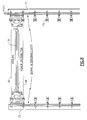
- a flexible film 32 (Figure 3a) has wiring on two surfaces on which are mounted memory array chips 34, their decoupling capacitors 36 and a terminating resistor chip 38. The film 32 is folded along the centre line 33 of its long axis, and mounted to the substrate with outer lead bonds 39 along the two long edges.
- a ground plane film 40 ( Figure 3b) is connected at one end 42 to edge 44 of the film 32 and provides a return path for the long address and control wires 46 which originate and terminate at the end to which the ground plane is attached.
- a compliant member 48 such as a spring or strip of elastomer, is placed between two rows of back-to-back films 32.
- a cooling hat 49 having cavities 50 is placed over this assembly so that the memory array chips 34 on the films 32 are pressed against the inside surfaces of the cavities 50 receiving the back-to-back films to provide good thermal conductivity.
- a thin layer of thermally conductive oil further enhances this interface.
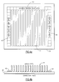
- FIG. 4 a In a typical layout of a memory ECM ( Figure 4 a ) employing this construction, film strips 32 fill the centre of the top surface of a module 20 in an array 41, and logic support chips are located around the same three sides of the perimeter carrying the signal I/O pads on the lower surface of the module 20 ( Figure 4 b ).
- the logic support chips include input support chips 42, address redrive chips 43 and output support chips 44.
- the data input and the data output support chips are at opposite edges of the module, so that address, input data and control signals enter at one edge and output data leaves from the opposite edge.
- Each ECM comprises a power boundary and so has its own dedicated power supply.
- the module 20 and its power supply 51 are assembled together to form a field replaceable unit (FRU) 50 ( Figure 5).
- the power supply 51 comprises a primary section 52, a secondary section 53 and a water cooling manifold 54, the latter having a generally arcuate outer edge 55 conforming to the outer surface of the computer system.
- the interface between the module 20 and its power supply 50 is via power planes 56 and power connecter 57.
- the power planes section 56 is an extension of the secondary section 53. Power pads (not shown) on the under surface of the power planes 56 correspond with power pads 23 on the mating surface of the module.
- connection between the power plane 56 and the module 20 is accomplished by use of an interposer connector 57, such as Shin-Etsu's Polymer MAF, Fujipoly's W series, TRW's "Fuzz-Button” or similar connectors by AMP Inc., Rogers Corp., AT&T and others.
- the connector 57 ( Figure 6) comprises a flat sheet of elastomer 61 embedded with metal fibres 62 to maintain paths of conductivity through the thickness of the elastomer. There is, however, no conductivity along either of the other dimensions of the elastomer.
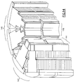
- FRUs ( Figure 5) are stacked like trays above each other ( Figure 7). Their signal interconnections are made with zero insertion force (ZIF) connectors.
- ZIF zero insertion force
- a suitable connector of this type is described in US -A- 4,636,019.
- An FRU 50 is inserted between two wiring boards 71 and 72 along connector guides 73 so that, when seated, the ZIF connectors make the electrical connection between the module and the boards.
- the third (front) board and its associated connector are omitted in this illustration to show an embodiment for an application where the front board is not required.
- Each stack may operate as a stand-alone unit 100 ( Figure 10) or may be combined with another stack to form a joined pair 102.
- the connections between adjacent stacks are made by flexible wiring 104, while the global wiring connections 106 are connected to individual ECMs 20 along their third edges carrying the I/O pads 26 ( Figure 2b).
- the joined pair 102 forms a important part of this invention.
- processors 110 In an example of the packaging concept of the present invention, sixty four processors 110 ( Figure 11), numbered 00 to 63 in four groups, and one hundred and twenty eight BSMs 112, numbered 00 to 127 in four groups, are split into four clusters, each cluster containing sixteen processors, thirty two BSMs and the associated request and respond switches 114, numbered 0 to 3.
- Each processor is assumed to comprise a scalar engine and two vector pipes, although from a packaging interconnection viewpoint, only the number of pipes on an ECM is important.
- two processors are mounted on an ECM, for a total of two scalars, four vector pipes and twelve logical ports per ECM.
- each logical port is duplicated to match the switch configuration.
- a vector pipe in processor number 00 has two double word fetch ports and one double word store port to switch 0, with a duplicate set of ports connected to switch 1.
- each BSM has one fetch and one store double word port to its local switch, with duplicates to a remote switch.
- the cross coupling is such that each processor has access to each BSM.
- the other side also having sixty four processors and one hundred and twenty eight BSMs with their corresponding request and respond switches, is the mirror image of side illustrated. Data transfer between the two sides is accomplished through an inter-side switch 116.
- the resulting computer system comprises one hundred and twenty eight processors and two hundred and fifty six BSMs in a massively parallel system.
- the request switch ECMs and the respond switch ECMs can be interchanged between stacks A and B.
- the interconnections between stacks A and B are by means of flexible, planar cables 122 and 124.
- the interconnections 126 between the processor ECMs and respond switch ECMs in stack A and the interconnections 128 between the BSM ECMs and request switch ECMs in stack B may be by means of flexible cable or rigid circuit boards.
- the arrows indicate the direction of data flow around the cluster.
- the natural flow of information through the memory modules M1 to M8 is uni-directional, data entering at the right of the ECMs M1 to M8 and leaving at the left. Similar uni-directional flow occurs in the request and respond switch modules and in the processor modules.
- the arrangement assumes that the total loop delay is an integral number of cycle times CK, meaning that if a clock pulse is inserted at sync point 131, it will propagate around in the loop in an integral number of processor cycle times. This may require in a specific implementation the insertion of a small delay in the loop circuit to account for a fractional cycle time in the total loop propagation time.
- the arrangement also assumes that parallel delays are equal. This means that a clock pulse inserted at sync point 131 will propagate through any of the processors 132 and arrive at sync point 133 at the same time.
- a clock pulse at sync point 133 will propagate through any of request switches 134 and arrive at sync point 135 at the same time, and a clock pulse at sync point 135 will propagate through any of BSMs 136 and arrive at sync point 137 at the same time.
- the arrangement assumes that there is at least one absolute sync point, for example, sync point 131.
- the arrangement just described reduces the packaging delay in the memory latency path by approximately one half over a package using a more conventional "card-on board” (COB) or "bookcase” design if the same packing density assumptions are made for each case and also reduces the effects of clocking skews and latency.
- COB card-on board
- bookcase design if the same packing density assumptions are made for each case and also reduces the effects of clocking skews and latency.
- the use of three edges for signal interconnections compared to one for COB or "bookcase” designs reduces the interconnect density for the same number of I/Os or, alternatively, increases the I/Os usable for the same interconnect density. This is an important advantage, because the demands for more hardware at higher performance are forcing designs from area array connections on modules to edge connections for high density packaging.
- a sixteen processor cluster only uses two of the ECM's wirable edges of the ECM.
- the two opposite edges are used for connections within the local cluster, exemplified by processors 00-15, switch 0 and BSMs 00-31 ( Figure 11).
- Interconnections to other clusters use the third edge of the ECM, shown as global wiring connections 106 ( Figure 10).
- a first joined pair 142 is stacked above a second joined pair 144 and a third joined pair 146 is stacked above a fourth joined pair 148, with the stacked joined pairs 146 and 148 immediately adjacent stacked joined pairs 142 and 144.
- arrows 152 represent the local connections within the 16-way clusters 142, 144, 146, and 148 and arrows 154 represent the global buses between clusters.
- the schematic system of Figure 11 corresponds with the schematic physical interconnection of Figure 15, which graphically illustrates the "mirrored" images of the vertically and horizontally stacked joined pairs.
- these "mirror images” do not require different ECMs. Rather, the ECMs of one joined pair are merely connected upside down from the other joined pair, thus greatly saving manufacturing and inventory costs in the manufacture of a computer.
- the regular structure of the interconnect buses permits a simple wiring scheme. This regular structure allows the cables to be replaced in most cases by a rigid/flex board structure, for example a "multi-wire board”, sometimes known as an "encapsulated circuit board” or ECB.
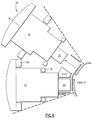
- the overall footprint of a 128-way system with 128 Gbytes of tightly coupled main memory is shown in Figure 16. It can be seen that the ECMs 20 containing the logic and memory are close together, with all the global wiring occurring on the inner arc and the massive utility functions (power supplies and cooling distribution) filling the much larger outer arc.
- the diameter of the footprint is approximately 10 feet (3.048 metres) based on a typical package design of system and technology assumptions including chip circuit and bit density, power distribution and cooling capability, power supply volumetric efficiency (including cooling) and interconnection densities at all levels.
- the packaging principles described, however, are virtually independent of technology capabilities, and the specific system illustrated may be varied over a wide range.
Landscapes
- Engineering & Computer Science (AREA)
- Theoretical Computer Science (AREA)
- General Engineering & Computer Science (AREA)
- Physics & Mathematics (AREA)
- General Physics & Mathematics (AREA)
- Computer Hardware Design (AREA)
- Power Engineering (AREA)
- Human Computer Interaction (AREA)
- Multi Processors (AREA)
Applications Claiming Priority (2)
| Application Number | Priority Date | Filing Date | Title |
|---|---|---|---|
| US67558391A | 1991-03-26 | 1991-03-26 | |
| US675583 | 1991-03-26 |
Publications (2)
| Publication Number | Publication Date |
|---|---|
| EP0506224A2 true EP0506224A2 (de) | 1992-09-30 |
| EP0506224A3 EP0506224A3 (en) | 1994-05-11 |
Family
ID=24711125
Family Applications (1)
| Application Number | Title | Priority Date | Filing Date |
|---|---|---|---|
| EP19920301131 Withdrawn EP0506224A3 (en) | 1991-03-26 | 1992-02-11 | Computer system package |
Country Status (2)
| Country | Link |
|---|---|
| US (1) | US5497471A (de) |
| EP (1) | EP0506224A3 (de) |
Cited By (1)
| Publication number | Priority date | Publication date | Assignee | Title |
|---|---|---|---|---|
| EP0734643A4 (de) * | 1994-09-20 | 1997-04-02 | Peter M Compton | Datenverarbeitungsvorrichtung |
Families Citing this family (3)
| Publication number | Priority date | Publication date | Assignee | Title |
|---|---|---|---|---|
| EP0905440A1 (de) * | 1997-09-26 | 1999-03-31 | James Arthur Phillips | Leuchtzeichen mit Kantenbeleuchung |
| US6109929A (en) * | 1998-07-29 | 2000-08-29 | Agilent Technologies, Inc. | High speed stackable memory system and device |
| US8214786B2 (en) * | 2004-09-08 | 2012-07-03 | Hewlett-Packard Development Company, L.P. | Scalable, component-accessible, and highly interconnected three-dimensional component arrangement within a system |
Family Cites Families (10)
| Publication number | Priority date | Publication date | Assignee | Title |
|---|---|---|---|---|
| US4237546A (en) * | 1979-01-31 | 1980-12-02 | Technology Marketing, Inc. | Multi-layered back plane for a computer system |
| GB2123216B (en) * | 1982-06-19 | 1985-12-18 | Ferranti Plc | Electrical circuit assemblies |
| WO1986004208A1 (fr) * | 1984-12-28 | 1986-07-17 | Micro Engineering Co., Ltd. | Procede d'empilage de cartes de circuits imprimes |
| US4868712A (en) * | 1987-02-04 | 1989-09-19 | Woodman John K | Three dimensional integrated circuit package |
| US5058053A (en) * | 1988-03-31 | 1991-10-15 | International Business Machines Corporation | High performance computer system with unidirectional information flow |
| EP0335482A2 (de) * | 1988-03-31 | 1989-10-04 | International Business Machines Corporation | Rechnersystem mit grosser Leistung |
| JP2591677B2 (ja) * | 1989-04-21 | 1997-03-19 | 株式会社 グラフィコ | 放射型・パラレル・システムバス |
| JP2626698B2 (ja) * | 1989-06-15 | 1997-07-02 | 株式会社 グラフィコ | 放射型・パラレル・システムバス |
| US5063475A (en) * | 1990-03-19 | 1991-11-05 | International Business Machines Corporation | Multileveled electronic assembly with cooling means |
| US5150279A (en) * | 1991-03-18 | 1992-09-22 | International Business Machines Corporation | High performance computer system with platters and unidirectional storage modules therebetween |
-
1992
- 1992-02-11 EP EP19920301131 patent/EP0506224A3/en not_active Withdrawn
-
1994
- 1994-11-14 US US08/339,512 patent/US5497471A/en not_active Expired - Fee Related
Cited By (1)
| Publication number | Priority date | Publication date | Assignee | Title |
|---|---|---|---|---|
| EP0734643A4 (de) * | 1994-09-20 | 1997-04-02 | Peter M Compton | Datenverarbeitungsvorrichtung |
Also Published As
| Publication number | Publication date |
|---|---|
| EP0506224A3 (en) | 1994-05-11 |
| US5497471A (en) | 1996-03-05 |
Similar Documents
| Publication | Publication Date | Title |
|---|---|---|
| US5150279A (en) | High performance computer system with platters and unidirectional storage modules therebetween | |
| US5317477A (en) | High density interconnection assembly | |
| US6853557B1 (en) | Multi-channel memory architecture | |
| US6574726B2 (en) | Modular architecture for high bandwidth computers | |
| US6469901B1 (en) | System and method for cartridge-based, geometry-variant scalable electronic systems | |
| US6202110B1 (en) | Memory cards with symmetrical pinout for back-to-back mounting in computer system | |
| US7072201B2 (en) | Memory module | |
| US8549092B2 (en) | Memory network methods, apparatus, and systems | |
| US5058053A (en) | High performance computer system with unidirectional information flow | |
| US5497471A (en) | High performance computer system which minimizes latency between many high performance processors and a large amount of shared memory | |
| US20020097563A1 (en) | Apparatus and method for scalable electronic systems using cascadable floor modules | |
| US7692929B2 (en) | Interface connection device for connecting a mainboard to a memory card having two series of memory modules | |
| US4763298A (en) | Memory assembly with cooling insert | |
| US20070224854A1 (en) | Memory module, method of manufacturing a memory module and computer system | |
| Shively et al. | A high performance reconfigurable parallel processing architecture | |
| EP0335482A2 (de) | Rechnersystem mit grosser Leistung | |
| WO2002027465A1 (en) | Apparatus and method for scalable interconnection networks in electronic systems | |
| JPH04113445A (ja) | 並列計算機 | |
| CN121900596A (zh) | 一种服务器系统结构 | |
| Louri et al. | Three-dimensional Optical Interconnects for High-density Chip-to-chip and Board-to-board Communications | |
| WO2002027437A2 (en) | Hexagonal structures for scalable electronic systems | |
| WO1993003442A1 (en) | Multiboard multiprocessor connector system | |
| WO2002028159A1 (en) | Apparatus, system, and method for hybrid-geometry resource cartridge-based, geometry-variant scalable electronic systems | |
| WO2002027880A1 (en) | Apparatus and method for scalable electronic systems using cascadable floor modules |
Legal Events
| Date | Code | Title | Description |
|---|---|---|---|
| PUAI | Public reference made under article 153(3) epc to a published international application that has entered the european phase |
Free format text: ORIGINAL CODE: 0009012 |
|
| AK | Designated contracting states |
Kind code of ref document: A2 Designated state(s): DE FR GB |
|
| 17P | Request for examination filed |
Effective date: 19930120 |
|
| PUAL | Search report despatched |
Free format text: ORIGINAL CODE: 0009013 |
|
| AK | Designated contracting states |
Kind code of ref document: A3 Designated state(s): DE FR GB |
|
| 18W | Application withdrawn |
Withdrawal date: 19960923 |