EP0507366A1 - LED-Belichtungskopf - Google Patents
LED-Belichtungskopf Download PDFInfo
- Publication number
- EP0507366A1 EP0507366A1 EP92200619A EP92200619A EP0507366A1 EP 0507366 A1 EP0507366 A1 EP 0507366A1 EP 92200619 A EP92200619 A EP 92200619A EP 92200619 A EP92200619 A EP 92200619A EP 0507366 A1 EP0507366 A1 EP 0507366A1
- Authority
- EP
- European Patent Office
- Prior art keywords
- led
- integrated circuit
- circuit chips
- dice
- base plate
- Prior art date
- Legal status (The legal status is an assumption and is not a legal conclusion. Google has not performed a legal analysis and makes no representation as to the accuracy of the status listed.)
- Granted
Links
Images



Classifications
-
- B—PERFORMING OPERATIONS; TRANSPORTING
- B41—PRINTING; LINING MACHINES; TYPEWRITERS; STAMPS
- B41J—TYPEWRITERS; SELECTIVE PRINTING MECHANISMS, i.e. MECHANISMS PRINTING OTHERWISE THAN FROM A FORME; CORRECTION OF TYPOGRAPHICAL ERRORS
- B41J2/00—Typewriters or selective printing mechanisms characterised by the printing or marking process for which they are designed
- B41J2/435—Typewriters or selective printing mechanisms characterised by the printing or marking process for which they are designed characterised by selective application of radiation to a printing material or impression-transfer material
- B41J2/447—Typewriters or selective printing mechanisms characterised by the printing or marking process for which they are designed characterised by selective application of radiation to a printing material or impression-transfer material using arrays of radiation sources
- B41J2/45—Typewriters or selective printing mechanisms characterised by the printing or marking process for which they are designed characterised by selective application of radiation to a printing material or impression-transfer material using arrays of radiation sources using light-emitting diode [LED] or laser arrays
- B41J2/451—Special optical means therefor, e.g. lenses, mirrors, focusing means
-
- G—PHYSICS
- G06—COMPUTING OR CALCULATING; COUNTING
- G06K—GRAPHICAL DATA READING; PRESENTATION OF DATA; RECORD CARRIERS; HANDLING RECORD CARRIERS
- G06K15/00—Arrangements for producing a permanent visual presentation of the output data, e.g. computer output printers
- G06K15/02—Arrangements for producing a permanent visual presentation of the output data, e.g. computer output printers using printers
- G06K15/12—Arrangements for producing a permanent visual presentation of the output data, e.g. computer output printers using printers by photographic printing, e.g. by laser printers
- G06K15/1238—Arrangements for producing a permanent visual presentation of the output data, e.g. computer output printers using printers by photographic printing, e.g. by laser printers simultaneously exposing more than one point
- G06K15/1242—Arrangements for producing a permanent visual presentation of the output data, e.g. computer output printers using printers by photographic printing, e.g. by laser printers simultaneously exposing more than one point on one main scanning line
- G06K15/1247—Arrangements for producing a permanent visual presentation of the output data, e.g. computer output printers using printers by photographic printing, e.g. by laser printers simultaneously exposing more than one point on one main scanning line using an array of light sources, e.g. a linear array
Definitions
- the present invention relates to a LED (light-emitting diode) exposure head for use in a recording device for linewise recording information on a moving light-sensitive support.
- LED exposure heads comprise an assembly in alignment of a plurality of sub-bases onto which are mounted a row of LED dice along the centre, a row of integrated circuit chips at either side of the LED dice and printed circuit boards outboard of such rows of integrated circuit chips for electrically connecting the integrated circuit chips to electrical connectors, and optical imaging means for focussing the image of the LED's onto the image plane of a photoconductor.
- the LED dice are electrically connected with the integrated circuit chips through so-called chip-to-chip bonds, and the integrated circuit chips are in the same way connected with the circuit boards.
- the sub-bases are fitted to a common base and offer the advantage that they may be completely electrically and optically tested after their assembly before they are mounted one by one on the common base.
- the sub-bases are usually in the form of metal tiles of a light metal which has been gold-plated in view of a good electrical conductivity and of preventing corrosion.
- the LED dice, the integrated circuit chips and the printed circuit boards are fitted to the sub-bases by adhesive bonding.
- One example of the described explosure head is disclosed in US-A 4,536,778.
- LED exposure heads Another type of LED exposure heads is known in which there are no sub-bases but instead the distinct electronic components are mounted on one large ceramic substrate with printed conductor leads, the wire-bonding occurring from the LED dice to tee substrate and from the substrate to the integrated circuit chips.
- This type of exposure head causes less problems with undesired reflections, but requires twice the number of bonding wires.
- the LED dice are directly wire-bonded to the integrated circuit chips. This technique is disclosed in JP-63 028 673.
- the causes for undesired light reflections in the first type of LED exposure heads are as follows.
- Self-focussing lenses for focussing the image of the LED's in the image plane of the photoconductor have become available with an increased depth of field.
- An increased depth of field leads to a better image quality but unfortunately also causes a better reproduction of undesirable light spots, such as reflections of the radiation beams of the LED's on surrounding parts of the structure.
- the thickness of the LED dice is still getting smaller since a smaller thickness means a shorter thermic path from the light-emitting surface to the rearside of the LED's whereby the heat-transfer for the active layer (i.e. the light-emitting layer) improves and the working temperature of said layer becomes lower.
- a lower temperature means more light since the temperature coefficient of a LED amounts to approximately - 0.7 %/°C.
- the electric series resistance is smaller as the thickness of the LED chips becomes smaller.
- the top surface with the bonding pads of the LED's will be located lower than the top surface with the corresponding bonding pads of the integrated circuit chips.
- the electric wire connections from the LED's to the integrated circuit chips are made by means of highly-reflective wires, such as gold wire in the case of thermocompression bonding, or aluminium wire in the case of ultrasonic bonding, it will be understood that as such wire, and more in particular the loop in its path from one pad to the other will run at a smaller angle than before with respect to a normal on the LED's, the greater will be the risk for such loop to intersect the light cone emitted by a LED and thus for undesirable reflection of light on the intersected portion of such loop.
- highly-reflective wires such as gold wire in the case of thermocompression bonding, or aluminium wire in the case of ultrasonic bonding
- a LED (light-emitting diode) exposure head for use in a recording device for linewise recording information on a moving light-sensitive support, said exposure head comprising at least one metal base plate onto which are mounted a row of LED dice along the centre, a row of integrated circuit chips on at least one side of the LED dice and a printed circuit board outside of such row of integrated circuit chips for electrically connecting the circuit boards to electric connectors, the thickness of the LED dice being smaller than that of the integrated circuit chips, and optical imaging means for focussing the image of the LED's in the image plane of the light-sensitive support, is characterized in that said base plate has a raised rib for mounting the LED dice at a height above the base plate which is such that their electric bonding pads are at a level higher than that of the corresponding bonding pads of the integrated circuit chips, and wherein the paths of the wire bonded electric connections are such that they are out of contact with the light cones emitted by the LED's.
- a LED exposure head with a provision that causes the underside of the LED dice to take a position that is higher than that of the base plate on which they are mounted is known from JP-A 63-28673.
- the base plate is a ceramic structure and the mentioned provision is an electrode that puts the undersides of the adjacent LED's in electrical contact.
- the LED's have a thickness that equals that of the integrated circuit chips.
- the raised rib according to the present invention is suitably located at the centre of the base plate and has a width nearly that of the LED dice and a height such that the top of the LED dice is clearly higher than the top of the integrated circuit chips. Since the thickness of the integrated circuit chips is larger than the thickness of the LED dice, it will be understood that the height of the mentioned rise will have to be larger than the difference in height between both components. Usual values of the height of the inventive raised ribs are between 0.2 and 1.0 mm but these values are not limitative for the present invention.
- the raised rib on the base is obtained by erosion-etching of a flat metal plate thereby to leave the original thickness at the centre and to reduce the thickness at the locations where the integrated circuit chips and/or the printed circuit boards will be mounted on the base.
- a LED exposure head may comprise only one base with a plurality of LED dice. It is clear that a head suitably comprises a plurality of LED bases in the form of sub-bases which are mounted on a common supporting base.
- light-sensitive support denotes in the present specification a photoconductor drum as known in the art of electrophotographic printers, but it encompasses also photoconductive and otherwise light-sensitive supports in sheet or belt from onto which an image may be formed via exposure by a LED exposure head.
- the arrow 10 illustrates generally the engine of a xerographic printer.
- engine denotes the parts of the apparatus that are involved in the production of the image.
- a printer comprises a plurality of other parts such as a paper supply, a toner supply, a fixing station, drive means for rotation of the drum and for the paper transport, a toner fixing station, an electronic control circuit, etc. These parts are known in the art and are irrelevant for the understanding of the further description of the present embodiment of the invention.
- the engine comprises a photoconductor drum 12 which may be an aluminium cylinder coated with a photosensitive photoconductor, and which is rotatable in the direction of the arrow 13.
- a photoconductor drum 12 which may be an aluminium cylinder coated with a photosensitive photoconductor, and which is rotatable in the direction of the arrow 13.
- Around the drum are provided the following stations in angularly spaced relationship.
- a corona-discharge station 14 which is used to uniformly electrostatically charge the surface of the drum 12.
- a colour developing unit 16 which is arranged for applying coloured toner to the line-wise discharge drum surface by means of a developer sleeve 17, also called a magnetic brush.
- a black-and-white developing unit 18. which is arranged for applying a black toner to the charge pattern on the drum by means of a developer sleeve 19.
- a corona transfer station 21 which applies a corona charge of a sign opposite to that of the toner to the underside of the paper to attract the toner from the drum onto the paper to form a visible, developed image.
- a paper separation station 23 which applies charges to the paper so that it can be easily separated from the drum.
- a paper separator 24 which functions to ensure that the paper sheet is reliably separated from the drum.
- This toner may be conveyed to a toner collecting bottle of the apparatus.
- a main erase 26 which has a lamp 27 for neutralising any residual charge remaining on the surface of the photoconductor drum after cleaning.
- the LED exposure head 15 receives a first image signal to produce on the photoconductor drum 12 a charge pattern that is developed by the black developing unit 18.
- the paper sheet that is removed by the separator 24 is passed through a toner fixing station which functions to melt the toner image into the paper sheet.
- the paper sheet is then returned by an appropriate conveying mechanism to the feed entry 20 for receiving a second toner image from the photoconductor drum, this time the colour image produced by the station 16 and by appropriate exposure by the head 15.
- An example of the use of the described two-colour development is that of a letter or advertising sheet, which bears a conventional black-and-white text, and the heading and/or the bottom of which bear(s) a coloured company logo.
- fig. 1 shows that the different stations around the photoconductor drum are located in closely spaced relationship. Both developing stations take quite an important part of the angular space around the photoconductor drum.
- the head 15 is mounted within a housing which is composed of a base 28 and a cover 29.
- the base may be an extrusion-moulded component of a light metal alloy, such as aluminium, with a plurality of cooling fins at the outside and four rectangular ribs, viz. two outer 50 and two inner ribs 51 (see fig. 2) at the inside, whereas the cover has an elongate opening in which lens means 30 in the form of a Selfoc is fitted for projecting the image of the LED's of the exposure head onto a line 31 on the surface of the drum 12.
- section A being a true plan view
- section B showing the base with the LED's omitted
- section C showing an end section of the head.
- Base 28 whose inside is turned upwardly, is provided with an elongate copper bar 32, which is fitted in the space between two inner ribs 51 of the base by means of a thermally conductive adhesive that allows minor dimensional changes of the base and of the bar, caused by the heating of these elements at operation of the exposure head.
- Two elongate printed circuit strips 34 and 35 are located on the base at either side of the bar 32.
- the thickness of the strips is slightly less than the distance over which the bar protrudes beyond the ribs 50 and 51.
- a plurality of LED modules 36 are die-bonded in closely spaced side by side relationship to the bar 28 by means of an electrically and thermally conductive adhesive, such as a silver-filled epoxy adhesive.
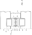
- Each LED module is in fact an assembly of the following components on a sub-base which is constituted by a tiny metal plate 38 (see fig. 3).
- each dice is about 8 mm long and about 1 mm wide.
- each plate On each side of the row of LED dice on each plate there is a row of integrated circuit chips 41 and 42 respectively, which are equally cemented in an electrically and thermally conductive way to the base plate.
- the chips can comprise the drivers for the LED's, a shift register, a latch register and occasional further control and test circuits.
- circuit boards in the form of a conventional thick film circuit on a ceramic base, such as 43 and 45 which are equally cemented to the base plate.
- the circuit boards are connected through electric connections such as 46 with the elongate printed circuit strips 34 and 35 at connection points such as 47.
- the two printed circuit strips 34 and 35 have end connectors such as 48 and 49 for bringing signals and power into the circuit.
- Wire-bonded electric connections are provided between the LED dice 39 and the corresponding output pads of the integrated circuit chips 41 and 42, and between the input pads of the chips and the corresponding thick film circuits 43 and 44.
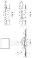
- the improvement in accordance with the invention relates to the connections between the LED dice and the adjacent integrated circuit chips. This is illustrated in detail in fig. 4, which shows a side view of one LED module 36.
- the module comprises a sub-base in the form of a metal plate or tile 38. which has a central raised rib 52.
- the described cross-sectional shape of the sub-base can be obtained in different ways, such as by die-casting, die-stamping, or milling of a plate.
- a very suitable technique for the production of the sub-base consists in erosion-etching a conventional flat strip of copper or the like in such a way that a central ridge of original thickness is left, but that the opposed sides are uniformly reduced in thickness to the desired amount.
- LED dice 39 are cemented in a row to the front face of the sub-base by means of an electrically conductive adhesive.
- Each die has near either longitudinal end of its front face a row of bonding pads 53, and 54 respectively, for the LED's.
- the pads have been illustrated in the figure by a short thick line on top of the LED but actually they lie in the plane of the front face of the dice.
- the mentioned pads are connected with corresponding bonding pads 55, 56 of the integrated circuit chips through two rows of wire-bonded electric connections 57 and 58. These connections are in the present example made by the ultrasonic bonding of an aluminium wire with a thickness of approximately 32 micrometer.
- the bonding was done from the pads of the integrated circuit chips towards the corresponding pads of the LED dice.
- the capillary bonding tool of the bonding device is targeted on a bonding pad 56 of an integrated circuit chip 42.
- the tool descends bringing the free end of the wire in contact with the bonding pad.
- Ultrasonic energy is applied to bond the wire end, or the ball previously formed on it as the case may be, to the bonding pad.
- the tool rises to the loop height position h , the clamps of the tool being open so that wire is free to feed out the end of the capillary tool.
- the term "loop height" means the distance the tip of the bonding tool rises above the first bond.
- the bonding tool Simultaneously with its rising, the bonding tool is displaced in the direction of the corresponding pad 54 of the LED dice 39, wire being further pulled out from the tool. Then the tool deforms the wire against the bonding pad and while ultrasonic energy is applied a wedge-shaped bond is produced. With the tool still on the bond, the clamps move backward. This pulls at the bond and the wire will break at the thinnest cross-section of the bond. The tool then rises off the LED dice, leaving the wedge bond.
- the wire loops thus formed have a configuration as shown by numerals 57 and 58.
- the loops comprise a first portion which runs upwardly, starting from the integrated circuit chips, and a second portion which slightly descends towards the LED dice. Since radiation of the LED's occurs according to a light cone with an opening angle Alpha, it is clear that there is a good clearance between a connection 58 and the adjacent boundary of the light cone as indicated by the line 59.
- loop heigh h1 is rather limited, in the present example 0.317 mm. This has the advantage of a good separation between the wire loops 57, 58 and the light cone 59, but the disadvantage that there is no sharp bending or kink in the connection, what can be the cause of occasional rupture of the bond on the integrated circuit chip under the influence of bending stresses in the connecting wire. Therefore, a preferred bond is one as illustrated in fig. 6, where h2 equals 0.508 mm.
- the increased loop height is the cause that a noticeable kink 60 is produced in the wire loops as the bonding tool is lowered after it has been positioned above the bonding pad 54. In this way, bending stresses in the wire are seriously reduced.
- the invention is not limited to the described embodiment.
- the LED dice may comprise two staggered rows of LED's in order to increase the printing resolution.
- the exposure head may comprise only one row of integrated circuit chips to drive the LED's, rather than two rows as shown.
- the sub-bases may be constructed in another way than by erosion-etching, such as by die-stamping, or milling as mentioned already.
- the mounting means for the LED dice can also be obtained by providing a flat base plate with a central rib-like support which is fitted thereto, e.g. by soldering or brazing.
- erosion-etching is a cheap method for manufacturing the sub-bases with good precision. Further, this technique allows the manufacturing of a plurality of sub-bases in a common supporting frame so that handling of these elements in view of the mounting of the electric components thereon, the application of the electrical bondings, etc. becomes easier.
Landscapes
- Physics & Mathematics (AREA)
- Optics & Photonics (AREA)
- Engineering & Computer Science (AREA)
- Health & Medical Sciences (AREA)
- General Health & Medical Sciences (AREA)
- Toxicology (AREA)
- General Engineering & Computer Science (AREA)
- General Physics & Mathematics (AREA)
- Theoretical Computer Science (AREA)
- Printers Or Recording Devices Using Electromagnetic And Radiation Means (AREA)
- Dot-Matrix Printers And Others (AREA)
Applications Claiming Priority (2)
| Application Number | Priority Date | Filing Date | Title |
|---|---|---|---|
| EP91200785 | 1991-04-04 | ||
| EP91200785 | 1991-04-04 |
Publications (2)
| Publication Number | Publication Date |
|---|---|
| EP0507366A1 true EP0507366A1 (de) | 1992-10-07 |
| EP0507366B1 EP0507366B1 (de) | 1996-07-03 |
Family
ID=8207594
Family Applications (1)
| Application Number | Title | Priority Date | Filing Date |
|---|---|---|---|
| EP92200619A Expired - Lifetime EP0507366B1 (de) | 1991-04-04 | 1992-03-03 | LED-Belichtungskopf |
Country Status (4)
| Country | Link |
|---|---|
| US (1) | US5285217A (de) |
| EP (1) | EP0507366B1 (de) |
| JP (1) | JP3222191B2 (de) |
| DE (1) | DE69211881T2 (de) |
Cited By (2)
| Publication number | Priority date | Publication date | Assignee | Title |
|---|---|---|---|---|
| US7180252B2 (en) | 1997-12-17 | 2007-02-20 | Color Kinetics Incorporated | Geometric panel lighting apparatus and methods |
| US7358929B2 (en) | 2001-09-17 | 2008-04-15 | Philips Solid-State Lighting Solutions, Inc. | Tile lighting methods and systems |
Families Citing this family (7)
| Publication number | Priority date | Publication date | Assignee | Title |
|---|---|---|---|---|
| US6806659B1 (en) | 1997-08-26 | 2004-10-19 | Color Kinetics, Incorporated | Multicolored LED lighting method and apparatus |
| US7186003B2 (en) | 1997-08-26 | 2007-03-06 | Color Kinetics Incorporated | Light-emitting diode based products |
| US7064498B2 (en) | 1997-08-26 | 2006-06-20 | Color Kinetics Incorporated | Light-emitting diode based products |
| US7352339B2 (en) | 1997-08-26 | 2008-04-01 | Philips Solid-State Lighting Solutions | Diffuse illumination systems and methods |
| US7543956B2 (en) | 2005-02-28 | 2009-06-09 | Philips Solid-State Lighting Solutions, Inc. | Configurations and methods for embedding electronics or light emitters in manufactured materials |
| US7479973B2 (en) * | 2005-12-23 | 2009-01-20 | Dell Products L.P. | Method and apparatus for producing an image |
| WO2008081846A1 (ja) * | 2006-12-26 | 2008-07-10 | Kyocera Corporation | 光プリンタヘッドおよびそれを備えた画像形成装置 |
Citations (2)
| Publication number | Priority date | Publication date | Assignee | Title |
|---|---|---|---|---|
| US4875057A (en) * | 1988-09-01 | 1989-10-17 | Eastman Kodak Company | Modular optical printhead for hard copy printers |
| WO1990002387A1 (en) * | 1988-08-30 | 1990-03-08 | Eastman Kodak Company | Light emitting diode printhead |
Family Cites Families (8)
| Publication number | Priority date | Publication date | Assignee | Title |
|---|---|---|---|---|
| JPS5881181A (ja) * | 1981-11-06 | 1983-05-16 | Matsushita Electric Ind Co Ltd | 感熱記録ヘツド |
| DE3276289D1 (en) * | 1982-02-19 | 1987-06-11 | Agfa Gevaert Nv | Recording apparatus |
| JPS61270176A (ja) * | 1985-05-24 | 1986-11-29 | Kyocera Corp | 光プリンタヘツド |
| JPH0671796B2 (ja) * | 1985-12-18 | 1994-09-14 | 三洋電機株式会社 | 光プリンタヘツド |
| JPS63216391A (ja) * | 1987-03-04 | 1988-09-08 | Nec Corp | Led記録ヘツド |
| US4907034A (en) * | 1987-03-06 | 1990-03-06 | Fuji Photo Film Co., Ltd. | Image recorder using recording head |
| US4829321A (en) * | 1987-04-23 | 1989-05-09 | Hitachi Cable, Ltd. | Optical printer head with a light emitting diode array |
| US4929965A (en) * | 1987-09-02 | 1990-05-29 | Alps Electric Co. | Optical writing head |
-
1992
- 1992-03-03 DE DE69211881T patent/DE69211881T2/de not_active Expired - Fee Related
- 1992-03-03 EP EP92200619A patent/EP0507366B1/de not_active Expired - Lifetime
- 1992-03-06 US US07/846,918 patent/US5285217A/en not_active Expired - Fee Related
- 1992-04-02 JP JP11080192A patent/JP3222191B2/ja not_active Expired - Fee Related
Patent Citations (2)
| Publication number | Priority date | Publication date | Assignee | Title |
|---|---|---|---|---|
| WO1990002387A1 (en) * | 1988-08-30 | 1990-03-08 | Eastman Kodak Company | Light emitting diode printhead |
| US4875057A (en) * | 1988-09-01 | 1989-10-17 | Eastman Kodak Company | Modular optical printhead for hard copy printers |
Non-Patent Citations (1)
| Title |
|---|
| PATENT ABSTRACTS OF JAPAN vol. 12, no. 236 (M-715)(3083) 6 July 1988 & JP-63 028 673 ( KYOCERA CORP ) 6 February 1988 * |
Cited By (2)
| Publication number | Priority date | Publication date | Assignee | Title |
|---|---|---|---|---|
| US7180252B2 (en) | 1997-12-17 | 2007-02-20 | Color Kinetics Incorporated | Geometric panel lighting apparatus and methods |
| US7358929B2 (en) | 2001-09-17 | 2008-04-15 | Philips Solid-State Lighting Solutions, Inc. | Tile lighting methods and systems |
Also Published As
| Publication number | Publication date |
|---|---|
| DE69211881D1 (de) | 1996-08-08 |
| US5285217A (en) | 1994-02-08 |
| JP3222191B2 (ja) | 2001-10-22 |
| EP0507366B1 (de) | 1996-07-03 |
| DE69211881T2 (de) | 1997-02-06 |
| JPH05201063A (ja) | 1993-08-10 |
Similar Documents
| Publication | Publication Date | Title |
|---|---|---|
| EP0460194B1 (de) | Leuchtdiodendruckkopf mit signalverteilungsgerät | |
| US4706130A (en) | Image recording apparatus utilizing light emitting diodes with pixel shape correction | |
| US5323084A (en) | Light emitting diode printhead | |
| US4536778A (en) | Recording apparatus with modular LED array of higher production yield | |
| US6559879B1 (en) | LED array head, circuit board, and LED array chip | |
| GB2247959A (en) | Optical writing heads | |
| EP0792750A2 (de) | Vorrichtung und Verfahren zur Aufzeichnung | |
| EP0507366B1 (de) | LED-Belichtungskopf | |
| US4827290A (en) | LED array head using a fiber bundle | |
| US5257049A (en) | LED exposure head with overlapping electric circuits | |
| JPH10211732A (ja) | ヘッド及びその実装方法 | |
| US5828400A (en) | Method for constructing a light-emitting diode printhead with a multiple DPI resolution driver IC | |
| JPH07314771A (ja) | Led書込装置 | |
| US5079567A (en) | Leaf-spring assembly for LED printhead | |
| US4921316A (en) | Integral fiber optic printhead | |
| JPH0721329Y2 (ja) | Ledアレ−ヘツド | |
| EP0510274A1 (de) | Leuchtdiodendruckkopf | |
| JP2524507B2 (ja) | 光書込みヘッド | |
| US5874984A (en) | Optical character generator for an electrographic printer | |
| JPH02212167A (ja) | Ledプリントヘッド | |
| GB2226185A (en) | A light emitting apparatus | |
| JPH08156320A (ja) | Ledプリンタヘッド及びその製造方法 | |
| JPH07178961A (ja) | 画像装置 | |
| JPH02122955A (ja) | 光プリンタヘッド | |
| JPH08148723A (ja) | 光プリントヘッド及びその製造方法 |
Legal Events
| Date | Code | Title | Description |
|---|---|---|---|
| PUAI | Public reference made under article 153(3) epc to a published international application that has entered the european phase |
Free format text: ORIGINAL CODE: 0009012 |
|
| AK | Designated contracting states |
Kind code of ref document: A1 Designated state(s): BE DE FR GB |
|
| 17P | Request for examination filed |
Effective date: 19930204 |
|
| GRAH | Despatch of communication of intention to grant a patent |
Free format text: ORIGINAL CODE: EPIDOS IGRA |
|
| 17Q | First examination report despatched |
Effective date: 19951130 |
|
| GRAA | (expected) grant |
Free format text: ORIGINAL CODE: 0009210 |
|
| AK | Designated contracting states |
Kind code of ref document: B1 Designated state(s): BE DE FR GB |
|
| REF | Corresponds to: |
Ref document number: 69211881 Country of ref document: DE Date of ref document: 19960808 |
|
| GRAH | Despatch of communication of intention to grant a patent |
Free format text: ORIGINAL CODE: EPIDOS IGRA |
|
| ET | Fr: translation filed | ||
| PLBE | No opposition filed within time limit |
Free format text: ORIGINAL CODE: 0009261 |
|
| STAA | Information on the status of an ep patent application or granted ep patent |
Free format text: STATUS: NO OPPOSITION FILED WITHIN TIME LIMIT |
|
| REG | Reference to a national code |
Ref country code: GB Ref legal event code: 746 Effective date: 19970418 |
|
| 26N | No opposition filed | ||
| REG | Reference to a national code |
Ref country code: FR Ref legal event code: D6 |
|
| PGFP | Annual fee paid to national office [announced via postgrant information from national office to epo] |
Ref country code: FR Payment date: 20000223 Year of fee payment: 9 |
|
| PGFP | Annual fee paid to national office [announced via postgrant information from national office to epo] |
Ref country code: GB Payment date: 20000313 Year of fee payment: 9 |
|
| PGFP | Annual fee paid to national office [announced via postgrant information from national office to epo] |
Ref country code: BE Payment date: 20010226 Year of fee payment: 10 |
|
| PG25 | Lapsed in a contracting state [announced via postgrant information from national office to epo] |
Ref country code: GB Free format text: LAPSE BECAUSE OF NON-PAYMENT OF DUE FEES Effective date: 20010303 |
|
| GBPC | Gb: european patent ceased through non-payment of renewal fee |
Effective date: 20010303 |
|
| PG25 | Lapsed in a contracting state [announced via postgrant information from national office to epo] |
Ref country code: FR Free format text: LAPSE BECAUSE OF NON-PAYMENT OF DUE FEES Effective date: 20011130 |
|
| REG | Reference to a national code |
Ref country code: FR Ref legal event code: ST |
|
| PG25 | Lapsed in a contracting state [announced via postgrant information from national office to epo] |
Ref country code: BE Free format text: LAPSE BECAUSE OF NON-PAYMENT OF DUE FEES Effective date: 20020331 |
|
| BERE | Be: lapsed |
Owner name: *AGFA-GEVAERT N.V. Effective date: 20020331 |
|
| PGFP | Annual fee paid to national office [announced via postgrant information from national office to epo] |
Ref country code: DE Payment date: 20030214 Year of fee payment: 12 |
|
| PG25 | Lapsed in a contracting state [announced via postgrant information from national office to epo] |
Ref country code: DE Free format text: LAPSE BECAUSE OF NON-PAYMENT OF DUE FEES Effective date: 20041001 |