EP0507560A2 - Machines d'usinages par électro-érosion - Google Patents
Machines d'usinages par électro-érosion Download PDFInfo
- Publication number
- EP0507560A2 EP0507560A2 EP92302849A EP92302849A EP0507560A2 EP 0507560 A2 EP0507560 A2 EP 0507560A2 EP 92302849 A EP92302849 A EP 92302849A EP 92302849 A EP92302849 A EP 92302849A EP 0507560 A2 EP0507560 A2 EP 0507560A2
- Authority
- EP
- European Patent Office
- Prior art keywords
- signal
- machining
- current
- discharge
- controlling
- Prior art date
- Legal status (The legal status is an assumption and is not a legal conclusion. Google has not performed a legal analysis and makes no representation as to the accuracy of the status listed.)
- Granted
Links
Images







Classifications
-
- B—PERFORMING OPERATIONS; TRANSPORTING
- B23—MACHINE TOOLS; METAL-WORKING NOT OTHERWISE PROVIDED FOR
- B23H—WORKING OF METAL BY THE ACTION OF A HIGH CONCENTRATION OF ELECTRIC CURRENT ON A WORKPIECE USING AN ELECTRODE WHICH TAKES THE PLACE OF A TOOL; SUCH WORKING COMBINED WITH OTHER FORMS OF WORKING OF METAL
- B23H7/00—Processes or apparatus applicable to both electrical discharge machining and electrochemical machining
- B23H7/14—Electric circuits specially adapted therefor, e.g. power supply
- B23H7/16—Electric circuits specially adapted therefor, e.g. power supply for preventing short circuits or other abnormal discharges by altering machining parameters using adaptive control
-
- B—PERFORMING OPERATIONS; TRANSPORTING
- B23—MACHINE TOOLS; METAL-WORKING NOT OTHERWISE PROVIDED FOR
- B23H—WORKING OF METAL BY THE ACTION OF A HIGH CONCENTRATION OF ELECTRIC CURRENT ON A WORKPIECE USING AN ELECTRODE WHICH TAKES THE PLACE OF A TOOL; SUCH WORKING COMBINED WITH OTHER FORMS OF WORKING OF METAL
- B23H7/00—Processes or apparatus applicable to both electrical discharge machining and electrochemical machining
- B23H7/14—Electric circuits specially adapted therefor, e.g. power supply
- B23H7/20—Electric circuits specially adapted therefor, e.g. power supply for program control, e.g. adaptive
Definitions
- This invention relates to electric discharge machines, in particular it relates to an adaptive control method and apparatus for controlling the machining current in an electric discharge machine. More specifically, the present invention relates to an adaptive control method and apparatus for specifying the waveform of discharge current accurately and controlling the machining current pulse by setting the OFF time of a pulse even when the setting of the peak current value of the discharge current is changed.
- electric discharge machining may be performed with cumulative electric discharge craters formed by inducing pulses of discharge current at a high frequency.
- An electrode is positioned in an opposing relationship to a workpiece to be machined across a gap of microns for example via a machining liquid such as kerosene or water.
- This pulsed discharge current has nearly constant peak value and a pulse width repeating ON state and OFF state under the predetermined machining condition.
- the pulsed discharge current must be optimised in accordance with material, hardness of the workpiece and discharging state at the machining gap, for example.
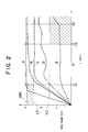
- the discharge current waveform across the gap formed between the electrode and the workpiece varies according to the state in the gap as shown in Figure 2.
- the machining liquid is decomposed into gas, tar and carbon and the decomposition products or metal sludges begin to intervene across the gap
- concentrated discharging during the electric discharge machining reduces the impedance across the gap and leads to the first discharge waveform having a fairly sharp rising edge and subsequent constant voltage level.
- the insufficient recovery of dielectric across the gap after a discharge current pulse may induce concentrated discharging and constant arc discharge which tends to damage machining electrodes and workpieces.
- the machining rate is reduced due to constant arc discharge.
- Concentrated discharging when less products lie across the gap leads to the second discharge waveform having a relatively favourable rising edge not involved in the area shown by a slanting line.
- a discharge waveform between LZ level for detecting low impedance and HZ level for detecting high impedance during discharging time indicates a stable dischargingstate, as the third and fourth waveforms shown. Further, when discharging is made via an impurity of high impedance, the fifth discharge waveform does not reach the HZ level.
- the OFF time of the pulse may preferably be shortened.
- the first to fifth discharge waveforms correspond to waveform A-E into Figure 2 which are described later, although the voltage levels of discharge current may be different from that in Figure 2.
- the HZ level, the LZ level and the ARC level in Figure 2 are detecting levels for specifying the waveform of discharge current.
- JP-B 47-50276 an electric machining apparatus has been disclosed in JP-B 47-50276.
- the detector detects a change of a gap voltage only during discharging time.
- this detector comprises a resistor connected in series with a machining electrode and a workpiece for sensing that start of spark discharging, a transistor which responds to the start of spark discharging and a resistor connected in parallel with a gap to detect a gap voltage at a certain portion of each discharge pulse.
- this detector comprises a resistor connected in series with a machining electrode and a workpiece for sensing the start of spark discharging, two transistors which responds to the start of spark discharging and two resistors connected in parallel with a gap and parallel to each other to detect a gap voltage at a certain two portions of each discharge pulse.
- JP-A 47-13795 and JP-A 51-119597 Other examples of the conventional controller are those shown in JP-A 47-13795 and JP-A 51-119597.
- the former is designed to detect a voltage variation slope, a mean voltage level and a high frequency component as a detected signal according to a gap voltage, only during discharging time and to extract more than two detected signals out of three.
- the extracted detected signals are used to display the machining state or used as a control signal for controlling the pulse generator or a servo device.
- the latter discloses a control method in which the discharge pulses repeated across the machining gap are detected to decide the machining state based on multiple groups of the discharge pulses and to produce a control signal digitally.
- a gap control device which comprises a discriminator for discriminating discharge pulses repeated across the machining gap, a counter for counting the discriminated results and a control signal generator for generating a gap control signal to increase or decrease the gap distance when the count equals the reference value.
- the detection level When the discharge current is controlled by measuring the total discharge current, the detection level must be changed according to the selected peak value.
- An object of the present invention is to provide an adaptive control method and apparatus for specifying the waveform of a discharge current accurately and controlling the machining current by suitably setting the OFF time of a pulse even when the setting of the peak current value of the discharge current is changed.
- an adaptive control apparatus for controlling the machining current pulse in an electric discharge machine comprises a first circuit for supplying said machining current pulse to the gap between a machining electrode and a workpiece, a second circuit for indirectly monitoring discharge current, area changing means for changing the detecting area according to a plurality of machining conditions, discriminating means for discriminating the waveform of the discharge current which is indirectly monitored by said second circuit and current controlling means for controlling the OFF time of said machining current pulse according to the discriminating results.
- the discriminating means decide whether a high impedance state exists or not at 5 microseconds after the start of spark discharging, whether a low impedance state exists or not at 15 microseconds after the start of spark discharging and whether an arc discharge state exists or not at the half time of discharge current pulse.
- an adaptive control method for controlling machining current pulse in an electric discharge machine comprises, a first step of setting machining condition, a second step of setting a detecting area according to machining condition, a third step of discriminating the waveform of the discharge current indirectly monitored and a fourth step of controlling the OFF time of the machining current pulse according to the discriminating results.
- the reference numeral "1" indicates a machining electrode for electric discharge machining.
- the electrode 1 is mounted in opposed relation to a workpiece 2 through the gap G of specified distance.
- a first circuit is provided.
- the first circuit comprises a first power source 3, current limiting resistors 4a, 4b and 4c, switching transistors 5a, 5b and 5c, and the gap G formed between the electrode 1 and the workpiece 2.
- the electrode 1 and the workpiece 2 are connected in series through the first power source 3.
- the current limiting resistors 4a, 4b and 4c giving a different current value are connected in parallel between the electrode 1 and the first power source 3.
- the switching transistors 5a, 5b and 5c are connected in parallel to each other between the respective resistor 4a, 4b and 4c and the electrode 1.
- Gap voltage sensor circuitry 6 is connected in parallel with the series circuit of the electrode 1, the workpiece 2 and the first power source 3.
- the gap voltage sensor circuitry 6 consists of the resistors 6a and 6b which branch a gap voltage.
- a second circuit connected in parallel with the gap voltage sensor circuitry 6 is provided.
- the second circuit comprises a second DC power source 9, current limiting resistor 7a, fourth switching transistor 8, detecting resistor 7b, and the gap G.
- the second DC power source 9 is connected between the limiting resistor 7a and the workpiece 2.
- Base voltage and emitter output of NPN type transistor 8 are supplied to the detecting circuit 10 for producing various signals.
- the detecting circuit 10 receives ON command data DN, OFF command data DF, gap voltage VG branched by the resistance 6a and 6b of said gap voltage sensor circuitry 6 and the clock signal S1.
- a detecting circuit 10 generates a signal S2 and a spark signal S3 which are supplied to the clock controller 20 together with the data DS.
- the clock controller 20 generates the ON clock signal S4 and the OFF clock signal S5 based on the signal S1, the signal S2 and the spark signal S3.
- the ON/OFF controller 30 receives the signal S4 and the signal S5.
- the base signal SB which is one of the control outputs of the ON/OFF controller 30, is supplied to the base of the fourth transistor 8 causing the transistor 8 to turn ON. Also, the base signal SB is supplied to the peak current controller 40.
- the output of the peak current controller is supplied to the respective base of the switching transistor 5a, 5b and 5c whereby the various peak values of discharge current are selected in this embodiment.
- the peak current data DIP is supplied to the peak current controller 40 and the detecting circuit 10.
- the ON/OFF controller 30 generates and supplies ON half signal S6, the ON end signal S8 and the OFF end signal S7 to the detecting circuit 10. Additionally, the base signal SB and the OFF end signal S7 is supplied to the clock controller 20.
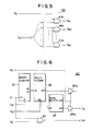
- the ON/OFF controller 30 consists of data selector 31 which selects and processes two major data of the ON command data DN and the OFF command data DF in response to a select signal described later, shifter 32 which shifts the value of the ON command data DN to half, three state buffers 33a and 33b which output the ON clock signal S4 and the OFF clock signal S5 selectively in response to the base signal SB, counter 34 which counts the selected signal S4 or signal S5, comparator 35a which generates a signal S9 to reset the counter 34 when the count B of the counter 34 equals to the value A of the output data of the data selector 31, comparator 35b which generates an output signal S6 when the count B of the counter 34 equals the value A of the output data of the shifter 32, toggle flip-flop 36 which receives the signal S9 from the comparator 35b at its input, invertor 37 which inverts the output signal of the flip-flop 36 to produce a falling edge from its rising edge, latch circuit 38a and 38b which latch into the rising edge of the flip
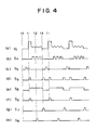
- This timing chart illustrates an example of a time relationship between a gap voltage VG, the ON clock signal S4, the OFF clock signal S5, signal S9, the base signal SB, the OFF end signal S7, the ON end signal S8 and the signal S6 when the value of the ON command data DN is 4 and the value of the OFF command data DF is 2.
- the trace (a) illustrates a gap voltage VG sensed by the gap voltage sensor circuitry 6.
- Traces (b) and (c) illustrate waveforms on the ON clock signal S4 and the OFF clock signal S5 which are supplied to the three state buffer 33a and 33b, respectively.
- the trace (d) illustrates the output signal S9 of the comparator 35a which is supplied to the flip-flop 36 and the counter 34.
- the trace (e) illustrates the base signal SB as the output signal of the flip-flop 36 which is supplied to the data selector 31 and the buffer 33a and 33b and also supplied to the peak current controller 40 and the transistor 8.
- the traces (f) and (g) illustrate waveforms of the OFF end signal S7 and the ON end signal S8 from the logic element 39a and 39b, respectively.
- the trace (h) illustrates the output signal S6 of the comparator 35b.
- the data selector 31 selects the OFF command data at time t0.
- the comparator 35a At time t1 when the counter 34 counts two OFF clock signals, the comparator 35a generates output signal S9 to cause the base signal SB to turn "on".
- the data selector 31 selects the ON command data in response to the base signal SB of "on" as select signal.
- the comparator 35b At time t2 when the count of the counter 34 equals to the value of output data of the shifter 32, the comparator 35b generates output signal S6.
- the comparator 35a At time t3 when the counter 34 counts four ON clock signals, the comparator 35a generates output signals S9 to cause the base signal SB to turn "off”. Then, time t1 to t3 are repeated.
- FIG. 5 shows the configuration of the peak current controller 40.
- This peak current controller 40 consists of AND circuit 41a to 41n which supplies output signals SBI, SB2 and SB3 to the bases of the transistors 5a, 5b and 5c, respectively, when receiving both of the base signal SB and the signal based on peak current data DIP. Since three transistors are provided in Figure 1 the AND circuit 41n is the AND current 41c which supplies output signal SB3.
- the clock controller 20 consists of a binary counter 21 which is reset when receiving the clock signal S1 and the base signal of "on”, multiplexer 22 which selects the output data from the binary counter 21 according to the data DS, rate multiplexer 23 which divides output signal from the multiplexer 22 to ten, three state buffers 24a and 24b which are selectively operable to supply the OFF clock signal S5 to the ON/OFF controller 30 according to the signal S2, and AND circuit 25 which supplies the ON clock signal S4 to the ON/OFF controller 30 when receiving both the clock signal S1 and the spark signal S3.
- the operation of the clock controller 20 is shown in the timing chart of Figure 7.
- This timing chart illustrates an example of time relationship between a gap voltage VG, the base signal SB, the clock signal S1, the spark signal S3, the signal S2, the ON clock signal S4 and the OFF clock signal S5.
- the trace (a) illustrates the gap voltage between the machining electrode 1 and the workpiece 2.
- the trace (c) illustrates the clock signal S1.
- the traces (d) and (e) illustrates the spark signal S3 indicative of the start of spark discharging and the signal S2 generated in the detecting circuit 10, respectively.
- the ON clock signal S4 illustrated in trace (f) is the clock signal S1 which generates only when the spark signal S3 is "on".
- the OFF clock signal S5 illustrated in trace (g) is the clock signal of the frequency calculated according to the data DS and the signal S2 which generates only when the base signal SB is "off”.
- the detecting circuit 10 consists of the discharge detector 11, the check clock generator 12 and the counter 13.
- the discharge detector 11 for detecting the discharging state across the gap G receives the peak current data DIP, the signal IS, the gap voltage VG, the base signal SB, the ON end signal S8, the OFF end signal S7, the signal S6 and the clock signal S1 as well as the signal t5 and t15 from the check clock generator 12.
- the signal IS indicates the current flowing at the point IS.
- the check clock generator 12 supplies the signal t5 and the signal t15 to the discharge detector 11 according to the spark signal S3 from the discharge detector 11 and the clock signal S1.
- the signal t5 represents elapse of 5 microseconds after the start of spark discharging and the signal t15 represents elapse 15 microseconds after the start of spark discharging.
- the counter 13 counts up or counts down responding to the signal SCU and the signal SCD from the discharge detector 11, respectively. Further, the clock controller 20 receives the signal S2 and the spark signal S3 from the discharge detector 11 and the data DS from the counter 13.
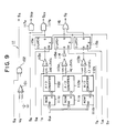
- the comparator 101 supplies the significant output signal level, eg level "1" when the gap voltage VG is lower than the reference voltage.
- the AND circuit 102 generates the spark signal S3 when receiving both the output signal of "1" from the comparator 101 and the base signal SB.
- ROMs 111a, 111b and 111c provide the data indicative of voltage value corresponding to the peak current data DIP.
- A/D converters 112a, 112b and 112c provide the HZ level signal indicative of high impedance, the LZ level signal indicative of low impedance and the ARC level signal based on the data from the ROMs 111a, 111b and 111c, respectively.
- the comparator 113a generates "1" when the HZ signal level is lower than the voltage level of the signal IS while the comparator 113b generates “1” when the LZ signal level is lower than the voltage level of the signal IS.
- the comparator 113c generates "1” when the ARC signal level is lower than the voltage level of the signal IS.
- the converter 114 converts output signal of the comparator 113a.
- the D-latch circuit 115a latches into output signal of the converter 114 with the signal t5 and is reset by the OFF and signal S7.
- the D-latch circuit 115b latches into output signal of the comparator 113b with the signal t15 and is reset by the OFF and signal S7.
- the D-latch circuit 115c latches into output signal of the comparator 113c with the signal S6 is reset by the OFF end signal S7.
- OR circuit 116 makes the logical sum of output from the D-latch circuit 115a and the D-latch circuit 115b to generate the signal S2.
- the AND circuit 117a generates the signal SCD when receiving both of output of the D-latch circuit 115c and the ON end signal S8, while the AND circuit 117b generates the signal SCU when receiving both of the inverted output of the D-latch circuit 115c and the ON end signal S8.
- the timing chart illustrates an example of time relationship between a gap voltage VG (a), the voltage level (b) of the signal IS, the signal T5 (c), the signal T15 (d), the base signal SB (e), the ON end signal S8 (f), the OFF end signal S7 (g), the signal S6 (h), the spark signal S3 (i), the signal SCD (j), the signal SCU (k) and the signal S2 (l).
- the voltage level of the signal IS is illustrated in respect to the HZ level, the LZ level and the ARC level.
- the discharge detector 11 generates the signals illustrated in trace (i) to (l) on the basis of the operation of logic elements shown in Figure 9.
- levels for detecting the machining state such as HZ level, LZ level and ARC level which corresponds to peak current data DIP is shown in the table of Figure 11. All levels are based on the experimental results. As peak current on the left of the table increases, the voltage value at respective level are selected in reverse proportion as illustrated.
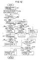
- Adaptive control apparatus and a method for controlling discharge current in electric discharge machines is described referring to the flow chart shown in Figure 12.
- the adaptive controller starts the processing operation and machining conditions including peak current are entered at step ST1.
- detecting voltage levels are set shown in Figure 11, as an example, according to peak current data DIP.
- step ST3 it is decided whether electric discharging has taken place at the gap G between the electrode 1 and the workpiece 2. The steps are looped until the electric discharging takes place. If it is decided that the electric discharging has taken place, processing stops for 5 microseconds at step ST4. Then at step ST5, it is decided whether the voltage level of the signal IS is higher than the LZ level or not. If yes, the signal S2 is generated at step ST6. Then, at step ST7, processing stops for 15 microseconds. If the voltage level of the signal IS is lower than the LZ level, step ST6 is skipped to step ST7 and processing stops for 15 microseconds.
- step ST8 it is decided whether the voltage level of the signal IS is lower than the HZ level or not. If yes, the process proceeds to next step ST9 and the signal S2 is generated. If the voltage level of the signal IS is higher than the HZ level at step ST8 or when the signal S2 is generated at step ST9, the process proceeds to next step ST17.
- step ST12 it is decided whether the voltage level of the signal IS is higher than the ARC level or not. If yes, the count up signal SCU is generated at next step ST13. If the voltage level of the signal IS is lower than the ARC level at step ST12, the count down signal SCD is generated at next step ST14. When the signal SCU is generated at step ST13, "n" is counted up by one at the next step ST15. When the signal SCD is generated at step ST13, "n” is counted down by one at the next step ST16. Following respective processing at steps ST8, ST9, ST15 and ST16, the process proceeds to step ST17.
- Figure 13 to 15 illustrate the performance of the above described embodiment compared to that of previously available technology.
- Figure 13 indicates a machining rate in electric discharge machining under the machining condition shown below.
- Figures 14 and 15 shown the surface condition of a workpiece with the conventional adaptive controller and the adaptive controller of the above embodiment.
- the machining condition is selected to have an ON time of 80 microseconds, OFF time of 20 microseconds, the peak current data DIP of 4 ampere (A) and the machining voltage applied to the gap of 90 volts (V). Further, the positive polarity is selected on the side of machining electrode (so-called "reverse polarity").
- the workpiece is made of rigor, while the tubular machining electrode has a diameter of 5 mm and is made of copper tungsten alloy (CuW) to cut ten 0.5 mm deep holes in a line under the above condition which is apt to induce the unstable discharging state.
- CuW copper tungsten alloy
- the conventional controller takes nearly double the time in any cut out of 10, while exhibiting arc craters, scars and stains at the bottom of cut holes due to unstable machining state.
- the controller of the present invention reduces conventional machining rate down by about half with little arc craters, scars and stains on the surface of the workpiece indicating excellent performance.
Landscapes
- Engineering & Computer Science (AREA)
- Chemical & Material Sciences (AREA)
- Chemical Kinetics & Catalysis (AREA)
- Electrochemistry (AREA)
- Mechanical Engineering (AREA)
- Automation & Control Theory (AREA)
- Electrical Discharge Machining, Electrochemical Machining, And Combined Machining (AREA)
Applications Claiming Priority (2)
| Application Number | Priority Date | Filing Date | Title |
|---|---|---|---|
| JP94715/91 | 1991-04-01 | ||
| JP3094715A JP3014793B2 (ja) | 1991-04-01 | 1991-04-01 | 加工電流制御方法及び加工電流制御装置 |
Publications (3)
| Publication Number | Publication Date |
|---|---|
| EP0507560A2 true EP0507560A2 (fr) | 1992-10-07 |
| EP0507560A3 EP0507560A3 (fr) | 1992-10-28 |
| EP0507560B1 EP0507560B1 (fr) | 1995-08-30 |
Family
ID=14117838
Family Applications (1)
| Application Number | Title | Priority Date | Filing Date |
|---|---|---|---|
| EP92302849A Expired - Lifetime EP0507560B1 (fr) | 1991-04-01 | 1992-03-31 | Machines d'usinages par électro-érosion |
Country Status (5)
| Country | Link |
|---|---|
| US (1) | US5352859A (fr) |
| EP (1) | EP0507560B1 (fr) |
| JP (1) | JP3014793B2 (fr) |
| DE (1) | DE69204338T2 (fr) |
| HK (1) | HK170295A (fr) |
Cited By (1)
| Publication number | Priority date | Publication date | Assignee | Title |
|---|---|---|---|---|
| US5345053A (en) * | 1992-08-25 | 1994-09-06 | Sodick Co., Ltd. | Method and apparatus for supplying power for electric discharge machining |
Families Citing this family (16)
| Publication number | Priority date | Publication date | Assignee | Title |
|---|---|---|---|---|
| US5539178A (en) * | 1992-11-18 | 1996-07-23 | Mitsubishi Denki Kabushiki Kaisha | Method and apparatus for controlling the power supply for electrical discharge machine |
| JP2914102B2 (ja) * | 1993-06-30 | 1999-06-28 | 三菱電機株式会社 | 放電加工機 |
| US5684417A (en) * | 1995-11-14 | 1997-11-04 | United Microelectronics Corporation | Data sensing apparatus of a read only memory device |
| JP3930962B2 (ja) * | 1998-02-03 | 2007-06-13 | 株式会社ソディック | 放電加工用電源装置における障害検知方法、放電加工用電源装置の制御方法及び放電加工用電源装置 |
| JP3830655B2 (ja) * | 1998-03-27 | 2006-10-04 | 株式会社ソディック | 放電加工装置用スイッチング回路の保護回路 |
| US6169261B1 (en) * | 1998-06-12 | 2001-01-02 | Industrial Technology Research Institute | Apparatus and method for generating an electric discharge for use in the line cutting of a workpiece |
| US7041933B2 (en) * | 2003-04-14 | 2006-05-09 | Meyer Tool, Inc. | Complex hole shaping |
| JP3950844B2 (ja) * | 2003-12-01 | 2007-08-01 | ファナック株式会社 | 放電加工機 |
| DE602006006457D1 (de) * | 2006-11-06 | 2009-06-04 | Agie Sa | Verfahren und Vorrichtung zum Funkenerosionsbearbeiten |
| JP4702961B2 (ja) * | 2007-08-07 | 2011-06-15 | 株式会社ソディック | 形彫放電加工方法および形彫放電加工装置 |
| TWI500466B (zh) * | 2012-09-25 | 2015-09-21 | Ind Tech Res Inst | 調變式放電加工控制裝置與方法 |
| US9452483B2 (en) * | 2012-11-14 | 2016-09-27 | General Electric Company | Electric discharge machining die sinking device and related method of operation |
| WO2014117226A1 (fr) * | 2013-02-04 | 2014-08-07 | Anca Pty Ltd | Contrôle d'impulsion et de jeu pour équipement d'usinage à décharge électrique |
| JP5800923B2 (ja) * | 2014-01-15 | 2015-10-28 | ファナック株式会社 | ワイヤ放電加工機の加工用電源装置 |
| JP6517847B2 (ja) * | 2017-01-18 | 2019-05-22 | ファナック株式会社 | ワイヤ放電加工機および加工方法 |
| CN113579377B (zh) * | 2021-06-11 | 2022-05-17 | 淮阴工学院 | 一种台阶式叶片双回路套料电解加工装置及方法 |
Family Cites Families (14)
| Publication number | Priority date | Publication date | Assignee | Title |
|---|---|---|---|---|
| US3729610A (en) * | 1969-02-07 | 1973-04-24 | I Kondo | Electrical discharge machining device using logical control |
| US3997753A (en) * | 1969-03-17 | 1976-12-14 | Inoue K | Control system and method for electric discharge machining (EDM) using a predetermined portion of each discharge pulse for monitoring |
| US3705286A (en) * | 1971-01-21 | 1972-12-05 | Iwao Kondo | Electric discharge machining device |
| JPS51119597A (en) * | 1975-04-14 | 1976-10-20 | Inoue Japax Res Inc | Method and apparatus of controlling gap in discharge processing |
| JPS56163835A (en) * | 1980-05-23 | 1981-12-16 | Hitachi Seiko Ltd | Detecting device for electric discharge machining state |
| JPS5789523A (en) * | 1980-11-17 | 1982-06-03 | Hitachi Seiko Ltd | Electric discharge machining device |
| US4504722A (en) * | 1982-02-26 | 1985-03-12 | Hitachi Seiko Ltd. | Fully automated machining apparatus optimization for electric discharge machining apparatus |
| CH664314A5 (de) * | 1983-05-02 | 1988-02-29 | Mitsubishi Electric Corp | Funkenerosionseinrichtung. |
| JPS61125729A (ja) * | 1984-11-26 | 1986-06-13 | Mitsubishi Electric Corp | 放電加工装置 |
| JPS61197123A (ja) * | 1985-02-28 | 1986-09-01 | Mitsubishi Electric Corp | 放電加工装置 |
| JPS62193728A (ja) * | 1986-02-17 | 1987-08-25 | Mitsubishi Electric Corp | 放電加工装置 |
| DE3622520A1 (de) * | 1986-07-04 | 1988-01-07 | Deckel Ag Friedrich | Verfahren und einrichtung zur ueberwachung eines funkenerodier-prozesses in einer funkenerodiermaschine |
| JPS63156618A (ja) * | 1986-12-22 | 1988-06-29 | Hoden Seimitsu Kako Kenkyusho Ltd | 放電加工装置 |
| JPH03104517A (ja) * | 1989-09-18 | 1991-05-01 | Mitsubishi Electric Corp | 放電加工用電源装置 |
-
1991
- 1991-04-01 JP JP3094715A patent/JP3014793B2/ja not_active Expired - Fee Related
-
1992
- 1992-03-31 EP EP92302849A patent/EP0507560B1/fr not_active Expired - Lifetime
- 1992-03-31 DE DE69204338T patent/DE69204338T2/de not_active Expired - Fee Related
-
1993
- 1993-04-29 US US08/053,806 patent/US5352859A/en not_active Expired - Lifetime
-
1995
- 1995-11-02 HK HK170295A patent/HK170295A/en not_active IP Right Cessation
Cited By (1)
| Publication number | Priority date | Publication date | Assignee | Title |
|---|---|---|---|---|
| US5345053A (en) * | 1992-08-25 | 1994-09-06 | Sodick Co., Ltd. | Method and apparatus for supplying power for electric discharge machining |
Also Published As
| Publication number | Publication date |
|---|---|
| HK170295A (en) | 1995-11-10 |
| US5352859A (en) | 1994-10-04 |
| JPH04304924A (ja) | 1992-10-28 |
| EP0507560A3 (fr) | 1992-10-28 |
| DE69204338D1 (de) | 1995-10-05 |
| EP0507560B1 (fr) | 1995-08-30 |
| DE69204338T2 (de) | 1996-02-08 |
| JP3014793B2 (ja) | 2000-02-28 |
Similar Documents
| Publication | Publication Date | Title |
|---|---|---|
| EP0507560B1 (fr) | Machines d'usinages par électro-érosion | |
| US3997753A (en) | Control system and method for electric discharge machining (EDM) using a predetermined portion of each discharge pulse for monitoring | |
| JP4444303B2 (ja) | 放電発生検出方法及び装置 | |
| EP2623245B1 (fr) | Procédé d'usinage à décharge électrique à fil, capable de détecter l'état d'usinage et de déterminer la tension moyenne dans l'espace d'usinage et machine à décharge électrique à fil correspondante | |
| US6469522B2 (en) | Electrical discharge state detecting device for electrical discharge machining machine | |
| US8648275B2 (en) | Power supply device for sinker electric discharge machining | |
| EP0495985A1 (fr) | Procede et appareil d'usinage par etincelage | |
| US4484051A (en) | Breakthrough detection means for electric discharge machining apparatus | |
| US5756955A (en) | Method and apparatus for electric discharge machining with calculation of machining area | |
| EP0525682B1 (fr) | Source d'alimentation pour machine à décharge électrique | |
| SI25006A (sl) | Impulzni generator z nastavljivim in kontroliranim naraščanjem impulznega toka | |
| US4366360A (en) | Method of and apparatus for determining relative position of a tool member to a workpiece in a machine tool | |
| GB2116751A (en) | Electrode positioning method and apparatus for numerically controlled electrical discharge machining | |
| EP0526089B1 (fr) | Appareil d'usinage par électroérosion | |
| JP2904340B2 (ja) | 電食プロセスの制御方法および装置 | |
| US3699301A (en) | Edm gap sensing | |
| US4551809A (en) | Apparatus and method for monitoring the machining conditions of an EDM apparatus | |
| US5847351A (en) | Electrode feeding apparatus for electric-discharge machining | |
| EP0369949B1 (fr) | Circuit de commande du courant de décharge pour machines de décharge électrique | |
| JPS6254606B2 (fr) | ||
| KR820002134B1 (ko) | Edm처리에서 모니터링펄스로 갭상태를 검출하는 방법 | |
| JPS6159835B2 (fr) | ||
| JPS6246288B2 (fr) | ||
| JPH0276625A (ja) | 放電加工装置 | |
| JPH0773812B2 (ja) | 放電加工装置 |
Legal Events
| Date | Code | Title | Description |
|---|---|---|---|
| PUAI | Public reference made under article 153(3) epc to a published international application that has entered the european phase |
Free format text: ORIGINAL CODE: 0009012 |
|
| PUAL | Search report despatched |
Free format text: ORIGINAL CODE: 0009013 |
|
| AK | Designated contracting states |
Kind code of ref document: A2 Designated state(s): CH DE FR GB IT LI |
|
| AK | Designated contracting states |
Kind code of ref document: A3 Designated state(s): CH DE FR GB IT LI |
|
| 17P | Request for examination filed |
Effective date: 19921212 |
|
| 17Q | First examination report despatched |
Effective date: 19930614 |
|
| RAP1 | Party data changed (applicant data changed or rights of an application transferred) |
Owner name: SODICK CO., LTD. |
|
| GRAA | (expected) grant |
Free format text: ORIGINAL CODE: 0009210 |
|
| AK | Designated contracting states |
Kind code of ref document: B1 Designated state(s): CH DE FR GB IT LI |
|
| REF | Corresponds to: |
Ref document number: 69204338 Country of ref document: DE Date of ref document: 19951005 |
|
| ITF | It: translation for a ep patent filed | ||
| ET | Fr: translation filed | ||
| PLBE | No opposition filed within time limit |
Free format text: ORIGINAL CODE: 0009261 |
|
| STAA | Information on the status of an ep patent application or granted ep patent |
Free format text: STATUS: NO OPPOSITION FILED WITHIN TIME LIMIT |
|
| 26N | No opposition filed | ||
| REG | Reference to a national code |
Ref country code: GB Ref legal event code: IF02 |
|
| PGFP | Annual fee paid to national office [announced via postgrant information from national office to epo] |
Ref country code: FR Payment date: 20060308 Year of fee payment: 15 |
|
| REG | Reference to a national code |
Ref country code: FR Ref legal event code: ST Effective date: 20071130 |
|
| PGFP | Annual fee paid to national office [announced via postgrant information from national office to epo] |
Ref country code: CH Payment date: 20080326 Year of fee payment: 17 |
|
| PG25 | Lapsed in a contracting state [announced via postgrant information from national office to epo] |
Ref country code: FR Free format text: LAPSE BECAUSE OF NON-PAYMENT OF DUE FEES Effective date: 20070402 |
|
| PGFP | Annual fee paid to national office [announced via postgrant information from national office to epo] |
Ref country code: DE Payment date: 20080407 Year of fee payment: 17 |
|
| PGFP | Annual fee paid to national office [announced via postgrant information from national office to epo] |
Ref country code: IT Payment date: 20080328 Year of fee payment: 17 |
|
| PGFP | Annual fee paid to national office [announced via postgrant information from national office to epo] |
Ref country code: GB Payment date: 20080402 Year of fee payment: 17 |
|
| REG | Reference to a national code |
Ref country code: CH Ref legal event code: PL |
|
| GBPC | Gb: european patent ceased through non-payment of renewal fee |
Effective date: 20090331 |
|
| PG25 | Lapsed in a contracting state [announced via postgrant information from national office to epo] |
Ref country code: LI Free format text: LAPSE BECAUSE OF NON-PAYMENT OF DUE FEES Effective date: 20090331 Ref country code: CH Free format text: LAPSE BECAUSE OF NON-PAYMENT OF DUE FEES Effective date: 20090331 Ref country code: DE Free format text: LAPSE BECAUSE OF NON-PAYMENT OF DUE FEES Effective date: 20091001 |
|
| PG25 | Lapsed in a contracting state [announced via postgrant information from national office to epo] |
Ref country code: GB Free format text: LAPSE BECAUSE OF NON-PAYMENT OF DUE FEES Effective date: 20090331 |
|
| PG25 | Lapsed in a contracting state [announced via postgrant information from national office to epo] |
Ref country code: IT Free format text: LAPSE BECAUSE OF NON-PAYMENT OF DUE FEES Effective date: 20090331 |