EP0508652A1 - Halbleiterspeicherschaltung - Google Patents
Halbleiterspeicherschaltung Download PDFInfo
- Publication number
- EP0508652A1 EP0508652A1 EP92302663A EP92302663A EP0508652A1 EP 0508652 A1 EP0508652 A1 EP 0508652A1 EP 92302663 A EP92302663 A EP 92302663A EP 92302663 A EP92302663 A EP 92302663A EP 0508652 A1 EP0508652 A1 EP 0508652A1
- Authority
- EP
- European Patent Office
- Prior art keywords
- circuit
- word line
- signal
- semiconductor memory
- decode
- Prior art date
- Legal status (The legal status is an assumption and is not a legal conclusion. Google has not performed a legal analysis and makes no representation as to the accuracy of the status listed.)
- Granted
Links
- 239000004065 semiconductor Substances 0.000 title claims abstract description 16
- 230000003213 activating effect Effects 0.000 claims abstract description 17
- 238000010276 construction Methods 0.000 claims abstract description 7
- 230000003321 amplification Effects 0.000 claims description 2
- 238000003199 nucleic acid amplification method Methods 0.000 claims description 2
- 230000000694 effects Effects 0.000 description 2
- 238000012986 modification Methods 0.000 description 2
- 230000004048 modification Effects 0.000 description 2
- 238000010586 diagram Methods 0.000 description 1
- 230000006870 function Effects 0.000 description 1
Images

Classifications
-
- G—PHYSICS
- G11—INFORMATION STORAGE
- G11C—STATIC STORES
- G11C8/00—Arrangements for selecting an address in a digital store
-
- G—PHYSICS
- G11—INFORMATION STORAGE
- G11C—STATIC STORES
- G11C8/00—Arrangements for selecting an address in a digital store
- G11C8/10—Decoders
Definitions
- the present invention relates to a semiconductor memory circuit and, particularly, to a word selection circuit for activating a predetermined word line selection signal according to an address internal signal.
- a word line selection circuit is one of circuit construction for selecting a memory cell corresponding to an input address.
- the word line selection circuit receives an internal address corresponding to an address inputted externally and activates one of a plurality of word line selection signals in order to select a predetermined word line.
- the word line selection circuit includes, for each word line selection signal, a decode circuit responsive to an internal address for generating a signal having a predetermined level, a drive circuit responsive to a word line activating signal for outputting a signal corresponding to an output level of the decode circuit as a word line selection signal and a precharge circuit for precharging an input point of the drive circuit to a power source voltage. Therefore, the number of such word line selection circuits corresponds to the number of word line selection signals.
- an output of one of the decode circuits is maintained at high level (power source voltage level) while outputs of the remaining decode circuits are changed to low level (ground voltage level). Then, when the word line activating signal becomes high level, one of the drive circuits generates a high level, activated word line selection signal and the retaining drive circuits generate low level word line selection signals. Thus, the word line signal corresponding to the internal address is activated.
- the word line selection signal When the word line selection signal is activated in this manner, a word line corresponding thereto is driven and a memory cell connected to the word line is selected. Then, information read out from the thus selected memory cell is amplified by a sense amplifier and readout data is outputted.
- An object of the present invention is to provide a word line selection circuit by which a level of a word line selection signal is not influenced by noise generated in a ground line while a sense amplifier amplifies input information from a selected memory cell.
- a semiconductor memory circuit comprises a decode circuit responsive to an internal address for generating a signal of predetermined level, a drive circuit responsive to a word line activating signal for outputting a word line selection signal corresponding to an output level of the decode circuit and a shutdown circuit responsive to a control signal for disconnecting the decode circuit from a ground terminal.
- Another aspect of the invention provides a semiconductor memory circuit comprising a plurality of word line selection signal generating circuits each comprising a decode circuit responsive to an internal address for generating a signal of a predetermined level, a drive circuit responsive to a word line activating signal for generating a word line selection signal corresponding to an output level of said decode circuit.
- a precharge circuit for precharging an input point of said drive circuit to a source voltage and a shutdown circuit responsive to a control signal ⁇ s for disconnecting said decode circuit from a ground terminal for a predetermined time period corresponding to amplification of a sense amplifier.
- the decode circuit comprises a plurality of transistors connected in parallel to each other between an input terminal of the drive circuit and a node.
- the transistors have gates which receive the internal address.
- the shutdown circuit comprises a transfer gate provided between the node and the ground terminal.
- the transfer gate has a control terminal to which the control signal is supplied.
- the drive circuit comprises a first transistor and a second transistor which are connected in series with each other between an input terminal of the word line activating signal at voltage level not less than a power source voltage and the ground terminal.
- the output of the decode circuit is supplied to the gate of the first transistor and an inverted output of the decode circuit is supplied to the gate of the second transistor.
- a junction between the first and second transistors constitutes an output terminal of the word line selection signal.
- an internal address to be generated according to an input address includes 2 bits, Ax0 and Ax1 , and there are 4 word line selection signals ⁇ w1 - ⁇ w4 .
- the word line selection circuit comprises, for each word line selection signal, a decode circuit responsive to an internal address for generating a signal of predetermined level, a drive circuit responsive to a word line activating signal for outputting a word line selection signal corresponding to an output level of the decode circuit, a precharge circuit for precharging an input point of the drive circuit to a power source voltage and a shutdown circuit responsive to a control signal for cutting off between the decode circuit from a ground terminal.
- the decode circuit Describing a portion of this circuit in which the word line selection signal ⁇ w1 is generated, the decode circuit includes N channel transistors T2 and T3 which are connected in parallel between nodes N1 and N4 and gates which receive the internal address bits Ax0 and Ax1 , respectively.
- This decode circuit functions as a NOR circuit for the internal address bits Ax0 and Ax1 .
- the precharge circuit includes a P channel transistor T1 connected between a power source terminal Vcc and the node N1 and having a gate to which a precharge signal ⁇ p is supplied.
- the drive circuit includes an N channel transistor T5 having a gate connected through an N channel transistor T4 to the node N1 and an N channel transistor T6 having a gate connected through an inverter circuit 1 to the node N1.
- the transistors T5 and T6 are connected in series with each other between a ground terminal and a terminal to which the word line activating signal ⁇ w is supplied and a junction between the transistors T5 and T6 is used as an output point of the word line selection signal ⁇ w1.
- the shutdown circuit includes an N channel transistor T7 having a gate to which a control signal ⁇ s is supplied and connected between a node N4 and the ground line.
- the control signal ⁇ s is an inverted signal of a sense amplifier activating signal (not shown).
- a circuit portion for generating the word line selection signals ⁇ w2 - ⁇ w4 is the same as that mentioned above, except that signals to be supplied to the decode circuits are a combination of the internal address Ax0 and Ax1 and inversions thereof.
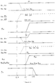
- the internal address bits Ax0 and Axl are low level before the start of the selection operation the potentials at nodes N1, N11, N21 and N31 ar emade high levels by means of respective precharge circuits T1, T11, T21 and T31. Therefore, nodes N2, N12, N22 and N32 are high level and nodes N3, N13, N23, and N33 are low level. Further, since the control signal ⁇ s is high level, the N channel transistors T7, T17, T27 and T37 which constitute the shutdown circuits are in ON state and, thus, nodes N4, N14, N24 and N34 are low level.
- P channel transistor T1, T11, T21 and T31 are turned off when the precharge signal ⁇ p becomes high level.
- the internal address bits Ax0 and Ax1 are made low level to select the word line selection signal ⁇ w1 . Therefore, the N channel transistors T2 and T3 constituting one decode circuit are urned off and thus the node N1 is kept high level. Therefore, the node N2 and the node N3 are kept high level and low level, respectively.
- the nodes N11, N21 and N31 becomes low level.
- the nodes N12, N22 and N32 change their states from high level to low level and the nodes N13, N23 and N33 are changed from low level to high level (see time instant t10 in Fig. 2).
- the word line activating signal ⁇ w becomes as high as or higher than the source voltage (see time instant t11 in Fig. 2)
- potential at the node N2 increases to a level equal to or higher than the source voltage due to the self boot effect of the transistor T5. Therefore, the word line selection signal ⁇ w1 becomes high level equal to or higher than the source voltage, that is, it is activated.
- the transistors T15, T25 and T35 are turned off and, since the nodes N13, N23 and N33 are high level, the transistors T16, T26 and -T36 are turned on, while other word line selection signals are kept low level.
- a word line corresponding thereto is driven and a memory cell (not shown) connected thereto is selected.
- a sense amplifier (not shown)
- large current flows through the ground line and thus the potential thereof is raised temporarily from OV resulting in ground line noise.
- control signal ⁇ s which is an inverted signal of a sense amplifier activating signal becomes low level when the sense amplifier operates (see time instant t12 in Fig. 2) and thus the N channel transistors T7, T17, T27 and T37 constituting the shutdown circuits are turned off. Therefore, all of the decode circuits are disconnected from the ground line. As a result, the nodes N1, N11, N21 and N31 are disconnected from the ground line electrically and thus voltage levels of the word line selection signals ⁇ w1 - ⁇ w4 are not changed.
- the output level of the word line selection signal is not affected by noise generated in the ground line during operation of the memory sense amplifier, since the decode circuits are shutdown with respect to the ground line. Therefore, it is possible to keep the memory cell in a stable selecting condition.
- control signal ⁇ s is obtained by inverting the sense amplifier activating signal.
- any other signal may be used with the same effect provided that its state is changed (from high to low or vice versa) during a time period from the movement at which any of the word line selection signals ⁇ w1 - ⁇ w4 becomes fully high level to a start of operation of the sense amplifier.
- the decode circuit has an NOR circuit construction
- the present invention is not limited thereto.
- the decode circuit may have a NAND circuit construction.
Landscapes
- Engineering & Computer Science (AREA)
- Microelectronics & Electronic Packaging (AREA)
- Dram (AREA)
- Static Random-Access Memory (AREA)
Applications Claiming Priority (2)
| Application Number | Priority Date | Filing Date | Title |
|---|---|---|---|
| JP86248/91 | 1991-03-26 | ||
| JP3086248A JPH04298895A (ja) | 1991-03-26 | 1991-03-26 | 半導体記憶回路 |
Publications (2)
| Publication Number | Publication Date |
|---|---|
| EP0508652A1 true EP0508652A1 (de) | 1992-10-14 |
| EP0508652B1 EP0508652B1 (de) | 1997-07-30 |
Family
ID=13881517
Family Applications (1)
| Application Number | Title | Priority Date | Filing Date |
|---|---|---|---|
| EP92302663A Expired - Lifetime EP0508652B1 (de) | 1991-03-26 | 1992-03-26 | Halbleiterspeicherschaltung |
Country Status (5)
| Country | Link |
|---|---|
| US (1) | US5323357A (de) |
| EP (1) | EP0508652B1 (de) |
| JP (1) | JPH04298895A (de) |
| KR (1) | KR950006300B1 (de) |
| DE (1) | DE69221192T2 (de) |
Cited By (1)
| Publication number | Priority date | Publication date | Assignee | Title |
|---|---|---|---|---|
| US9779679B2 (en) | 2009-07-24 | 2017-10-03 | Semiconductor Energy Laboratory Co., Ltd. | Semiconductor device |
Families Citing this family (7)
| Publication number | Priority date | Publication date | Assignee | Title |
|---|---|---|---|---|
| KR0135231B1 (ko) * | 1994-08-23 | 1998-04-22 | 김주용 | 고속 테스트 기능을 갖는 메모리 소자 |
| US6097218A (en) * | 1996-12-20 | 2000-08-01 | Lsi Logic Corporation | Method and device for isolating noise sensitive circuitry from switching current noise on semiconductor substrate |
| US5764589A (en) * | 1997-03-28 | 1998-06-09 | International Business Machines Corporation | Array row and column decoder apparatus and method |
| US6628552B1 (en) * | 1997-04-11 | 2003-09-30 | Intel Corporation | Self-configuring input buffer on flash memories |
| DE19859516C1 (de) * | 1998-12-22 | 2000-03-02 | Siemens Ag | Integrierte Schaltung mit einem Decoderelement |
| US6240026B1 (en) * | 2000-03-07 | 2001-05-29 | Stmicroelectronics, Inc. | Bit line sense circuit and method for dynamic random access memories |
| US6795367B1 (en) * | 2000-05-16 | 2004-09-21 | Micron Technology, Inc. | Layout technique for address signal lines in decoders including stitched blocks |
Citations (3)
| Publication number | Priority date | Publication date | Assignee | Title |
|---|---|---|---|---|
| US3980899A (en) * | 1974-10-30 | 1976-09-14 | Hitachi, Ltd. | Word line driver circuit in memory circuit |
| EP0017688A1 (de) * | 1979-03-12 | 1980-10-29 | Motorola, Inc. | Monolithische integrierte Schaltung |
| DE3028735C2 (de) * | 1980-07-29 | 1983-06-16 | Siemens AG, 1000 Berlin und 8000 München | Halteschaltung zur definierten Potentialfestlegung von Decodergatterausgängen zur Speicheradressierung |
Family Cites Families (11)
| Publication number | Priority date | Publication date | Assignee | Title |
|---|---|---|---|---|
| US4048629A (en) * | 1975-09-02 | 1977-09-13 | Motorola, Inc. | Low power mos ram address decode circuit |
| JPS6023432B2 (ja) * | 1977-12-09 | 1985-06-07 | 株式会社日立製作所 | Mosメモリ |
| US4259731A (en) * | 1979-11-14 | 1981-03-31 | Motorola, Inc. | Quiet row selection circuitry |
| JPS61144790A (ja) * | 1984-12-18 | 1986-07-02 | Sharp Corp | アドレスデコ−ダ回路 |
| US4620299A (en) * | 1985-03-04 | 1986-10-28 | Motorola, Inc. | Row decoder |
| JPS62231494A (ja) * | 1986-03-31 | 1987-10-12 | Nec Corp | デコ−ダドライバ回路 |
| JPS63228494A (ja) * | 1987-03-18 | 1988-09-22 | Fujitsu Ltd | ダイナミツク型デコ−ダ回路 |
| JPS6452285A (en) * | 1987-08-21 | 1989-02-28 | Mitsubishi Electric Corp | Decoder circuit |
| JP2550684B2 (ja) * | 1988-11-04 | 1996-11-06 | 日本電気株式会社 | 半導体装置 |
| US5245583A (en) * | 1991-04-02 | 1993-09-14 | Vitelic Corporation | Integrated circuit memory with decoded address sustain circuitry for multiplexed address architecture and method |
| US5262687A (en) * | 1992-03-09 | 1993-11-16 | Zilog, Inc. | Decoder circuit with bypass circuitry and reduced input capacitance for greater speed |
-
1991
- 1991-03-26 JP JP3086248A patent/JPH04298895A/ja active Pending
-
1992
- 1992-03-26 US US07/858,191 patent/US5323357A/en not_active Expired - Fee Related
- 1992-03-26 DE DE69221192T patent/DE69221192T2/de not_active Expired - Lifetime
- 1992-03-26 KR KR1019920004926A patent/KR950006300B1/ko not_active Expired - Fee Related
- 1992-03-26 EP EP92302663A patent/EP0508652B1/de not_active Expired - Lifetime
Patent Citations (3)
| Publication number | Priority date | Publication date | Assignee | Title |
|---|---|---|---|---|
| US3980899A (en) * | 1974-10-30 | 1976-09-14 | Hitachi, Ltd. | Word line driver circuit in memory circuit |
| EP0017688A1 (de) * | 1979-03-12 | 1980-10-29 | Motorola, Inc. | Monolithische integrierte Schaltung |
| DE3028735C2 (de) * | 1980-07-29 | 1983-06-16 | Siemens AG, 1000 Berlin und 8000 München | Halteschaltung zur definierten Potentialfestlegung von Decodergatterausgängen zur Speicheradressierung |
Cited By (6)
| Publication number | Priority date | Publication date | Assignee | Title |
|---|---|---|---|---|
| US9779679B2 (en) | 2009-07-24 | 2017-10-03 | Semiconductor Energy Laboratory Co., Ltd. | Semiconductor device |
| US9875713B2 (en) | 2009-07-24 | 2018-01-23 | Semiconductor Energy Laboratory Co., Ltd. | Semiconductor device |
| US10810961B2 (en) | 2009-07-24 | 2020-10-20 | Semiconductor Energy Laboratory Co., Ltd. | Semiconductor device |
| US11373615B2 (en) | 2009-07-24 | 2022-06-28 | Semiconductor Energy Laboratory Co., Ltd. | Semiconductor device |
| US11663989B2 (en) | 2009-07-24 | 2023-05-30 | Semiconductor Energy Laboratory Co., Ltd. | Semiconductor device |
| US12183302B2 (en) | 2009-07-24 | 2024-12-31 | Semiconductor Energy Laboratory Co., Ltd. | Semiconductor device |
Also Published As
| Publication number | Publication date |
|---|---|
| EP0508652B1 (de) | 1997-07-30 |
| US5323357A (en) | 1994-06-21 |
| KR920018754A (ko) | 1992-10-22 |
| JPH04298895A (ja) | 1992-10-22 |
| DE69221192D1 (de) | 1997-09-04 |
| KR950006300B1 (ko) | 1995-06-13 |
| DE69221192T2 (de) | 1997-12-04 |
Similar Documents
| Publication | Publication Date | Title |
|---|---|---|
| US5164621A (en) | Delay device including generator compensating for power supply fluctuations | |
| US5541885A (en) | High speed memory with low standby current | |
| EP0136811A2 (de) | Bitleitungslast und Spalteschaltungen für einen Halbleiterspeicher | |
| KR100312877B1 (ko) | 반도체집적회로장치 | |
| US5574687A (en) | Semiconductor memory | |
| US5537066A (en) | Flip-flop type amplifier circuit | |
| US5699305A (en) | Amplifier and semiconductor memory device having the same | |
| EP0499460B1 (de) | Halbleiterspeicheranordnung | |
| EP0508652B1 (de) | Halbleiterspeicherschaltung | |
| US6292418B1 (en) | Semiconductor memory device | |
| EP0420189B1 (de) | Leseverstärkerschaltung | |
| KR950005171B1 (ko) | 전류 미러 증폭회로 및 그의 구동 방법 | |
| KR0147712B1 (ko) | 에스램의 저전압 동작용 비트 라인 회로 | |
| US5815450A (en) | Semiconductor memory device | |
| US5724299A (en) | Multiport register file memory using small voltage swing for write operation | |
| US5729499A (en) | Sense amplifier and reading circuit with sense amplifier | |
| EP0599275B1 (de) | Integrierte Halbleiterschaltung mit einer Verzögerungsschaltung, die eine zu der Betriebsspannungspannung proportionale Verzögerung aufweist | |
| KR100301602B1 (ko) | 출력파형의링잉을억제하는것이가능한반도체장치 | |
| EP0411818A2 (de) | Stromabfühlverstärker für einen Speicher | |
| IE53368B1 (en) | Mos dynamic memory device | |
| US6046949A (en) | Semiconductor integrated circuit | |
| KR100190366B1 (ko) | 반도체 메모리 장치 및 그 전원인가방법 | |
| JP4322072B2 (ja) | 半導体装置 | |
| JP2912158B2 (ja) | 信号線切替回路 | |
| US6163496A (en) | Semiconductor memory device having a common column decoder shared by plurality of banks |
Legal Events
| Date | Code | Title | Description |
|---|---|---|---|
| PUAI | Public reference made under article 153(3) epc to a published international application that has entered the european phase |
Free format text: ORIGINAL CODE: 0009012 |
|
| 17P | Request for examination filed |
Effective date: 19920421 |
|
| AK | Designated contracting states |
Kind code of ref document: A1 Designated state(s): DE FR GB |
|
| 17Q | First examination report despatched |
Effective date: 19950829 |
|
| GRAG | Despatch of communication of intention to grant |
Free format text: ORIGINAL CODE: EPIDOS AGRA |
|
| GRAH | Despatch of communication of intention to grant a patent |
Free format text: ORIGINAL CODE: EPIDOS IGRA |
|
| GRAH | Despatch of communication of intention to grant a patent |
Free format text: ORIGINAL CODE: EPIDOS IGRA |
|
| GRAA | (expected) grant |
Free format text: ORIGINAL CODE: 0009210 |
|
| AK | Designated contracting states |
Kind code of ref document: B1 Designated state(s): DE FR GB |
|
| REF | Corresponds to: |
Ref document number: 69221192 Country of ref document: DE Date of ref document: 19970904 |
|
| ET | Fr: translation filed | ||
| PLBE | No opposition filed within time limit |
Free format text: ORIGINAL CODE: 0009261 |
|
| STAA | Information on the status of an ep patent application or granted ep patent |
Free format text: STATUS: NO OPPOSITION FILED WITHIN TIME LIMIT |
|
| 26N | No opposition filed | ||
| REG | Reference to a national code |
Ref country code: GB Ref legal event code: IF02 |
|
| REG | Reference to a national code |
Ref country code: GB Ref legal event code: 732E |
|
| REG | Reference to a national code |
Ref country code: FR Ref legal event code: TP |
|
| PGFP | Annual fee paid to national office [announced via postgrant information from national office to epo] |
Ref country code: FR Payment date: 20100324 Year of fee payment: 19 |
|
| PGFP | Annual fee paid to national office [announced via postgrant information from national office to epo] |
Ref country code: GB Payment date: 20100322 Year of fee payment: 19 |
|
| PGFP | Annual fee paid to national office [announced via postgrant information from national office to epo] |
Ref country code: DE Payment date: 20100429 Year of fee payment: 19 |
|
| GBPC | Gb: european patent ceased through non-payment of renewal fee |
Effective date: 20110326 |
|
| REG | Reference to a national code |
Ref country code: FR Ref legal event code: ST Effective date: 20111130 |
|
| PG25 | Lapsed in a contracting state [announced via postgrant information from national office to epo] |
Ref country code: DE Free format text: LAPSE BECAUSE OF NON-PAYMENT OF DUE FEES Effective date: 20111001 Ref country code: FR Free format text: LAPSE BECAUSE OF NON-PAYMENT OF DUE FEES Effective date: 20110331 |
|
| REG | Reference to a national code |
Ref country code: DE Ref legal event code: R119 Ref document number: 69221192 Country of ref document: DE Effective date: 20111001 |
|
| PG25 | Lapsed in a contracting state [announced via postgrant information from national office to epo] |
Ref country code: GB Free format text: LAPSE BECAUSE OF NON-PAYMENT OF DUE FEES Effective date: 20110326 |