EP0508661A1 - Circuit de modulation de fréquence ayant par canal une voie de modulation et une voie de signal separées - Google Patents
Circuit de modulation de fréquence ayant par canal une voie de modulation et une voie de signal separées Download PDFInfo
- Publication number
- EP0508661A1 EP0508661A1 EP92302805A EP92302805A EP0508661A1 EP 0508661 A1 EP0508661 A1 EP 0508661A1 EP 92302805 A EP92302805 A EP 92302805A EP 92302805 A EP92302805 A EP 92302805A EP 0508661 A1 EP0508661 A1 EP 0508661A1
- Authority
- EP
- European Patent Office
- Prior art keywords
- frequency
- signal
- circuit
- channel signal
- channel
- Prior art date
- Legal status (The legal status is an assumption and is not a legal conclusion. Google has not performed a legal analysis and makes no representation as to the accuracy of the status listed.)
- Withdrawn
Links
- 239000013078 crystal Substances 0.000 claims description 5
- 230000004044 response Effects 0.000 description 10
- 238000012937 correction Methods 0.000 description 6
- 238000006243 chemical reaction Methods 0.000 description 5
- 238000010586 diagram Methods 0.000 description 3
- 230000005236 sound signal Effects 0.000 description 3
- 238000000034 method Methods 0.000 description 1
- 238000012986 modification Methods 0.000 description 1
- 230000004048 modification Effects 0.000 description 1
- 210000003813 thumb Anatomy 0.000 description 1
Images

Classifications
-
- H—ELECTRICITY
- H03—ELECTRONIC CIRCUITRY
- H03C—MODULATION
- H03C3/00—Angle modulation
- H03C3/02—Details
- H03C3/09—Modifications of modulator for regulating the mean frequency
- H03C3/0908—Modifications of modulator for regulating the mean frequency using a phase locked loop
- H03C3/095—Modifications of modulator for regulating the mean frequency using a phase locked loop applying frequency modulation to the loop in front of the voltage controlled oscillator
-
- H—ELECTRICITY
- H03—ELECTRONIC CIRCUITRY
- H03C—MODULATION
- H03C3/00—Angle modulation
- H03C3/02—Details
- H03C3/09—Modifications of modulator for regulating the mean frequency
- H03C3/0908—Modifications of modulator for regulating the mean frequency using a phase locked loop
- H03C3/0916—Modifications of modulator for regulating the mean frequency using a phase locked loop with frequency divider or counter in the loop
- H03C3/0925—Modifications of modulator for regulating the mean frequency using a phase locked loop with frequency divider or counter in the loop applying frequency modulation at the divider in the feedback loop
-
- H—ELECTRICITY
- H03—ELECTRONIC CIRCUITRY
- H03C—MODULATION
- H03C3/00—Angle modulation
- H03C3/02—Details
- H03C3/09—Modifications of modulator for regulating the mean frequency
- H03C3/0908—Modifications of modulator for regulating the mean frequency using a phase locked loop
- H03C3/0941—Modifications of modulator for regulating the mean frequency using a phase locked loop applying frequency modulation at more than one point in the loop
-
- H—ELECTRICITY
- H03—ELECTRONIC CIRCUITRY
- H03B—GENERATION OF OSCILLATIONS, DIRECTLY OR BY FREQUENCY-CHANGING, BY CIRCUITS EMPLOYING ACTIVE ELEMENTS WHICH OPERATE IN A NON-SWITCHING MANNER; GENERATION OF NOISE BY SUCH CIRCUITS
- H03B2201/00—Aspects of oscillators relating to varying the frequency of the oscillations
- H03B2201/02—Varying the frequency of the oscillations by electronic means
- H03B2201/0275—Varying the frequency of the oscillations by electronic means the means delivering several selected voltages or currents
- H03B2201/0283—Varying the frequency of the oscillations by electronic means the means delivering several selected voltages or currents the means functioning digitally
-
- H—ELECTRICITY
- H03—ELECTRONIC CIRCUITRY
- H03B—GENERATION OF OSCILLATIONS, DIRECTLY OR BY FREQUENCY-CHANGING, BY CIRCUITS EMPLOYING ACTIVE ELEMENTS WHICH OPERATE IN A NON-SWITCHING MANNER; GENERATION OF NOISE BY SUCH CIRCUITS
- H03B28/00—Generation of oscillations by methods not covered by groups H03B5/00 - H03B27/00, including modification of the waveform to produce sinusoidal oscillations
-
- H—ELECTRICITY
- H03—ELECTRONIC CIRCUITRY
- H03C—MODULATION
- H03C2200/00—Indexing scheme relating to details of modulators or modulation methods covered by H03C
- H03C2200/0004—Circuit elements of modulators
- H03C2200/0029—Memory circuits, e.g. ROMs, RAMs, EPROMs, latches, shift registers
Definitions
- This invention relates to the art of frequency modulation and, more particularly, to a circuit which provides up conversion of a digitally generated frequency modulated signal employing separate modulation and channel signal paths.
- an FM signal generator sometimes referred to as an FM exciter, available as a standby which can be quickly substituted for a signal generator taken out of service and in which the standby signal generator can be quickly tuned to a desired center frequency, such as within the frequency band of from 87.5 MHz to 108 MHz.
- a desired center frequency such as within the frequency band of from 87.5 MHz to 108 MHz.
- the Federal Communications Commission has required that the operation of such FM signal generators be such that the frequency deviation from the center frequency be limited to within ⁇ 0.075 MHz. It is frequently desirable by broadcasters to operate with a frequency deviation approaching as close as possible to the deviation limitation of ⁇ 0.075 MHz in order to achieve maximum "loudness".
- VCO voltage controlled oscillator
- the VCO is set to a desired center frequency within the FM band of 87.5 to 108 MHz.
- the input to the VCO is varied by a modulation signal, such as an audio signal.
- the VCO has a nonlinear frequency deviation response characteristic such that when the signal generator is tuned to a particular center frequency, various signal correction circuits must be adjusted to compensate for the nonlinear frequency deviation response characteristics. This adjustment process is frequently time consuming.
- an FM signal may be generated by digital means such as by a numeric controlled modulated oscillator (NCMO), such as that described in the U.S. Patent to E. W. McCune, 4,746,880.
- NCMO numeric controlled modulated oscillator
- Unlike the VCO, such NCMO devices have linear frequency deviation response characteristics.
- NCMO circuits typically employ digital devices including adders and look-up tables.
- a look-up table may take the form of a programmable read only memory (PROM).
- PROM programmable read only memory
- the operation of such digital devices is limited to clock rates well below the primary radio frequency FM band of 87.5 to 108 MHz.
- such devices typically operate at a lower frequency level, such as on the order of 20 MHz and require an up conversion to a higher frequency if they are to be employed in providing an FM signal in the frequency band of 87.5 to 108 MHz.
- the U.S. Patent to L. J. Avila et al., 4,706,047 discloses a system employing digital means for generating an FM signal at a relatively low frequency together with a phase lock loop (PLL) and which includes a VCO to place the output signal at a higher frequency.
- PLL phase lock loop
- Avila's PLL circuit employs a VCO in the modulation path. Consequently, the VCO employed has a nonlinear frequency deviation response characteristic as discussed hereinabove. This limits the use of such a circuit to an FM signal generator having a fixed center frequency as one cannot quickly retune the signal generator to a different center frequency because time-consuming adjustments are required of correction circuits to correct for the nonlinear frequency deviation response characteristics of the VCO.
- the FM modulator circuit includes a modulation path having a numerically controlled oscillator which receives a modulation signal and provides a frequency modulated intermediate frequency signal which has been frequency modulated in accordance with the modulation signal.
- a channel select number is provided representative of a channel of a desired frequency.
- a channel signal path is provided including local oscillator means for receiving the channel select signal and providing a channel signal of the desired frequency. The modulated intermediate frequency signal is then mixed with the channel signal to provide a frequency up-converted FM output signal.
- Figs. 1 and 2 disclose a prior art FM signal generator and a graphical illustration of control signal amplitude with respect to frequency showing the manner in which the VCO in Fig. 1 operates.
- the prior art FM signal generator 10 in Fig. 1 includes a crystal oscillator 12 which may provide a very accurate reference frequency and which may be on the order of 10 MHz which is then applied to a fixed divider 14 with the output being applied to one input of a phase detector 16.
- This phase detector is part of a phase lock loop (PLL) to be described hereinafter.
- the other input to the phase detector 16 is obtained from a variable divider 18 which divides the output frequency of a voltage controlled oscillator (VCO) 20 by a variable number N.
- VCO voltage controlled oscillator
- the value of N is adjusted by means of a frequency tuner 22.
- the output of the phase detector is then supplied through a low-pass filter 30 and is amplified by an error amplifier 32 which then provides a DC voltage, representative of the required VSO control signal amplitude, to the input of the VCO 20.
- the FM signal obtained from the VCO is fed back to the variable divider in the phase lock loop (PLL) and is also supplied to a power amplifier 34.
- the output frequency of the VCO may be considered frequency F0 and it varies from a center frequency F c in accordance with a modulation signal provided to the VCO by means of a modulation source 36.
- the modulation signal is supplied to a summing point 38 that is actually inside the VCO 20.
- the frequency tuner 22 is operated to adjust the value of N so that the phase lock loop drives the VCO to operate at the desired center frequency F c .
- the VCO exhibits nonlinear frequency deviation response characteristics, as will be noted from reference to Fig. 2.
- curve A represents the frequency control response characteristics of a voltage controlled oscillator, such as VCO 20. It is to be noted that curve A is a nonlinear curve. For example, if an operator is tuning the transmitter to a center frequency F c of a particular frequency value, then this may correspond with an input voltage being supplied to the VCO of a magnitude of V A .
- the FCC has required that broadcasters limit the modulation operation so that the frequency deviation from the center line frequency will not exceed ⁇ 0.075 MHz.
- the lower frequency F L should not deviate from the center frequency F c by more than 0.075 MHz and the upper frequency F U should not exceed the center frequency F c by more than 0.075 MHz.
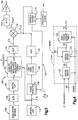
- Fig. 3 illustrates an FM signal generator constructed in accordance with the present invention and in which the center frequency may be easily changed in the field.
- the circuit of Fig. 3 separates the modulation signal path from the channel signal path.
- a modulation path 100 and a channel signal path 102.
- the modulation signal path 100 does not include a VCO, as in the case of the prior art discussed hereinbefore.
- the modulation path 100 includes a numeric controlled modulated oscillator (NCMO) 104 which includes digital means for generating a frequency modulated signal.
- NCMO numeric controlled modulated oscillator
- NCMO 104 may be obtained from Digital RF Solutions Corporation of Santa Clara, California, and which device is described in the U.S. Patent to E. W. McCune, Jr., 4,746,880.
- the modulation input to the NCMO 104 is usually digitized from an analog modulation source 106, which may include an audio signal.
- the audio signal from the modulation source 106 is converted by an analog-to-digital converter 108 into a multi-bit digital word, such as 24 bits, which is then passed through a digital correction filter 110 to remove non-ideal characteristics from the digitized signal, supplying a digitized 24 bit modulation signal to the input of the NCMO 104.
- a crystal oscillator 112 provides a clock signal and which may have a frequency on the order of 10 MHz and this is supplied to the clock input of the NCMO which then digitally generates a multi-bit (12 bit) frequency modulated signal and which is then converted to an analog signal by a digital-to-analog converter 114 and supplied to one input of a mixer 116.
- the NCMO 104 has an input for receiving a control number representing the desired IF frequency.
- the numeric controlled oscillator NCMO 104 preferably takes the form as described in the McCune patent discussed hereinabove.
- a simplified showing of such an NCMO 104 is illustrated in Fig. 4, from which it is seen that the multi-bit digitized modulation signal is supplied to a digital adder 120, the output of which is supplied to a second digital adder operating as a phase accumulator and which provides a 24 bit address to a look-up table 124 and which may take the form of a programmable read only memory (PROM).
- PROM programmable read only memory
- the operation of the NCMO is limited in its frequency to the maximum clock rate at which the digital components may operate including the time required to read values from the look-up table 124 to provide a 12 bit digital output.
- This is considerably below the radio frequency modulation band of 87.5 MHz to 108 MHz.
- the NCMO may operate at a relatively low center frequency F c such as on the order of 3 MHz. Since the frequency deviation response characteristics are linear, the modulation may be set for the maximum allowed level, which for the United States is ⁇ 0.075 MHz relative to the center frequency F c .
- the output frequency of the digital-to-analog converter 114 may be considered as an intermediate frequency F IF . This needs to be raised to a higher frequency in the radio frequency band of 87.5 MHz to 108 MHz. This is achieved with the circuitry to be described below.
- the up-conversion circuitry of Fig. 3 includes a separate channel signal path 102 and which includes a local oscillator which produces a channel frequency signal F LO which, when combined with the output frequency signal F IF , provides a center frequency of the desired operating frequency for the broadcast station. For example, if it is intended that the broadcast station have a center frequency of 102 MHz and if the center frequency of the intermediate frequency signal F IF is on the order of 3 MHz, then it is clear that the channel frequency signal F LO must be adjusted to exactly 99.0 MHz, or its equivalent using multiple conversions according to general and common practice. This is achieved with the described signal conversion circuitry discussed below.
- the channel select path includes a VCO 130 located in the phase lock loop (PLL) and which includes a variable divider 132, a phase detector 134 and a low-pass filter 136 all connected as illustrated in Fig. 3.
- the operator will adjust a frequency tuner 140, such as a conventional thumb wheel switch, to vary the value of N so as to divide the output frequency F LO obtained from the voltage controlled oscillator by the number N.
- the phase detector compares the output signal F IN of the crystal oscillator with the output of the variable divider, which is F LO divided by N, and adjusts the operation of the VCO until the two signals match.
- the local oscillator signal F LO is then supplied to the mixer 116 where it is mixed with the intermediate frequency signal F IF to obtain an output frequency signal F OUT which is then passed through a bandpass filter 144 which passes the frequencies in a select band within the FM bandwidth of 87.5 MHz to 108 MHz with the output signal then being supplied to a suitable power amplifier 146.
- both the modulation path 100 and the channel signal path 102 may be individually and independently optimized. This permits direct application of numeric modulation to achieve the full signal modulation specification.
- the modulation path is optimized for linearity and allows for use of an accurate numeric controlled oscillator which has a linear frequency deviation response characteristic.
- the VCO is set to operate at only one specific frequency, as no frequency deviations or modulations are involved in the operation of the VCO.
- the bandwidth of the phase lock loop may be set to optimize for output noise. Also, by providing the separate channel signal path, fast lock up times may be achieved with significantly reduced microphonics.
Landscapes
- Stabilization Of Oscillater, Synchronisation, Frequency Synthesizers (AREA)
- Transmitters (AREA)
Applications Claiming Priority (2)
| Application Number | Priority Date | Filing Date | Title |
|---|---|---|---|
| US68398291A | 1991-04-11 | 1991-04-11 | |
| US683982 | 1991-04-11 |
Publications (1)
| Publication Number | Publication Date |
|---|---|
| EP0508661A1 true EP0508661A1 (fr) | 1992-10-14 |
Family
ID=24746238
Family Applications (1)
| Application Number | Title | Priority Date | Filing Date |
|---|---|---|---|
| EP92302805A Withdrawn EP0508661A1 (fr) | 1991-04-11 | 1992-03-30 | Circuit de modulation de fréquence ayant par canal une voie de modulation et une voie de signal separées |
Country Status (3)
| Country | Link |
|---|---|
| EP (1) | EP0508661A1 (fr) |
| JP (1) | JPH05211449A (fr) |
| CA (1) | CA2065816A1 (fr) |
Cited By (5)
| Publication number | Priority date | Publication date | Assignee | Title |
|---|---|---|---|---|
| EP0631378A1 (fr) * | 1993-06-24 | 1994-12-28 | Robert Bosch Gmbh | Procédé de modulation de fréquence |
| EP0632576A1 (fr) * | 1993-06-24 | 1995-01-04 | Robert Bosch Gmbh | Procédé de modulation de fréquence |
| DE4320996A1 (de) * | 1993-06-24 | 1995-01-05 | Ant Nachrichtentech | Verfahren zur Frequenzmodulation |
| EP0631377A3 (fr) * | 1993-06-24 | 1995-11-08 | Ant Nachrichtentech | Procédé de modulation de fréquence. |
| EP0631376A3 (fr) * | 1993-06-24 | 1995-11-08 | Ant Nachrichtentech | Procédé de modulation de fréquence. |
Citations (4)
| Publication number | Priority date | Publication date | Assignee | Title |
|---|---|---|---|---|
| EP0036431A1 (fr) * | 1979-09-27 | 1981-09-30 | Toyo Communication Equipment Co.,Ltd. | Emetteur ayant une boucle a phase verrouillee |
| US4706047A (en) * | 1986-12-01 | 1987-11-10 | Ford Aerospace & Communications Corporation | Frequency extended digitally generated FM |
| US4746880A (en) * | 1987-02-06 | 1988-05-24 | Digital Rf Solutions Corporation | Number controlled modulated oscillator |
| US5010585A (en) * | 1990-06-01 | 1991-04-23 | Garcia Rafael A | Digital data and analog radio frequency transmitter |
-
1992
- 1992-03-30 EP EP92302805A patent/EP0508661A1/fr not_active Withdrawn
- 1992-04-10 CA CA002065816A patent/CA2065816A1/fr not_active Abandoned
- 1992-04-13 JP JP4093061A patent/JPH05211449A/ja active Pending
Patent Citations (4)
| Publication number | Priority date | Publication date | Assignee | Title |
|---|---|---|---|---|
| EP0036431A1 (fr) * | 1979-09-27 | 1981-09-30 | Toyo Communication Equipment Co.,Ltd. | Emetteur ayant une boucle a phase verrouillee |
| US4706047A (en) * | 1986-12-01 | 1987-11-10 | Ford Aerospace & Communications Corporation | Frequency extended digitally generated FM |
| US4746880A (en) * | 1987-02-06 | 1988-05-24 | Digital Rf Solutions Corporation | Number controlled modulated oscillator |
| US5010585A (en) * | 1990-06-01 | 1991-04-23 | Garcia Rafael A | Digital data and analog radio frequency transmitter |
Cited By (5)
| Publication number | Priority date | Publication date | Assignee | Title |
|---|---|---|---|---|
| EP0631378A1 (fr) * | 1993-06-24 | 1994-12-28 | Robert Bosch Gmbh | Procédé de modulation de fréquence |
| EP0632576A1 (fr) * | 1993-06-24 | 1995-01-04 | Robert Bosch Gmbh | Procédé de modulation de fréquence |
| DE4320996A1 (de) * | 1993-06-24 | 1995-01-05 | Ant Nachrichtentech | Verfahren zur Frequenzmodulation |
| EP0631377A3 (fr) * | 1993-06-24 | 1995-11-08 | Ant Nachrichtentech | Procédé de modulation de fréquence. |
| EP0631376A3 (fr) * | 1993-06-24 | 1995-11-08 | Ant Nachrichtentech | Procédé de modulation de fréquence. |
Also Published As
| Publication number | Publication date |
|---|---|
| JPH05211449A (ja) | 1993-08-20 |
| CA2065816A1 (fr) | 1992-10-12 |
Similar Documents
| Publication | Publication Date | Title |
|---|---|---|
| US5313173A (en) | Quadrature modulated phase-locked loop | |
| US4451930A (en) | Phase-locked receiver with derived reference frequency | |
| US8655296B2 (en) | Frequency synthesizer and related method for generating wideband signals | |
| US6298093B1 (en) | Apparatus and method for phase and frequency digital modulation | |
| US4211975A (en) | Local signal generation arrangement | |
| US20040196924A1 (en) | Radio transmitter architecture comprising a PLL and a delta-sigma modulator | |
| US7391839B2 (en) | Accumulator based phase locked loop | |
| US4737968A (en) | QPSK transmission system having phaselocked tracking filter for spectrum shaping | |
| WO1992020144A1 (fr) | Synthetiseur de frequence numerique possedant un systeme de commande automatique de frequence (caf) et un systeme de modulation appliquee a un diviseur de frequence | |
| US6345173B1 (en) | Frequency modulator | |
| US4117422A (en) | Circuit for compensating vco nonlinearities in frequency modulated phase-locked loops and method thereof | |
| US5424688A (en) | Frequency synthesizer apparatus incorporating phase modulation tracking means | |
| US5706310A (en) | Wide bandwidth loop in a frequency shift keying (FSK) system | |
| EP0082473A2 (fr) | Emetteur à modulation de fréquence | |
| US7167528B2 (en) | Modulation system for modulating data onto a carrier signal with offsets to compensate for doppler effect and allow a frequency synthesizing system to make steps equal to channel bandwidth | |
| EP0508661A1 (fr) | Circuit de modulation de fréquence ayant par canal une voie de modulation et une voie de signal separées | |
| JP2006505196A (ja) | 信号の周波数を変換するためのシステムおよび方法 | |
| JP2004032688A (ja) | チューナー | |
| US6091943A (en) | Combining oscillator with a phase-indexed control circuit for a radio receiver | |
| CA2118810C (fr) | Appareil radio a boucles d'asservissement de phase et de commande automatique de frequence combinees et methode d'utilisation de cet appareil | |
| US20050058219A1 (en) | Apparatus, methods and articles of manufacture for pre-emphasis filtering of a modulated signal | |
| US4739288A (en) | Combined phase and frequency modulator for modulating an information signal | |
| US7158603B2 (en) | Method and apparatus for compensating deviation variances in a 2-level FSK FM transmitter | |
| CN112968857A (zh) | 一种海事中频发射机射频激励器 | |
| US6433830B1 (en) | Off-air phase lock technique |
Legal Events
| Date | Code | Title | Description |
|---|---|---|---|
| PUAI | Public reference made under article 153(3) epc to a published international application that has entered the european phase |
Free format text: ORIGINAL CODE: 0009012 |
|
| AK | Designated contracting states |
Kind code of ref document: A1 Designated state(s): DE FR IT |
|
| 17P | Request for examination filed |
Effective date: 19930330 |
|
| STAA | Information on the status of an ep patent application or granted ep patent |
Free format text: STATUS: THE APPLICATION IS DEEMED TO BE WITHDRAWN |
|
| 18D | Application deemed to be withdrawn |
Effective date: 19941004 |