EP0508759A2 - Procédé de formation de contacts submicroscopiques, à côtés inclinés de perte donnée réalisés par décapage - Google Patents
Procédé de formation de contacts submicroscopiques, à côtés inclinés de perte donnée réalisés par décapage Download PDFInfo
- Publication number
- EP0508759A2 EP0508759A2 EP92303133A EP92303133A EP0508759A2 EP 0508759 A2 EP0508759 A2 EP 0508759A2 EP 92303133 A EP92303133 A EP 92303133A EP 92303133 A EP92303133 A EP 92303133A EP 0508759 A2 EP0508759 A2 EP 0508759A2
- Authority
- EP
- European Patent Office
- Prior art keywords
- opening
- layer
- photoresist layer
- photoresist
- forming
- Prior art date
- Legal status (The legal status is an assumption and is not a legal conclusion. Google has not performed a legal analysis and makes no representation as to the accuracy of the status listed.)
- Withdrawn
Links
Images

Classifications
-
- H—ELECTRICITY
- H10—SEMICONDUCTOR DEVICES; ELECTRIC SOLID-STATE DEVICES NOT OTHERWISE PROVIDED FOR
- H10W—GENERIC PACKAGES, INTERCONNECTIONS, CONNECTORS OR OTHER CONSTRUCTIONAL DETAILS OF DEVICES COVERED BY CLASS H10
- H10W20/00—Interconnections in chips, wafers or substrates
- H10W20/01—Manufacture or treatment
- H10W20/071—Manufacture or treatment of dielectric parts thereof
- H10W20/081—Manufacture or treatment of dielectric parts thereof by forming openings in the dielectric parts
- H10W20/082—Manufacture or treatment of dielectric parts thereof by forming openings in the dielectric parts the openings being tapered via holes
-
- H—ELECTRICITY
- H10—SEMICONDUCTOR DEVICES; ELECTRIC SOLID-STATE DEVICES NOT OTHERWISE PROVIDED FOR
- H10P—GENERIC PROCESSES OR APPARATUS FOR THE MANUFACTURE OR TREATMENT OF DEVICES COVERED BY CLASS H10
- H10P50/00—Etching of wafers, substrates or parts of devices
- H10P50/73—Etching of wafers, substrates or parts of devices using masks for insulating materials
-
- H—ELECTRICITY
- H10—SEMICONDUCTOR DEVICES; ELECTRIC SOLID-STATE DEVICES NOT OTHERWISE PROVIDED FOR
- H10W—GENERIC PACKAGES, INTERCONNECTIONS, CONNECTORS OR OTHER CONSTRUCTIONAL DETAILS OF DEVICES COVERED BY CLASS H10
- H10W20/00—Interconnections in chips, wafers or substrates
- H10W20/01—Manufacture or treatment
- H10W20/071—Manufacture or treatment of dielectric parts thereof
- H10W20/081—Manufacture or treatment of dielectric parts thereof by forming openings in the dielectric parts
- H10W20/084—Manufacture or treatment of dielectric parts thereof by forming openings in the dielectric parts for dual-damascene structures
Definitions
- the present invention relates generally to semiconductor integrated circuit processing, and more specifically to producing submicron contacts with unique etched slopes.
- photolithography has become one of the most critical steps in semiconductor manufacturing.
- the goal of photolithography in establishing the horizontal dimensions of the various devices and circuits is to create a pattern which meets design requirements as well as to correctly align the circuit pattern on the surface of the wafer.
- Exposure light sources are chosen in photolithography based upon the characteristics of the photoresist.
- Standard production exposure tools used to print contact holes may limit how small the holes can be made.
- One problem with standard exposure tools is in the auto focus mechanism used to pattern a wafer.
- the exposure tools, when used in conjunction with thick photoresists have a small depth of focus so that light focused on the top of the photoresist will be out of focus near the bottom of the photoresist.
- Diffraction reduces the resolution of an image in the photoresist causing poor image definition.
- Image resolution known as latent image decay, may also be reduced through the addition of chemicals to the photoresist.
- the focus problem of standard production exposure tools causes poor control of the pattern imaged into the photoresist and the light needed to expose the photoresist at the bottom of the contact hole nearest the wafer.
- An increase in the exposure light dose to overcome this focus problem allows incident light to expose areas of the photoresist that are not targeted for exposure. Any increase in exposure time to compensate for the focus problem cannot control the incident light, resulting in poor photoresist sidewall profiles. These profiles generally result in an opening too large at the top of the photoresist causing poor circuit overlay to the underlying wafer.
- submicron contact openings are made by forming an insulating layer over a substrate and a photoresist layer over the insulating layer.
- the thick photoresist layer is patterned and etched to form a first opening in the photoresist.
- a thin photoresist layer is then formed over the integrated circuit which is then patterned and etched to form a second opening inside the first opening.
- a contact opening is then etched through the insulating layer through the second opening in the thin photoresist.
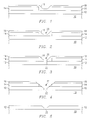
- an integrated circuit is to be formed in a silicon substrate 10 .
- Selected regions of the substrate 10 are oxidized to form an insulating layer of oxide 12 .
- a first layer of photoresist 14 is formed on the integrated circuit by known methods.
- Photoresist layer 14 will have a thickness of approximately 1.2 microns.
- Photoresist layer 14 is then patterned and etched by methods known in the art to form a first opening 16.
- a second photoresist layer 18 is then spun onto the wafer again by known methods covering the first photoresist layer 14 and opening 16 .
- Photoresist layer 18 has a smaller thickness of between approximately 0.1 to 0.5 microns.
- photoresist layer 18 is patterned and etched by methods known in the art to form a second opening 20 .
- Opening 20 has a smaller opening than 16 and is inside opening 16 .
- Photoresist coating chemicals used for standard processing may be used for photoresist layers 14 and 18 .
- the chemical composition of photoresist layer 14 may be the same or different than the chemical composition of photoresist layer 18 .
- contact opening 22 is etched using a standard dry etch process known in the art.
- the selectivity of the etchant used will determine the preservation of the substrate surface 10 underlying the oxide layer 12 and the profile of the vertical sides of the contact opening 22 and the remaining photoresist layers 14 and 18 .
- a highly selective etchant will not substantially change the profile or shape of the vertical sides of the contact opening 22 as shown in Figure 3 .
- the etch rate for the contact opening 22 will be greater than the etch rate of photoresist layer 18 so that the contact opening is etched before the photoresist layer is etched.
- a poorly selective etchant or a non-selective etchant will attack the resist and change the shape or profile of the vertical sides of the contact opening as shown in Figure 4 .
- the etch rate of the oxide layer 12 will be similar to the etch rate for photoresist layer 18 . This anisotropic dry etch will result in an oxide profile similar to the photoresist layer profile.
- the remaining photoresist layers 14 and 18 are stripped away using a process known in the art leaving the contact opening 22 through the oxide layer 12 as shown in Figure 5 .
- the steps described above eliminate the need for wet etching using only a dry etching process while maintaining a desired sloped contact.
- an alternative method for producing submicron contacts with unique etched slopes uses an insulating layer as a mask.
- An integrated circuit is to be formed in a silicon substrate 24 .
- An insulating layer of oxide 26 is formed on the substrate 24 .
- a layer of photoresist 28 is spun onto the integrated circuit by known methods.
- Photoresist layer 28 will typically have a thickness of approximately 1.2 microns.
- After photoresist layer 28 is patterned to define a contact opening 32 the portions of the oxide layer 26 exposed through opening 32 is etched. The etch process stops when the oxide layer 26 is partially etched. This etching process will further etch partway through the oxide layer 26 .
- Photoresist layer 28 is then removed by known methods.
- a second photoresist layer 30 is then spun onto the wafer by methods known in the art.
- Photoresist layer 30 is patterned and etched to form a small opening 34 within the larger opening 32 . This etching process will etch the remaining way through the oxide layer 26 to form a contact opening 36 .
- the selectivity of the etchant used will determine the preservation of the substrate surface 24 underlying the oxide layer 26 and the profile of the vertical sides of the contact opening 36 and the photoresist layer 30 .
- a highly selective etchant will not substantially change the profile of the vertical sides of the contact opening 34 as shown in Figure 7 .
- the etch rate for the contact opening 34 will be greater than the etch rate of photoresist layer 30 so that the contact opening is etched before the photoresist layer is etched.
- a poorly selective etchant or a non-selective etchant will attack the resist and change the shape or profile of the vertical sides of the contact opening as shown in Figure 8 .
- the etch rate of the oxide layer 26 will be similar to the etch rate for photoresist layer 30 .
- This anisotropic dry etch will result in an oxide profile similar to the photoresist layer profile.
- Photoresist layer 30 is then stripped away using a process known in the art leaving the contact opening 36 through the oxide layer 26 as shown in Figure 9 .
- the anisotropic dry etch process will provide for sloped sidewalls and insure adequate step coverage.
- the method described above does not require the use of special photoresist chemicals.
- the chemical composition of the two layers of photoresist may be the same or may have different compositions.
- Standard development, etch and exposure tools and techniques may also be used for this process. There is no need for plasma development, X-ray exposures or other special processing. While current process techniques use a combination wet and dry etch to form slopes on contact holes, this process eliminates the wet etch step. Only dry etches are used while maintaining a desired sloped contact.
- This process can alternatively use the existing device oxide film as a masking barrier instead of a two- tiered photoresist layer. The oxide is patterned and etched and then repatterned and re-etched to form the submicron contacts.
Landscapes
- Drying Of Semiconductors (AREA)
- Internal Circuitry In Semiconductor Integrated Circuit Devices (AREA)
- Electrodes Of Semiconductors (AREA)
Applications Claiming Priority (2)
| Application Number | Priority Date | Filing Date | Title |
|---|---|---|---|
| US68256891A | 1991-04-09 | 1991-04-09 | |
| US682568 | 1991-04-09 |
Publications (2)
| Publication Number | Publication Date |
|---|---|
| EP0508759A2 true EP0508759A2 (fr) | 1992-10-14 |
| EP0508759A3 EP0508759A3 (en) | 1992-12-16 |
Family
ID=24740252
Family Applications (1)
| Application Number | Title | Priority Date | Filing Date |
|---|---|---|---|
| EP19920303133 Withdrawn EP0508759A3 (en) | 1991-04-09 | 1992-04-08 | Method of producing submicron contacts with unique etched slopes |
Country Status (3)
| Country | Link |
|---|---|
| US (1) | US5366848A (fr) |
| EP (1) | EP0508759A3 (fr) |
| JP (1) | JPH05114577A (fr) |
Families Citing this family (5)
| Publication number | Priority date | Publication date | Assignee | Title |
|---|---|---|---|---|
| KR100223325B1 (ko) * | 1995-12-15 | 1999-10-15 | 김영환 | 반도체 장치의 미세패턴 제조방법 |
| KR100414949B1 (ko) * | 1996-12-28 | 2004-03-31 | 주식회사 하이닉스반도체 | 반도체소자의콘택홀형성방법 |
| JP3818188B2 (ja) * | 2002-03-22 | 2006-09-06 | Tdk株式会社 | マスクパターンの形成方法、該マスクパターンを用いたパターニング方法及び薄膜磁気ヘッドの製造方法 |
| US7316971B2 (en) * | 2004-09-14 | 2008-01-08 | International Business Machines Corporation | Wire bond pads |
| DE102009032854B4 (de) * | 2009-07-13 | 2015-07-23 | Texas Instruments Deutschland Gmbh | Verfahren zur Herstellung von Bipolartransistorstrukturen in einem Halbleiterprozess |
Family Cites Families (5)
| Publication number | Priority date | Publication date | Assignee | Title |
|---|---|---|---|---|
| US3518084A (en) * | 1967-01-09 | 1970-06-30 | Ibm | Method for etching an opening in an insulating layer without forming pinholes therein |
| US3873361A (en) * | 1973-11-29 | 1975-03-25 | Ibm | Method of depositing thin film utilizing a lift-off mask |
| JPS58179526A (ja) * | 1982-04-13 | 1983-10-20 | Yoshida Kogyo Kk <Ykk> | コイル状フアスナ−エレメント成形装置 |
| US4789760A (en) * | 1985-04-30 | 1988-12-06 | Advanced Micro Devices, Inc. | Via in a planarized dielectric and process for producing same |
| US4694565A (en) * | 1986-04-28 | 1987-09-22 | Rockwell International Corporation | Method of making hardened CMOS sub-micron field effect transistors |
-
1992
- 1992-04-08 EP EP19920303133 patent/EP0508759A3/en not_active Withdrawn
- 1992-04-08 JP JP4086872A patent/JPH05114577A/ja active Pending
-
1993
- 1993-04-01 US US08/041,524 patent/US5366848A/en not_active Expired - Lifetime
Also Published As
| Publication number | Publication date |
|---|---|
| JPH05114577A (ja) | 1993-05-07 |
| EP0508759A3 (en) | 1992-12-16 |
| US5366848A (en) | 1994-11-22 |
Similar Documents
| Publication | Publication Date | Title |
|---|---|---|
| US6093508A (en) | Dual damascene structure formed in a single photoresist film | |
| US4707218A (en) | Lithographic image size reduction | |
| US5902704A (en) | Process for forming photoresist mask over integrated circuit structures with critical dimension control | |
| KR100420910B1 (ko) | 중간층리소그래피 | |
| KR100323161B1 (ko) | 기판상의 특징부 형성 방법, 트렌치 및 비아 제조 방법, 자기 정렬된 도선 및 상호 접속체 제조 방법 | |
| US20010038972A1 (en) | Ultra-thin resist shallow trench process using metal hard mask | |
| EP0780894A2 (fr) | Procédé de fabrication de trous et de contacts submicroniques dans un circuit intégré | |
| US20010014512A1 (en) | Ultra-thin resist shallow trench process using high selectivity nitride etch | |
| US4758305A (en) | Contact etch method | |
| KR100434133B1 (ko) | 중간층리쏘그래피 | |
| JPH09205145A (ja) | 集積回路及びその製造方法 | |
| KR100443064B1 (ko) | 집적 회로내의 소규모 구조 형성을 위한 이미지 리버설 방법 | |
| EP1181714A1 (fr) | Procede de production de petits espaces et de cellules de memoire a haute densite a l'aide d'une separation nitruree | |
| US5366848A (en) | Method of producing submicron contacts with unique etched slopes | |
| KR20010017560A (ko) | 이중 다마신 구조 형성 방법 | |
| US20080020327A1 (en) | Method of formation of a damascene structure | |
| US6214737B1 (en) | Simplified sidewall formation for sidewall patterning of sub 100 nm structures | |
| JP2778996B2 (ja) | 半導体装置の製造方法 | |
| EP0525942A2 (fr) | Procédé de fabrication d'un circuit intégré utilisant deux couches de matériau de réserve | |
| JP3585039B2 (ja) | ホール形成方法 | |
| WO2002043140A2 (fr) | Couche d'imagerie utile en tant que masque dur destine a des materiaux organiques a faible constante dielectrique | |
| KR940002297B1 (ko) | 다층레지스트를 이용한 패턴형성방법 | |
| EP0554123A1 (fr) | Procédé de fabrication d'un contact | |
| KR100598308B1 (ko) | 반도체 소자의 다마신 패턴 형성방법 | |
| KR0144229B1 (ko) | 반도체 소자의 미세 콘택 형성 방법 |
Legal Events
| Date | Code | Title | Description |
|---|---|---|---|
| PUAI | Public reference made under article 153(3) epc to a published international application that has entered the european phase |
Free format text: ORIGINAL CODE: 0009012 |
|
| AK | Designated contracting states |
Kind code of ref document: A2 Designated state(s): DE FR GB IT |
|
| PUAL | Search report despatched |
Free format text: ORIGINAL CODE: 0009013 |
|
| AK | Designated contracting states |
Kind code of ref document: A3 Designated state(s): DE FR GB IT |
|
| 17P | Request for examination filed |
Effective date: 19930610 |
|
| 17Q | First examination report despatched |
Effective date: 19950223 |
|
| STAA | Information on the status of an ep patent application or granted ep patent |
Free format text: STATUS: THE APPLICATION IS DEEMED TO BE WITHDRAWN |
|
| 18D | Application deemed to be withdrawn |
Effective date: 19950706 |