EP0509246B1 - Rundsteuerempfänger - Google Patents
Rundsteuerempfänger Download PDFInfo
- Publication number
- EP0509246B1 EP0509246B1 EP92104394A EP92104394A EP0509246B1 EP 0509246 B1 EP0509246 B1 EP 0509246B1 EP 92104394 A EP92104394 A EP 92104394A EP 92104394 A EP92104394 A EP 92104394A EP 0509246 B1 EP0509246 B1 EP 0509246B1
- Authority
- EP
- European Patent Office
- Prior art keywords
- frequency
- filter
- ripple
- control receiver
- digital
- Prior art date
- Legal status (The legal status is an assumption and is not a legal conclusion. Google has not performed a legal analysis and makes no representation as to the accuracy of the status listed.)
- Expired - Lifetime
Links
Images
Classifications
-
- H—ELECTRICITY
- H02—GENERATION; CONVERSION OR DISTRIBUTION OF ELECTRIC POWER
- H02J—ELECTRIC POWER NETWORKS; CIRCUIT ARRANGEMENTS OR SYSTEMS FOR SUPPLYING OR DISTRIBUTING ELECTRIC POWER; SYSTEMS FOR STORING ELECTRIC ENERGY
- H02J13/00—Circuit arrangements for providing remote monitoring or remote control of equipment in a power distribution network
- H02J13/13—Circuit arrangements for providing remote monitoring or remote control of equipment in a power distribution network characterised by the transmission of data to equipment in the power network
- H02J13/1311—Circuit arrangements for providing remote monitoring or remote control of equipment in a power distribution network characterised by the transmission of data to equipment in the power network using the power network as support for the transmission
- H02J13/1313—Circuit arrangements for providing remote monitoring or remote control of equipment in a power distribution network characterised by the transmission of data to equipment in the power network using the power network as support for the transmission using pulsed signals
-
- Y—GENERAL TAGGING OF NEW TECHNOLOGICAL DEVELOPMENTS; GENERAL TAGGING OF CROSS-SECTIONAL TECHNOLOGIES SPANNING OVER SEVERAL SECTIONS OF THE IPC; TECHNICAL SUBJECTS COVERED BY FORMER USPC CROSS-REFERENCE ART COLLECTIONS [XRACs] AND DIGESTS
- Y02—TECHNOLOGIES OR APPLICATIONS FOR MITIGATION OR ADAPTATION AGAINST CLIMATE CHANGE
- Y02E—REDUCTION OF GREENHOUSE GAS [GHG] EMISSIONS, RELATED TO ENERGY GENERATION, TRANSMISSION OR DISTRIBUTION
- Y02E60/00—Enabling technologies; Technologies with a potential or indirect contribution to GHG emissions mitigation
-
- Y—GENERAL TAGGING OF NEW TECHNOLOGICAL DEVELOPMENTS; GENERAL TAGGING OF CROSS-SECTIONAL TECHNOLOGIES SPANNING OVER SEVERAL SECTIONS OF THE IPC; TECHNICAL SUBJECTS COVERED BY FORMER USPC CROSS-REFERENCE ART COLLECTIONS [XRACs] AND DIGESTS
- Y04—INFORMATION OR COMMUNICATION TECHNOLOGIES HAVING AN IMPACT ON OTHER TECHNOLOGY AREAS
- Y04S—SYSTEMS INTEGRATING TECHNOLOGIES RELATED TO POWER NETWORK OPERATION, COMMUNICATION OR INFORMATION TECHNOLOGIES FOR IMPROVING THE ELECTRICAL POWER GENERATION, TRANSMISSION, DISTRIBUTION, MANAGEMENT OR USAGE, i.e. SMART GRIDS
- Y04S40/00—Systems for electrical power generation, transmission, distribution or end-user application management characterised by the use of communication or information technologies, or communication or information technology specific aspects supporting them
- Y04S40/12—Systems for electrical power generation, transmission, distribution or end-user application management characterised by the use of communication or information technologies, or communication or information technology specific aspects supporting them characterised by data transport means between the monitoring, controlling or managing units and monitored, controlled or operated electrical equipment
- Y04S40/121—Systems for electrical power generation, transmission, distribution or end-user application management characterised by the use of communication or information technologies, or communication or information technology specific aspects supporting them characterised by data transport means between the monitoring, controlling or managing units and monitored, controlled or operated electrical equipment using the power network as support for the transmission
Definitions
- the invention relates to a ripple control receiver with a prefilter and a digital bandpass filter with an upstream analog / digital converter.
- the invention has set itself the task of avoiding these disadvantages of the known ripple control receivers and achieves this in that the tuned to the ripple control frequency
- the center frequency of one of the higher-frequency passbands of the digital bandpass filter is equal to both a higher image frequency of the sampling frequency of the analog / digital converter and the center frequency of the pre-filter which suppresses the mains frequency and is designed as a bandpass filter.
- the invention takes advantage of the fact that digital bandpass filters have, in addition to the pass band which is tuned to the fundamental frequency and arranged symmetrically to this fundamental frequency, further pass bands which have the odd multiple frequencies of the fundamental frequency as center frequencies.
- the selection of a correspondingly higher ripple control frequency can also be achieved at a low sampling frequency by means of a higher-frequency pass band of the digital bandpass filter.
- the pre-filter is designed as a discrete-time filter, the clock frequency of which is controlled by the evaluating microcomputer and can thus be adapted to the ripple control frequency, analog low-pass filters being provided for band limitation of the discrete-time filter output signals.
- the digital band filter in the evaluating microcomputer of the ripple control receiver, the microcomputer being an 8-bit computer. It is also appropriate to use an 8-bit converter as an analog / digital converter, which is integrated in the microcomputer.
- the pre-filter can also be designed as a computing filter or as a switch-capacitor filter.
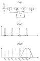
- 1 shows the basic structure of the filter of a ripple control receiver as an exemplary embodiment of the invention.
- 2 and 3 show the filter curves required for the explanation of the invention.
- the mains voltage is at input E of the filter circuit shown in FIG. 1.
- a voltage level suitable for processing in the filter circuit is obtained by means of a voltage divider SP.
- the 50 Hz mains frequency is filtered out by means of a connected prefilter VF, and the frequency mixture freed from the mains frequency is fed to an analog / digital converter ADW.
- a downstream bandpass filter BF is tuned with its center frequency to the ripple control frequency Rf and delivers a signal to a connected decoder DEC, from which the decoder DEC recognizes whether the ripple control signal is present or not. Accordingly, the decoder DEC delivers at its output A a binary signal which in its entirety represents the ripple control signal which is further processed by a connected pulse evaluation circuit, which is not shown.
- TG is a clock generator that supplies the sampling clock pulses for all connected devices.
- the mode of operation of the filter arrangement according to the invention is based on the fact that the bandpass filter BF which selects the ripple control frequency Rf has a plurality of passbands which are entered in the diagram of FIG. 2 over the frequency f. With f A the sampling frequency of the analog / digital converter ADW is designated. The fundamental frequency and at the same time the center frequency of the first pass band of the bandpass filter BF is equal to the frequency f A / 4. The further passbands of the bandpass filter BF have the odd multiples of the fundamental frequency f A / 4 as center frequencies, that is 3f A / 4, 5f A / 4 and 7f A / 4.
- the higher-frequency passband of the bandpass filter BF is therefore substantially higher than the sampling frequency f A of the analog / digital converter ADW, ie vice versa, that the sampling frequency f A can be chosen so low that the advantages mentioned for the computing speed result. which in turn enable the use of cheap microprocessors.
Landscapes
- Engineering & Computer Science (AREA)
- Power Engineering (AREA)
- Circuits Of Receivers In General (AREA)
- Input Circuits Of Receivers And Coupling Of Receivers And Audio Equipment (AREA)
- Stereo-Broadcasting Methods (AREA)
- Noise Elimination (AREA)
- Measuring Pulse, Heart Rate, Blood Pressure Or Blood Flow (AREA)
- Selective Calling Equipment (AREA)
- Superheterodyne Receivers (AREA)
Description
- Die Erfindung betrifft einen Rundsteuerempfänger mit einem Vorfilter und einem digitalen Bandpaßfilter mit vorgeschaltetem Analog/Digital-Wandler.
- Es ist bekannt, die zur Auslösung von Schaltbefehlen dienenden und durch Rundsteuersignale, die der Netzfrequenz überlagert sind, angesteuerten Rundsteuerempfänger einerseits mit einem die Netzfrequenz unterdrückenden Vorfilter und anderseits mit einem zur selektiven Erkennung der Steuerfrequenz des Rundsteuersignales (Rundsteuerfrequenz) dienenden Digitalfilter auszustatten. Einrichtungen dieser Art sind in den EP-A2-212 307, EP-A2-105 087 und "Digitale Filter in der Rundsteuertechnik", J. Stöckle, Elektrotechnische Zeitschrift 109 (1988) März, No. 5, Berlin, W.Germany beschrieben. Da eine eindeutige Erkennung eines abgetasteten Signales nur dann gewährleistet ist, wenn die Abtastfrequenz so groß ist, daß auf eine Periode der höchsten in diesem Signal vorkommenden Frequenz noch mindestens zwei Abtastmomente entfallen, würden bei den üblichen Rundsteuerfrequenzen bis zu 2 kHz Abtastraten von bis zu 4 kHz erforderlich sein. Somit bleibt für die Verabeitung der Filterdaten pro Schritt nur eine Zeit von weniger als 250 Mikrosekunden. Dieser Wert ist für billige Single Chip Mikrocomputer, wie sie aus Kostengründen in Rundsteuerempfängern eingesetzt werden, kaum zu erreichen. Dazu kommt noch erschwerend der Umstand, daß derselbe Mikrocomputer auch noch die Rundsteuerinformation decodieren und verarbeiten soll, was die zur Verfügung stehende Zeit weiter einschränkt.
- Darüber hinaus ist die Dynamik (Einschwingverhalten) reiner Rechenfilter durch den vorgeschalteten Analog/Digital-Wandler beschränkt, der bei den o. a. Mikrocomputern meist nur eine Breite von 8 bit aufweist, was in Anbetracht der Tatsache, daß die Steuerfrequenz mit Amplituden von etwa 0,3 % der Netzspannung auswertbar sein muß, sehr wenig ist.
- Die Erfindung hat sich die Aufgabe gestellt, diese Nachteile der bekannten Rundsteuerempfänger zu vermeiden und erzielt dies dadurch, daß die auf die Rundsteuerfrequenz abgestimmte Mittenfrequenz eines der höherfrequenten Durchlaßbereiche des digitalen Bandpaßfilters gleich ist sowohl einer höheren Spiegelfrequenz der Abtastfrequenz des Analog/Digital-Wandlers als auch der Mittenfrequenz des die Netzfrequenz unterdrückenden, als Bandpaß ausgebildeten Vorfilters.
- Hierbei macht sich die Erfindung den Umstand zunutze, daß digitale Bandfilter außer dem auf die Grundfrequenz abgestimmten und symmetrisch zu dieser Grundfrequenz angeordneten Durchlaßbereich noch weitere Durchlaßbereiche besitzen, die die ungeradzahlig vielfachen Frequenzen der Grundfrequenz als Mittenfrequenzen aufweisen. Dadurch kann bei einer niedrigen Abtastfrequenz mittels eines höherfrequenten Durchlaßbereiches des digitalen Bandfilters auch die Selektion einer entsprechend höheren Rundsteuerfrequenz erzielt werden.
- Gemäß einem weiteren Merkmal der Erfindung ist das Vorfilter als zeitdiskretes Filter ausgeführt, dessen Taktfrequenz vom auswertenden Mikrocomputer gesteuert und dadurch an die Rundsteuerfrequenz anpaßbar ist, wobei analoge Tiefpaßfilter zur Bandbegrenzung des zeitdiskreten Filters Ausgangssignales vorgesehen sind.
- Es ist zweckmäßig, das digitale Bandfilter in den auswertenden Mikrocomputer des Rundsteuerempfängers zu integrieren, wobei der Mikrocomputer ein 8-bit-Computer ist. Es ist auch zweckmäßig als Analog/Digital-Wandler einen 8-bit-Wandler zu verwenden, der in den Mikrocomputer integriert ist.
- Das Vorfilter kann auch als Rechenfilter, oder als Schalter-Kondensator-Filter ausgeführt sein.
- Als Ausführungsbeispiel der Erfindung ist in Fig. 1 der prinzipielle Aufbau des Filters eines Rundsteuerempfängers dargestellt. Fig. 2 und 3 zeigt die für die Erläuterung der Erfindung erforderlichen Filterkurven.
- Die Netzspannung liegt am Eingang E der in Fig. 1 dargestellten Filterschaltung. Mittels eines Spannungsteilers SP wird ein für die Verarbeitung in der Filterschaltung geeigneter Spannungspegel gewonnen. Mittels eines angeschlossenen Vorfilters VF wird die 50 Hz-Netzfrequenz ausgefiltert, und das von der Netzfrequenz befreite Frequenzgemisch einem Analog/Digital-Wandler ADW zugeführt. Ein nachgeschaltetes Bandpaßfilter BF ist mit seiner Mittenfrequenz auf die Rundsteuerfrequenz Rf abgestimmt und liefert an einen angeschlossenen Decoder DEC ein Signal, aus dem der Decoder DEC erkennt, ob das Rundsteuersignal gerade vorhanden ist oder nicht. Demgemäß liefert der Decoder DEC an seinem Ausgang A ein binäres Signal, das in seiner Gesamtheit das Rundsteuersignal darstellt, das von einer angeschlossenen, jedoch nicht dargestellten Impulsauswerteschaltung weiter verarbeitet wird. Mit TG ist ein Taktgenerator bezeichnet, der für alle angeschlossenen Geräte die Abtast-Taktimpulse liefert.
- Die Wirkungsweise der erfindungsgemäßen Filteranordnung beruht darauf, daß das die Rundsteuerfrequenz Rf selektierende Bandpaßfilter BF mehrere Durchlaßbereiche aufweist, die im Diagramm der Fig. 2 über die Frequenz f eingetragen sind. Mit fA ist die Abtastfrequenz des Analog/Digital-Wandlers ADW bezeichnet. Die Grundfrequenz und zugleich Mittenfrequenz des ersten Durchlaßbereiches des Bandfilters BF ist gleich der Frequenz fA/4. Die weiteren Durchlaßbereiche des Bandfilters BF haben als Mittenfrequenzen die ungeradzahligen Vielfachen der Grundfrequenz fA/4, also 3fA/4, 5fA/4 und 7fA/4. Die höherfrequenten Durchlaßbereiche des Bandfilters BF liegen mit ihren Mittenfrequenzen also wesentlich höher als die Abtastfrequenz fA des Analog/Digital-Wandlers ADW, d.h. umgekehrt, daß die Abtastfrequenz fA so niedrig gewählt werden kann, daß sich die erwähnten Vorteile für die Rechengeschwindigkeit ergeben, welche wiederum die Verwendung billiger Mikroprozessoren ermöglichen.
- In Fig. 3 ist schließlich der Durchlaßbereich des Vorfilters VF dargestellt, dessen Mittenfrequenz gleich der Rundsteuerfrequenz Rf ist. Die Bandbreite des Vorfilters VF ist so gewählt, daß keine Kollision mit den benachbarten Durchlaßbereichen des digitalen Bandpaßfilters BF zustandekommt.
Claims (6)
- Rundsteuerempfänger mit einem Vorfilter (VF) und einem digitalen Bandpaßfilter (BF) mit vorgeschaltetem Analog/Digital-Wandler (ADW), dadurch gekennzeichnet, daß die auf die Rundsteuerfrequenz (Rf) abgestimmte Mittenfrequenz eines der höherfrequenten Durchlaßbereiche des digitalen Bandpaßfilters (BF) gleich ist sowohl einer höheren Spiegelfrequenz (7fA/4) der Abtastfrequenz des Analog/Digital-Wandlers (ADW) als auch der Mittenfrequenz des die Netzfrequenz unterdrückenden, als Bandpaß ausgebildeten Vorfilters (VF).
- Rundsteuerempfänger nach Anspruch 1, dadurch gekennzeichnet, daß das Vorfilter (VF) als zeitdiskretes Filter ausgeführt ist, dessen Taktfrequenz vom auswertenden Mikrocomputer gesteuert und dadurch an die Rundsteuerfrequenz (RF) anpaßbar ist, wobei analoge Tiefpaßfilter zur Bandbegrenzung des zeitdiskreten Filters Ausgangssignales vorgesehen sind.
- Rundsteuerempfänger nach Anspruch 1 oder 2, dadurch gekennzeichnet, daß das digitale Bandpaßfilter (BF) in dem auswertenden Mikrocomputer integriert ist, wobei der Mikrocomputer ein 8-bit Computer ist.
- Rundsteuerempfänger nach einem der vorhergehenden Ansprüche, dadurch gekennzeichnet, daß der dem digitalen Bandpaßfilter (BF) vorgeschaltete Analog/Digital-Wandler (ADW) als 8-bit-Wandler ausgebildet und in den Mikrocomputer integriert ist.
- Rundsteuerempfänger nach einem der vorhergehenden Ansprüche, dadurch gekennzeichnet, daß das Vorfilter (VF) als Rechenfilter ausgeführt ist.
- Rundsteuerempfänger nach einem der vorhergehenden Ansprüche, dadurch gekennzeichnet, daß das Vorfilter (VF) als Schalter-Kondensator-Filter ausgeführt ist.
Applications Claiming Priority (2)
| Application Number | Priority Date | Filing Date | Title |
|---|---|---|---|
| AT586/91 | 1991-03-15 | ||
| AT0058691A AT396042B (de) | 1991-03-15 | 1991-03-15 | Rundsteuerempfaenger |
Publications (3)
| Publication Number | Publication Date |
|---|---|
| EP0509246A2 EP0509246A2 (de) | 1992-10-21 |
| EP0509246A3 EP0509246A3 (en) | 1993-03-03 |
| EP0509246B1 true EP0509246B1 (de) | 1994-06-01 |
Family
ID=3494511
Family Applications (1)
| Application Number | Title | Priority Date | Filing Date |
|---|---|---|---|
| EP92104394A Expired - Lifetime EP0509246B1 (de) | 1991-03-15 | 1992-03-13 | Rundsteuerempfänger |
Country Status (4)
| Country | Link |
|---|---|
| EP (1) | EP0509246B1 (de) |
| AT (2) | AT396042B (de) |
| DE (1) | DE59200196D1 (de) |
| DK (1) | DK0509246T3 (de) |
Family Cites Families (4)
| Publication number | Priority date | Publication date | Assignee | Title |
|---|---|---|---|---|
| DE3031163A1 (de) * | 1980-08-18 | 1982-03-18 | Licentia Patent-Verwaltungs-Gmbh, 6000 Frankfurt | Tonfrequenzrundsteuerempfaenger |
| CH662224A5 (de) * | 1982-10-01 | 1987-09-15 | Zellweger Uster Ag | Digitalfilter fuer fernsteuerempfaenger, insbesondere fuer rundsteuerempfaenger. |
| DE3313209C1 (de) * | 1983-04-13 | 1987-11-12 | Licentia Patent-Verwaltungs-Gmbh, 6000 Frankfurt | Rundsteuerempfänger |
| DE3528046A1 (de) * | 1985-08-05 | 1987-02-05 | Bbc Brown Boveri & Cie | Rundsteuerempfaenger |
-
1991
- 1991-03-15 AT AT0058691A patent/AT396042B/de not_active IP Right Cessation
-
1992
- 1992-03-13 DE DE59200196T patent/DE59200196D1/de not_active Expired - Fee Related
- 1992-03-13 DK DK92104394.9T patent/DK0509246T3/da active
- 1992-03-13 EP EP92104394A patent/EP0509246B1/de not_active Expired - Lifetime
- 1992-03-13 AT AT92104394T patent/ATE106632T1/de not_active IP Right Cessation
Non-Patent Citations (1)
| Title |
|---|
| Digitale Filter in der Rundsteuertechnik, J. Stöckle, Elektrotechn. Zeitschrift 109 (1988) März, No. 5, Berlin, W. Germany * |
Also Published As
| Publication number | Publication date |
|---|---|
| AT396042B (de) | 1993-05-25 |
| EP0509246A3 (en) | 1993-03-03 |
| DE59200196D1 (de) | 1994-07-07 |
| ATA58691A (de) | 1992-09-15 |
| EP0509246A2 (de) | 1992-10-21 |
| DK0509246T3 (da) | 1994-10-10 |
| ATE106632T1 (de) | 1994-06-15 |
Similar Documents
| Publication | Publication Date | Title |
|---|---|---|
| EP0003588B1 (de) | Verfahren und Schaltungsanordnung zur Unterdrückung von Störsignalen in einem Nutzsignal | |
| DE3782013T2 (de) | Analog-digital-umwandler mit automatischer verstaerkungsregelung. | |
| DE3541031A1 (de) | Verfahren und vorrichtung zum demodulieren von hochfrequent modulierten signalen mittels digitaler filter und digitaler demodulatoren, sowie anwendung des verfahrens in einem fernsteuerempfaenger | |
| DE2010226A1 (de) | Vlrationsüberwachungsvorrichtung | |
| DE19630405C2 (de) | Einrichtung zum Verändern der Eckfrequenz eines Tiefpaßfilters | |
| DE3036552A1 (de) | Fernsehempfangsanlage | |
| DE2744432A1 (de) | Phasen- oder frequenzsteuerkreis im rueckkopplungskreis des oszillators eines fernseh-kanalwaehlers o.dgl. | |
| DE2535340A1 (de) | Messvorrichtung mit vibrierendem draht | |
| EP0257200B1 (de) | Synchronisierter Messverstärker | |
| DE3824588C2 (de) | ||
| EP0509246B1 (de) | Rundsteuerempfänger | |
| DE4436734A1 (de) | Bedienprotokolliergerät für ein elektrisches Gerät | |
| DE2749990C2 (de) | ||
| DE4243960C2 (de) | Frequenzdiskriminator | |
| EP0942537B1 (de) | Schaltungsanordnung zur Kontrolle einer Ausgangslast | |
| DE3533467A1 (de) | Verfahren und anordnung zum stoersicheren erkennen von in datensignalen enthaltenen daten | |
| DE19631972C2 (de) | Verfahren zum Überwachen der Funktionsfähigkeit eines zur Digitalisierung von Analogsignalen ausgelegten Analog/-Digital Wandlers | |
| DE3031667C2 (de) | Signalspektrum-Anzeigegerät | |
| EP0423582B1 (de) | Verfahren zur Verstärkung eines Burst-Signals | |
| DE19522613C1 (de) | Netzwerkanalysator | |
| DE3345295C2 (de) | FM Demodulatorschaltung | |
| AT356712B (de) | Schaltungsanordnung zur regenerierung ver- zerrter amplitudenmodulierter impulse | |
| EP0035591B1 (de) | Aktives NF-Bandpassfilter | |
| DE19619596B4 (de) | Schaltungsanordnung zur Erkennung eines Farbbildsignals der SECAM-Übertragungsnorm | |
| DE1466414A1 (de) | Signalempfaenger insbesondere Signalempfangsteil fuer Flugfunkmarkierungsbakenempfaenger |
Legal Events
| Date | Code | Title | Description |
|---|---|---|---|
| PUAI | Public reference made under article 153(3) epc to a published international application that has entered the european phase |
Free format text: ORIGINAL CODE: 0009012 |
|
| AK | Designated contracting states |
Kind code of ref document: A2 Designated state(s): AT BE CH DE DK FR GR LI NL |
|
| PUAL | Search report despatched |
Free format text: ORIGINAL CODE: 0009013 |
|
| AK | Designated contracting states |
Kind code of ref document: A3 Designated state(s): AT BE CH DE DK FR GR LI NL |
|
| 17P | Request for examination filed |
Effective date: 19930218 |
|
| 17Q | First examination report despatched |
Effective date: 19930908 |
|
| GRAA | (expected) grant |
Free format text: ORIGINAL CODE: 0009210 |
|
| AK | Designated contracting states |
Kind code of ref document: B1 Designated state(s): AT BE CH DE DK FR GR LI NL |
|
| REF | Corresponds to: |
Ref document number: 106632 Country of ref document: AT Date of ref document: 19940615 Kind code of ref document: T |
|
| REF | Corresponds to: |
Ref document number: 59200196 Country of ref document: DE Date of ref document: 19940707 |
|
| REG | Reference to a national code |
Ref country code: GR Ref legal event code: FG4A Free format text: 3012460 |
|
| ET | Fr: translation filed | ||
| REG | Reference to a national code |
Ref country code: DK Ref legal event code: T3 |
|
| PLBE | No opposition filed within time limit |
Free format text: ORIGINAL CODE: 0009261 |
|
| STAA | Information on the status of an ep patent application or granted ep patent |
Free format text: STATUS: NO OPPOSITION FILED WITHIN TIME LIMIT |
|
| 26N | No opposition filed | ||
| PGFP | Annual fee paid to national office [announced via postgrant information from national office to epo] |
Ref country code: AT Payment date: 19970305 Year of fee payment: 6 |
|
| PGFP | Annual fee paid to national office [announced via postgrant information from national office to epo] |
Ref country code: GR Payment date: 19970314 Year of fee payment: 6 |
|
| PGFP | Annual fee paid to national office [announced via postgrant information from national office to epo] |
Ref country code: BE Payment date: 19970317 Year of fee payment: 6 |
|
| PGFP | Annual fee paid to national office [announced via postgrant information from national office to epo] |
Ref country code: NL Payment date: 19970320 Year of fee payment: 6 |
|
| PGFP | Annual fee paid to national office [announced via postgrant information from national office to epo] |
Ref country code: FR Payment date: 19970321 Year of fee payment: 6 |
|
| PGFP | Annual fee paid to national office [announced via postgrant information from national office to epo] |
Ref country code: DK Payment date: 19970326 Year of fee payment: 6 |
|
| PGFP | Annual fee paid to national office [announced via postgrant information from national office to epo] |
Ref country code: DE Payment date: 19970521 Year of fee payment: 6 |
|
| PGFP | Annual fee paid to national office [announced via postgrant information from national office to epo] |
Ref country code: CH Payment date: 19970620 Year of fee payment: 6 |
|
| PG25 | Lapsed in a contracting state [announced via postgrant information from national office to epo] |
Ref country code: AT Free format text: LAPSE BECAUSE OF NON-PAYMENT OF DUE FEES Effective date: 19980313 |
|
| PG25 | Lapsed in a contracting state [announced via postgrant information from national office to epo] |
Ref country code: LI Free format text: LAPSE BECAUSE OF NON-PAYMENT OF DUE FEES Effective date: 19980331 Ref country code: GR Free format text: LAPSE BECAUSE OF NON-PAYMENT OF DUE FEES Effective date: 19980331 Ref country code: FR Free format text: THE PATENT HAS BEEN ANNULLED BY A DECISION OF A NATIONAL AUTHORITY Effective date: 19980331 Ref country code: DK Free format text: LAPSE BECAUSE OF NON-PAYMENT OF DUE FEES Effective date: 19980331 Ref country code: CH Free format text: LAPSE BECAUSE OF NON-PAYMENT OF DUE FEES Effective date: 19980331 Ref country code: BE Free format text: LAPSE BECAUSE OF NON-PAYMENT OF DUE FEES Effective date: 19980331 |
|
| BERE | Be: lapsed |
Owner name: SIEMENS A.G. Effective date: 19980331 |
|
| PG25 | Lapsed in a contracting state [announced via postgrant information from national office to epo] |
Ref country code: NL Free format text: LAPSE BECAUSE OF NON-PAYMENT OF DUE FEES Effective date: 19981001 |
|
| REG | Reference to a national code |
Ref country code: CH Ref legal event code: PL |
|
| NLV4 | Nl: lapsed or anulled due to non-payment of the annual fee |
Effective date: 19981001 |
|
| PG25 | Lapsed in a contracting state [announced via postgrant information from national office to epo] |
Ref country code: DE Free format text: LAPSE BECAUSE OF NON-PAYMENT OF DUE FEES Effective date: 19981201 |
|
| REG | Reference to a national code |
Ref country code: FR Ref legal event code: ST |
|
| REG | Reference to a national code |
Ref country code: DK Ref legal event code: EBP |