EP0510061B1 - Vorrichtung zur messung der änderung der kapazität eines kondensators, insbesondere eines sensors - Google Patents
Vorrichtung zur messung der änderung der kapazität eines kondensators, insbesondere eines sensors Download PDFInfo
- Publication number
- EP0510061B1 EP0510061B1 EP91902297A EP91902297A EP0510061B1 EP 0510061 B1 EP0510061 B1 EP 0510061B1 EP 91902297 A EP91902297 A EP 91902297A EP 91902297 A EP91902297 A EP 91902297A EP 0510061 B1 EP0510061 B1 EP 0510061B1
- Authority
- EP
- European Patent Office
- Prior art keywords
- circuit according
- signal
- capacitor
- differential
- reference voltage
- Prior art date
- Legal status (The legal status is an assumption and is not a legal conclusion. Google has not performed a legal analysis and makes no representation as to the accuracy of the status listed.)
- Expired - Lifetime
Links
- 239000003990 capacitor Substances 0.000 title claims abstract description 27
- 238000001514 detection method Methods 0.000 claims description 18
- 230000001360 synchronised effect Effects 0.000 claims description 3
- 230000008878 coupling Effects 0.000 claims 1
- 238000010168 coupling process Methods 0.000 claims 1
- 238000005859 coupling reaction Methods 0.000 claims 1
- 238000001914 filtration Methods 0.000 claims 1
- 238000005259 measurement Methods 0.000 description 10
- 230000007547 defect Effects 0.000 description 5
- 238000010586 diagram Methods 0.000 description 4
- 239000000758 substrate Substances 0.000 description 3
- 230000001133 acceleration Effects 0.000 description 2
- 230000006870 function Effects 0.000 description 2
- 238000000034 method Methods 0.000 description 2
- 230000033228 biological regulation Effects 0.000 description 1
- 238000011156 evaluation Methods 0.000 description 1
- 230000010354 integration Effects 0.000 description 1
- 230000010287 polarization Effects 0.000 description 1
- 239000004065 semiconductor Substances 0.000 description 1
- 230000035945 sensitivity Effects 0.000 description 1
Images


Classifications
-
- G—PHYSICS
- G01—MEASURING; TESTING
- G01D—MEASURING NOT SPECIALLY ADAPTED FOR A SPECIFIC VARIABLE; ARRANGEMENTS FOR MEASURING TWO OR MORE VARIABLES NOT COVERED IN A SINGLE OTHER SUBCLASS; TARIFF METERING APPARATUS; MEASURING OR TESTING NOT OTHERWISE PROVIDED FOR
- G01D5/00—Mechanical means for transferring the output of a sensing member; Means for converting the output of a sensing member to another variable where the form or nature of the sensing member does not constrain the means for converting; Transducers not specially adapted for a specific variable
- G01D5/12—Mechanical means for transferring the output of a sensing member; Means for converting the output of a sensing member to another variable where the form or nature of the sensing member does not constrain the means for converting; Transducers not specially adapted for a specific variable using electric or magnetic means
- G01D5/14—Mechanical means for transferring the output of a sensing member; Means for converting the output of a sensing member to another variable where the form or nature of the sensing member does not constrain the means for converting; Transducers not specially adapted for a specific variable using electric or magnetic means influencing the magnitude of a current or voltage
- G01D5/24—Mechanical means for transferring the output of a sensing member; Means for converting the output of a sensing member to another variable where the form or nature of the sensing member does not constrain the means for converting; Transducers not specially adapted for a specific variable using electric or magnetic means influencing the magnitude of a current or voltage by varying capacitance
- G01D5/241—Mechanical means for transferring the output of a sensing member; Means for converting the output of a sensing member to another variable where the form or nature of the sensing member does not constrain the means for converting; Transducers not specially adapted for a specific variable using electric or magnetic means influencing the magnitude of a current or voltage by varying capacitance by relative movement of capacitor electrodes
- G01D5/2417—Mechanical means for transferring the output of a sensing member; Means for converting the output of a sensing member to another variable where the form or nature of the sensing member does not constrain the means for converting; Transducers not specially adapted for a specific variable using electric or magnetic means influencing the magnitude of a current or voltage by varying capacitance by relative movement of capacitor electrodes by varying separation
-
- G—PHYSICS
- G01—MEASURING; TESTING
- G01D—MEASURING NOT SPECIALLY ADAPTED FOR A SPECIFIC VARIABLE; ARRANGEMENTS FOR MEASURING TWO OR MORE VARIABLES NOT COVERED IN A SINGLE OTHER SUBCLASS; TARIFF METERING APPARATUS; MEASURING OR TESTING NOT OTHERWISE PROVIDED FOR
- G01D5/00—Mechanical means for transferring the output of a sensing member; Means for converting the output of a sensing member to another variable where the form or nature of the sensing member does not constrain the means for converting; Transducers not specially adapted for a specific variable
- G01D5/12—Mechanical means for transferring the output of a sensing member; Means for converting the output of a sensing member to another variable where the form or nature of the sensing member does not constrain the means for converting; Transducers not specially adapted for a specific variable using electric or magnetic means
- G01D5/14—Mechanical means for transferring the output of a sensing member; Means for converting the output of a sensing member to another variable where the form or nature of the sensing member does not constrain the means for converting; Transducers not specially adapted for a specific variable using electric or magnetic means influencing the magnitude of a current or voltage
- G01D5/24—Mechanical means for transferring the output of a sensing member; Means for converting the output of a sensing member to another variable where the form or nature of the sensing member does not constrain the means for converting; Transducers not specially adapted for a specific variable using electric or magnetic means influencing the magnitude of a current or voltage by varying capacitance
- G01D5/2403—Mechanical means for transferring the output of a sensing member; Means for converting the output of a sensing member to another variable where the form or nature of the sensing member does not constrain the means for converting; Transducers not specially adapted for a specific variable using electric or magnetic means influencing the magnitude of a current or voltage by varying capacitance by moving plates, not forming part of the capacitor itself, e.g. shields
Definitions
- the present invention relates to the technical field of measuring devices in the general sense, adapted to determine the variations in capacity of a variable-type capacitor.
- the prior art has already proposed numerous measurement devices which, by detecting variations in capacity, allow the delivery of an electrical signal representing the quantity measured.
- a signal is intended to be applied to electronic processing chains in order to ensure, for example, automatic controls, measurements, regulation or control.
- Such measurement devices are conventionally constituted by an electrical circuit called a conditioner, associated directly with the capacitive sensor to deliver the electrical signal reflecting the variations in capacitances of the sensor, linked to changes in the physical quantity to be measured.
- These devices for measuring the capacity of a sensor generally also include a linearization circuit associated with the conditioner, in order to correct the defect in linearity of the sensor or possibly also of the conditioner used, when this or these present, in their field of use, deviations from linearity prohibiting the consideration of sensitivity as constant, in relation to the precision required of the measurements.
- the linearity defect occurs, for example, during the implementation of a capacitive sensor constituted in the form of a cantilever beam comprising a sensitive element forming a movable frame placed in distance relation of a fixed frame presented by a support for fixing the sensitive element.
- conditioners currently used use components prohibiting their integration on a circuit and are intended to operate in a very reduced temperature range.
- a first type of linearization circuit uses digital linearization techniques requiring the use of an analog-digital converter, a memory assigning a stored value to each value of the electrical signal used as address of the memory, and a digital-to-analog converter. Simple and quick to implement, these linearization circuits are not very economical because the precision is directly linked to the capacity of the memory.
- a second type of linearization circuit uses analog techniques using diodes.
- the use of such circuits is in practice limited to the linearization of an electrical signal, the variation curve of which has an inflection of predetermined and unique direction.
- the present invention therefore aims to remedy the drawbacks set out above, by proposing a device for measuring variations in the capacity of a capacitor, having good insensitivity to stray capacitances and electrical disturbances and allowing its miniaturization on an integrated circuit.
- the object of the invention also aims to provide a measuring device suitable for correcting the linearity defect of an electrical signal whose law of variation has inflections of various directions.
- the object of the invention also aims to propose a measurement device which, adapted to correct the linearity defect occurring between the electrical signal delivered and the variations in the capacitance of the sensor, presents a relatively reduced cost.
- the invention thus provides a measuring device as defined in claim 1.
- An advantageous embodiment of the invention adapted to linearize the signal of imbalance of the detection bridge, is defined in claim 4.
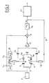
- Fig. 1 is an electrical diagram showing an embodiment of the measuring device according to the invention.
- Fig. 2 is a curve showing the shape of the electrical signal delivered at a characteristic point of the measuring device according to the invention.
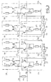
- Fig. 3 is an electrical diagram showing a characteristic detail of the linearization device according to the invention.
- Figs. 4A to 4E are curves illustrating the operating principle of the linearization circuit according to the invention.
- Fig. 5 illustrates an electrical diagram of a characteristic detail of the invention.
- Fig. 1 illustrates an exemplary embodiment of a measuring device adapted to determine the variations in capacity of a variable-type capacitor 1 .
- the capacitor 1 constitutes a capacitive sensor of mechanical quantities, such as force, pressure or acceleration.
- the capacitive sensor is in the form of a cantilever beam, made of a monolithic semiconductor substrate and comprising at least one flexible element of determined thickness, attached to a foot anchor on the substrate.
- the flexible element determines a movable armature of the variable capacitor, the fixed armature of which is formed by a conductive zone formed in the substrate.
- the measuring device aims to detect variations in the capacitance of the capacitor 1 , allowing the delivery of an electrical signal representative of the quantity measured.
- the measuring device comprises an oscillator 2 generating an alternating signal, for example of the square type, of frequency of the order of Megahertz and of amplitude of the order of a few volts.
- the measurement device comprises a detection bridge 3 formed by a first 3 a and a second 3 b branches connected to the oscillator 2 and to ground.
- the first branch 3 a is composed by the capacitor 1 connected in series with a diode 5 with variable capacity.
- the diode 5 is polarized so as to behave like a capacitor whose capacity is able to be controlled by a voltage.
- the anode of the diode 5 is connected, at a common point A , to an armature of the capacitor 1 .
- the second branch 3 b is formed by a capacitor 6 connected in series with a diode 7 with variable capacity identical to the diode 5 .
- the common point B between the capacitor 6 and the anode of the diode 7 , is connected, by means of a DC bias resistor 9 , to a DC bias circuit 10 of the point B and, consequently , of diode 7 , making it possible to fix the balance point of the detection bridge.
- the bias circuit 10 is capable of delivering a reference voltage Vref , preferably adjustable, and formed for example by a divider bridge composed of resistors 7 a , 7 b .
- variable voltage is chosen so that the amplitude of the signal, variable at points A , B , is small compared to that of the reference voltage.
- the capacitor 6 can also constitute a variable capacity sensor, allowing the differential detection of capacities.
- the common points A and B of the first and second branches 3 a , 3 b are connected to the input of a differential stage 12 , via, respectively, a link capacitor 13 , 14 adapted to cut the DC component of the signal from the detection bridge.
- the differential stage 12 is constituted by an amplifier whose non-inverting input is connected to the common point B , while the inverting input is connected to the point A.
- the amplifier 12 is connected to a circuit 15 for synchronous detection of the signal, receiving the synchronization information from the oscillator 2 .
- the synchronous detection circuit 15 produced in a known manner, is connected to a low-pass filter 16 of suitable cut-off frequency, of the order of, for example, 50 Hertz.
- the output of the filter 16 is connected to the common point A of the first branch, by a feedback line 17 in which is mounted a resistor 18 of continuous polarization of the diode 5 .
- the feedback from the detection bridge 3 at the branch which includes the variable capacity, ensures continuous rebalancing of the detection bridge.
- the signal Ve delivered by the filter 16 corresponds to the unbalance signal of the bridge which thus makes it possible to continuously measure the variation in the capacity of the variable capacitor 1 .
- the filter 16 is followed by a circuit 21 for linearization of the signal of imbalance of the bridge Ve , adapted to correct the linearity defect of the sensor 1 and of the diodes 5 and 7 .
- the linearization circuit 21 comprises at least one, and in the example illustrated in FIG. 3 , four differential threshold U1-U4 units, each comprising a first input 22 receiving the imbalance signal Ve and a second input 23 having a reference voltage Vr1 to Vr4 respectively.
- Each unit U1-U4 delivers, respectively, an output current I1-I4 whose law of variation comprises a part with zero slope, connected to a part with determined slope, via an angular point defined for the voltage of corresponding reference.
- At least one, and for example two differential units U1, U2 each deliver an output current I1, I2 whose law of variation comprises a part N with zero slope for a value of the imbalance signal Ve , lower than that of the voltage of reference Vr1, corresponding Vr2 , and a part P with determined slope, for a value of the signal Ve greater than that of the voltage Vr1, Vr2 which corresponds to the angular point of the curve.
- the linearization circuit can also include at least one and, in the example illustrated, two differential units U3, U4 delivering, in accordance with FIGS . 4C-4D , an output signal I3, I4 whose variation law includes a part with zero slope N for a value of the imbalance signal greater than that of the reference voltage Vr3, Vr4, and a part with determined slope P , for a value of the imbalance signal lower than that of the corresponding reference voltage.
- the flat part M of the curve, extending the part with a slope P is not used for the object of the invention.
- Fig. 3 illustrates an embodiment of differential threshold units U unix-U4 capable of delivering an output signal affecting the characteristics set out above.
- Each differential unit U1, U2 comprises a transistor T1 , of the NPN type, the base of which receives the imbalance signal Ve .
- the emitter of transistor T1 differential units U1, U2 is connected, via a resistor 251, 252, to the emitter of an NPN transistor T2.
- the emitter of transistor T2 is connected, via a resistor 26 , to ground, while the collector of this transistor T2 is connected to a bias voltage.
- the base of the transistor T2 of each unit U1, U2 receives the corresponding reference signal Vr1, Vr2 which is delivered, for example, by a voltage divider bridge formed by resistors 27 , 28 , 29 .
- the slope of the current variation curve I1, I2 ( fig. 4A, 4B ) is determined by the value R251- R252 of the corresponding resistance 251, 252 .
- the angular point of this curve is directly defined for the reference voltage Vr1, Vr2 .
- each differential unit U3, U4 comprises a transistor T3 whose base receives the corresponding reference signal Vr3, Vr4 which is delivered, for example, by a divider bridge 30, 31, 32 .
- the emitter of transistor T3 of differential units U un inclusive, U4 is connected to the emitter of a transistor T4 , via a resistor 333, 334 .
- the emitter of transistor T4 is connected to a resistor 35 connected to ground, while the collector of transistor T4 is connected to a bias voltage.
- the base of transistor T4 receives the imbalance signal Ve .
- the slope of the law of variation of the currents I3, I4 can therefore be adapted as a function of the choice of the value R333, R334 of the resistors 333, 334 .
- the angular point of this law is directly determined by the reference voltages Vr3, Vr4 .
- each differential unit U1- U4 is associated with a means 38 for combining the currents I1- I4 coming from the differential units, so as to obtain a resultant current I , image of all the currents delivered by the differential units.
- the combining means 38 each consist of a current mirror and are associated together to add the currents I1 to I4 and obtain a resulting current I , the law of variation of which is illustrated in FIG. 4E .
- each current mirror 38 comprises a PNP type transistor T5 , the collector of which is connected to its base and to the collector of the transistor T1 .
- the emitter of transistor T5 is provided with a bias resistor 41 , while the base of transistor T5 is connected to the base of a transistor T6 whose emitter is connected to a bias resistor 42 .
- the collector of transistor T6 is connected to a collector line 43 connected to the collectors of transistors T6 of the other current mirrors 38 . It should be noted that the choice of resistors 41 , 42 makes it possible to adjust the slope of the law of variation of the currents I1-I4.
- the linearization circuit according to the invention thus makes it possible to ensure linearization of an electrical signal, the law of variation of which exhibits inflections in the opposite direction, as this clearly appears in FIG. 2 .
- the linearization circuit according to the invention may generally comprise n differential units with threshold U , each associated with a combining means 38 .
- the number of differential units is chosen according to the linearization precision to be obtained.
- the type of differential units, used individually or in combination is determined according to the signal to be linearized.
- the linearization, carried out by the circuit can be adjusted by choosing suitable values for the resistances 251, 252, 333, 334, 41 and 42 , as well as for the reference voltages Vr .
- the linearization circuit according to the invention obviously has a limited cost, while presenting the possibility of analog signal adjustment.
- the measurement device as a whole namely the detection bridge and the linearization circuit, is formed from components which can be produced on an integrated circuit.
- the collector of transistor T6 is connected to the collector of a transistor T7 , the emitter of which is connected to ground via a resistor 44 .
- the base of the transistor T7 which is connected to its collector, is connected to the base of a transistor T8 , the emitter of which is connected to ground by means of a resistor 45 .
- the collector of transistor T8 is connected to the collector line 43 from which the currents I1-I4 are subtracted. It should be noted that the slope of the law of variation of the currents can be adapted as a function of the resistances 44 , 45 .
- the invention finds a particularly advantageous application for measuring the variations in capacitance of a capacitor forming a sensor of mechanical quantities, such as force, acceleration or pressure.
Landscapes
- Engineering & Computer Science (AREA)
- Power Engineering (AREA)
- Physics & Mathematics (AREA)
- General Physics & Mathematics (AREA)
- Transmission And Conversion Of Sensor Element Output (AREA)
- Indication And Recording Devices For Special Purposes And Tariff Metering Devices (AREA)
- Measurement Of Resistance Or Impedance (AREA)
- Measuring Fluid Pressure (AREA)
Claims (13)
- Vorrichtung zum Messen der Änderung der Kapazität eines im wesentlichen veränderlichen Kondensators, insbesondere eines Sensors, umfassend:
einen Oszillator (2) zum Erzeugen eines Wechselsignals, eine Meßbrücke (3), umfassend einen ersten (3a) und einen zweiten (3b) Zweig, die mit dem Oszillator verbunden sind, wobei der erste Zweig einen veränderlichen Kondensator (1) umfaßt, der in Reihe mit einem anderen kapazitiven Element (5) geschaltet ist, während der zweite Zweig einen Kondensator (6) umfaßt, der in Reihe mit einem anderen kapazitiven Element (7) geschaltet ist, und eine Differentialstufe (12), deren jeder Eingang mit einem gemeinsamen- Punkt eines Zweiges verbunden ist, der zwischen einem Kondensator und dem entsprechenden kapazitiven Element gelegen ist,
dadurch gekennzeichnet,
daß die kapazitiven Elemente die Dioden mit einer veränderlichen Kapazität (5,7) sind,
daß ein Schaltkreis (10) zum Anlagen einer kontinuierlichen Vorspannung an den gemeinsamen Punkt (B) des zweiten Zweiges vorgesehen ist, um den Gleichgewichtspunkt der Meßbrücke festzulegen,
daß der Differentialstufe (12) Einrichtungen (15,16) zum synchronen Wahrnehmen, die mit dem Oszillator verbunden sind, und Tiefpaßfilter zum Abgeben eines Signals der Gleichgewichtsabweichung (Ve) der Meßbrücke folgen, und daß das Signal der Gleichgewichtsabweichung (Ve) an den gemeinsamen Punkt (A) des ersten Zweiges über eine Rückkoppelungsleitung (17) geleitet wird, um eine kontinuierliche Nachjustierung der Wahrnehmungsbrücke und folglich eine kontinuierliche Messung der Veränderung der Kapazität des veränderlichen Kondensators sicherzustellen. - Vorrichtung nach Anspruch 1,
dadurch gekennzeichnet,
daß jeder Eingang der Differentialstufe (12) mit dem gemeinsamen Punkt eines Zweiges mittels eines Verbindungskondensator (13,14) verbunden ist. - Vorrichtung nach Anspruch 1,
dadurch gekennzeichnet,
daß die gemeinsamen Punkte der Zweige jeweils mit dem Schaltkreis (10) zum Anlegen einer Vorspannung und mit der Rückkopplungsleitung (17) mittels der Widerstände (9,18) zum Anlegen einer Vorspannung an die Dioden mit variabler Kapazität verbunden sind. - Vorrichtung nach Anspruch 1,
dadurch gekennzeichnet,
daß der Tiefpaßfilter mit einem Schaltkreis (21) zum Linearisieren des Nachgleichsignals der Meßbrücke verbunden ist, wobei der Schaltkreis umfaßt:- n Differentialschwelleinheiten (U₁...Un), die jeweils am Eingang das Signal zum Nachgleichen und eine Referenzspannung (Vr) aufnehmen und jeweils am Ausgang einen Strom (I₁...In) abgeben, dessen Verlauf einen Abschnitt (N) mit Steigung Null umfaßt, der mit einem Abschnitt (P) mit vorbestimmter Steigung über einen Eckpunkt verbunden ist, der durch die Referenzspannung begrenzt ist,- und n-Einrichtungen (38) zum Kombinieren der Ströme, die durch die Differentialeinheit abgegeben werden, in der Art, daß ein resultierendes Signal (I) mit vielen Eckpunkten erhalten wird, das, mit dem nachzugleichenden Signal kombiniert, die Linearisierung des letzteren erlaubt. - Vorrichtung nach Anspruch 4,
dadurch gekennzeichnet,
daß wenigstens eine Differentialeinheit einen Ausgangsstrom (I₁, I₂ ...) abgibt, dessen Verlauf einen Abschnitt mit Steigung Null (N) für einen Wert des Signals zum Nachgleichen (Ve) unterhalb der Referenzspannung (Vr) und einen Abschnitt mit vorbestimmter Steigung (P) umfaßt, für einen Wert des Signals zum Nachgleichen (Ve) oberhalb der Referenzspannung. - Vorrichtung nach Anspruch 4 oder 5,
dadurch gekennzeichnet,
daß wenigstens eine Differentialeinheit einen Ausgangsstrom (I₁, I₂ ...) abgibt, dessen Verlauf einen Abschnitt mit Steigung Null (N) für einen Wert des Signals zum Nachgleichen (Ve) oberhalb der Referenzspannung und einen Abschnitt mit vorbestimmter Steigung (P) umfaßt, für einen Wert des Signals zum Nachgleichen (Ve) unterhalb der Referenzspannung (Vr). - Vorrichtung nach Anspruch 5,
dadurch gekennzeichnet,
daß jede Differentialeinheit aus einem ersten Transistor (T₁) ausgebildet ist, umfassend eine Basis, die mit einer Referenzspannung verbunden ist, und einen Emitter, der über einen Widerstand (25₁, 25₂ ...) mit dem Emitter des zweiten Transistors (T₂) verbunden ist, dessen Basis das Signal zum Nachgleichen (Ve) aufnimmt, während der Kollektor den Ausgangsstrom (I₁, I₂ ...) abgibt. - Vorrichtung nach Anspruch 6,
dadurch gekennzeichnet,
daß jede Differentialeinheit durch einen ersten Transistor (T₃) ausgebildet ist, umfassend eine Basis zum Aufnehmen des Signals zum Nachgleichen, und einen Emitter, der über einen Widerstand (33₃, 33₄ ...) mit dem Emitter eines zweiten Transistors (T₄) verbunden ist, an dessen Basis die Referenzspannung anliegt, während der Kollektor den Ausgangsstrom (I₃, I₄ ...) abgibt. - Vorrichtung nach Anspruch 7 oder 8,
dadurch gekennzeichnet,
daß die Widerstände des Emitters (25₁, 25₂ ..., 33₃, 33₄ ..., 41, 42) die Steigung (P) des Verlaufs der Änderung des Ausgangsstroms der Analogeinheiten bestimmen. - Vorrichtung nach Anspruch 4,
dadurch gekennzeichnet,
daß jede Einrichtung (38) zum Kombinieren durch einen Stromspiegel ausgebildet ist. - Vorrichtung nach Anspruch 10,
dadurch gekennzeichnet,
daß die Stromspiegel (38) eine Subtraktion des Ausgangsstroms sicherstellen, der durch die Analogeinheiten abgegeben wird. - Vorrichtung nach Anspruch 10,
dadurch gekennzeichnet,
daß die Stromspiegel (38) eine Addition der Ausgangsströme sicherstellen, die durch die Analogeinheiten abgegeben werden. - Vorrichtung nach Anspruch 1, dadurch gekennzeichnet, daß der Kondensator (6) des zweiten Zweiges von einer veränderlichen Art und Weise ist, um eine Differentialmessung der Kapazitäten sicherzustellen.
Applications Claiming Priority (3)
| Application Number | Priority Date | Filing Date | Title |
|---|---|---|---|
| FR8917551 | 1989-12-29 | ||
| FR8917551A FR2656698B1 (fr) | 1989-12-29 | 1989-12-29 | Dispositif de mesure des variations de la capacite d'un condensateur formant, notamment, un capteur. |
| PCT/FR1990/000961 WO1991009812A2 (fr) | 1989-12-29 | 1990-12-28 | Dispositif de mesure des variations de la capacite d'un condensateur formant, notamment, un capteur |
Publications (2)
| Publication Number | Publication Date |
|---|---|
| EP0510061A1 EP0510061A1 (de) | 1992-10-28 |
| EP0510061B1 true EP0510061B1 (de) | 1994-04-20 |
Family
ID=9389226
Family Applications (1)
| Application Number | Title | Priority Date | Filing Date |
|---|---|---|---|
| EP91902297A Expired - Lifetime EP0510061B1 (de) | 1989-12-29 | 1991-07-25 | Vorrichtung zur messung der änderung der kapazität eines kondensators, insbesondere eines sensors |
Country Status (6)
| Country | Link |
|---|---|
| US (1) | US5311140A (de) |
| EP (1) | EP0510061B1 (de) |
| DE (1) | DE69008363T2 (de) |
| ES (1) | ES2051118T3 (de) |
| FR (1) | FR2656698B1 (de) |
| WO (1) | WO1991009812A2 (de) |
Families Citing this family (22)
| Publication number | Priority date | Publication date | Assignee | Title |
|---|---|---|---|---|
| JP3139305B2 (ja) * | 1994-08-24 | 2001-02-26 | 株式会社村田製作所 | 容量型加速度センサ |
| AT401826B (de) * | 1995-06-01 | 1996-12-27 | Peter Ing Klementschitz | Messverfahren |
| US5659195A (en) * | 1995-06-08 | 1997-08-19 | The Regents Of The University Of California | CMOS integrated microsensor with a precision measurement circuit |
| DE19528384C2 (de) * | 1995-08-02 | 1999-09-30 | Ulrich Pok | Kapazitive Meßeinrichtung zur kontinuierlichen Standregelung für Medien unterschiedlicher Dielektrizitätskonstanten |
| US5808198A (en) * | 1997-05-19 | 1998-09-15 | The Charles Stark Draper Laboratory, Inc. | RF balanced capacitive vibration sensor system |
| US20040099061A1 (en) | 1997-12-22 | 2004-05-27 | Mks Instruments | Pressure sensor for detecting small pressure differences and low pressures |
| US6366099B1 (en) | 1999-12-21 | 2002-04-02 | Conrad Technologies, Inc. | Differential capacitance sampler |
| US6622092B1 (en) * | 2000-03-31 | 2003-09-16 | The United States Of America As Represented By The Secretary Of The Navy | Predictor for optimal broadband impedance matching |
| US7194390B1 (en) * | 2000-03-31 | 2007-03-20 | United States Of America As Represented By The Secretary Of The Navy | Predictor of minimal noise figure for wideband amplifier |
| FR2818676B1 (fr) * | 2000-12-27 | 2003-03-07 | Freyssinet Int Stup | Procede de demontage d'un cable de precontrainte et dispositif pour la mise en oeuvre |
| US20030121332A1 (en) * | 2001-12-21 | 2003-07-03 | Mathew Santhi E. | Pressure transducer with dual slope output |
| US6993973B2 (en) * | 2003-05-16 | 2006-02-07 | Mks Instruments, Inc. | Contaminant deposition control baffle for a capacitive pressure transducer |
| US7327275B2 (en) | 2004-02-02 | 2008-02-05 | Gecko Alliance Group Inc. | Bathing system controller having abnormal operational condition identification capabilities |
| US7201057B2 (en) * | 2004-09-30 | 2007-04-10 | Mks Instruments, Inc. | High-temperature reduced size manometer |
| US7141447B2 (en) * | 2004-10-07 | 2006-11-28 | Mks Instruments, Inc. | Method of forming a seal between a housing and a diaphragm of a capacitance sensor |
| US7137301B2 (en) * | 2004-10-07 | 2006-11-21 | Mks Instruments, Inc. | Method and apparatus for forming a reference pressure within a chamber of a capacitance sensor |
| US7204150B2 (en) | 2005-01-14 | 2007-04-17 | Mks Instruments, Inc. | Turbo sump for use with capacitive pressure sensor |
| US7368923B2 (en) * | 2005-12-22 | 2008-05-06 | Honeywell International Inc. | Time interval trimmed differential capacitance sensor |
| US9063067B1 (en) | 2010-11-17 | 2015-06-23 | Alvin P. Schmitt | Moisture sensing devices |
| EP3074763A1 (de) | 2013-11-25 | 2016-10-05 | Oil States Industries, Inc. | Verfahren und system zur integritätsüberwachung von elastomeren flexiblen kompositelementen |
| GB2615799A (en) | 2022-02-18 | 2023-08-23 | Weiner Nicholas | Impedance sensor |
| US12474386B2 (en) | 2022-02-18 | 2025-11-18 | Nicholas Weiner | Impedance measurement |
Family Cites Families (5)
| Publication number | Priority date | Publication date | Assignee | Title |
|---|---|---|---|---|
| FR2337346A1 (fr) * | 1975-12-30 | 1977-07-29 | Onera (Off Nat Aerospatiale) | Pont de mesure de capacites |
| US4241303A (en) * | 1979-01-17 | 1980-12-23 | The Babcock & Wilcox Company | Linearization circuit |
| US4673869A (en) * | 1985-02-13 | 1987-06-16 | Phillips Petroleum Company | Dielectric constant detector capacitance matching |
| US4684886A (en) * | 1985-05-17 | 1987-08-04 | Doyle James H | Automatic equalizer |
| JPS62168408A (ja) * | 1985-11-21 | 1987-07-24 | Shimadzu Corp | Mri装置用アンテナ回路自動共振・整合装置 |
-
1989
- 1989-12-29 FR FR8917551A patent/FR2656698B1/fr not_active Expired - Fee Related
-
1990
- 1990-12-28 US US07/924,049 patent/US5311140A/en not_active Expired - Fee Related
- 1990-12-28 DE DE69008363T patent/DE69008363T2/de not_active Expired - Fee Related
- 1990-12-28 ES ES91902297T patent/ES2051118T3/es not_active Expired - Lifetime
- 1990-12-28 WO PCT/FR1990/000961 patent/WO1991009812A2/fr not_active Ceased
-
1991
- 1991-07-25 EP EP91902297A patent/EP0510061B1/de not_active Expired - Lifetime
Non-Patent Citations (2)
| Title |
|---|
| IEEE Transactions on Instrumentation and Measurement, Vol. 21, No. 1, Fevrier 1972, New York US, J.E. Sigdell: "A principle for capacitance measurement, suitable for linear evaluation of capacitance transducers", pages 60-61 * |
| PATENT ABSTRACTS OF JAPAN, Vol. 12, No. 7 (E-571), 9 janvier 1988, & JP-A-6 216 84 08 * |
Also Published As
| Publication number | Publication date |
|---|---|
| DE69008363T2 (de) | 1994-11-17 |
| ES2051118T3 (es) | 1994-06-01 |
| WO1991009812A2 (fr) | 1991-07-11 |
| DE69008363D1 (de) | 1994-05-26 |
| WO1991009812A3 (fr) | 1991-08-22 |
| US5311140A (en) | 1994-05-10 |
| EP0510061A1 (de) | 1992-10-28 |
| FR2656698B1 (fr) | 1992-05-07 |
| FR2656698A1 (fr) | 1991-07-05 |
Similar Documents
| Publication | Publication Date | Title |
|---|---|---|
| EP0510061B1 (de) | Vorrichtung zur messung der änderung der kapazität eines kondensators, insbesondere eines sensors | |
| EP0285478B1 (de) | Konvertierschaltung von analogen auf digitale Signale | |
| EP2541213B1 (de) | Verfahren zur Reduzierung der Nichtlinearität beim Messen eines physikalischen Parameters, und elektronischer Schaltkreis zu dessen Umsetzung | |
| CA2831353C (fr) | Procede et systeme de detection d'un court-circuit affectant un capteur | |
| EP2726832B1 (de) | Resistive vorrichtung mit einem silicium-nanodraht-dehnungsmessstreifen und verfahren zur optimierung des stromverbrauchs einer solchen vorrichtung | |
| CH628993A5 (fr) | Appareil de detection d'un champ magnetique exterieur. | |
| EP2887014A1 (de) | Elektronischer Schaltkreis zur Drehgeschwindigkeitsmessung in einem MEMS Kreisel und Verfahren zu seiner Ausführung | |
| WO2012156016A1 (fr) | Mesure differentielle de tension | |
| EP0990128B1 (de) | Druckwandler mit kompensation der nichtlinearität der nulldrift für tiefe temperaturen | |
| EP2662667A1 (de) | Verfahren zum Messen eines physikalischen Parameters, und elektronischer Schnittstellenschaltkreis eines kapazitives Sensors zu dessen Umsetzung | |
| EP0227861B1 (de) | Verfahren zum Messen einer physikalischen Grösse mit numerischen Daten unter Verwendung einer analogen Messvorrichtung und Messapparat für dieses Verfahren | |
| EP2694920B1 (de) | Verfahren zum korrigieren der messung der spannung an den anschlüssen eines sensors | |
| FR2764068A1 (fr) | Circuit pour mesurer le courant dans les electrodes d'un capteur de gaz en ceramique | |
| FR2496894A1 (fr) | Circuit de commande d'un accelerometre electrostatique | |
| EP0796421B1 (de) | Filtervorrichtung, insbesondere für die kraftstoffanzeige in automobilen | |
| EP0266282B1 (de) | Lagealarmanlage | |
| FR2656699A1 (fr) | Circuit analogique de linearisation. | |
| FR2473183A1 (fr) | Montage de circuit servant a convertir une variation de resistance en une variation de frequence | |
| EP1691203B1 (de) | Elektronische Schaltung mit rauscharmem Messkondensator sowie mit einer solchen Schaltung ausgerüsteter Beschleunigungsaufnehmer | |
| FR2908508A1 (fr) | Dispositif electronique, destine a realiser la mesure et la detection de variations d'une grandeur physique a mesurer | |
| FR2796725A1 (fr) | Dispositif de mesure de la sensibilite d'un capteur de champ magnetique a effet hall | |
| FR2659447A1 (fr) | Dispositif de mesure de force comprenant un transducteur piezoresistif compense en temperature. | |
| FR2852398A1 (fr) | Systeme de mesure d'un champ magnetique basse frequence et systeme de modukation d'un champ magnetique mis en oeuvre dans le systeme de mesure | |
| FR2565353A1 (fr) | Procede pour mesurer des capacites, notamment de faibles capacites, dans lequel on utilise deux capacites de reference | |
| EP0924525B1 (de) | Verfahren zur Einstellung einer eine kapazitive Grösse in eine korrespondierende Spannung umsetzende Signalverarbeitungsschaltung |
Legal Events
| Date | Code | Title | Description |
|---|---|---|---|
| PUAI | Public reference made under article 153(3) epc to a published international application that has entered the european phase |
Free format text: ORIGINAL CODE: 0009012 |
|
| 17P | Request for examination filed |
Effective date: 19920710 |
|
| AK | Designated contracting states |
Kind code of ref document: A1 Designated state(s): BE CH DE ES GB IT LI NL SE |
|
| 17Q | First examination report despatched |
Effective date: 19921120 |
|
| RAP1 | Party data changed (applicant data changed or rights of an application transferred) |
Owner name: SOCIETE D'APPLICATIONS GENERALES D'ELECTRICITE ET |
|
| GRAA | (expected) grant |
Free format text: ORIGINAL CODE: 0009210 |
|
| AK | Designated contracting states |
Kind code of ref document: B1 Designated state(s): BE CH DE ES GB IT LI NL SE |
|
| REF | Corresponds to: |
Ref document number: 69008363 Country of ref document: DE Date of ref document: 19940526 |
|
| REG | Reference to a national code |
Ref country code: ES Ref legal event code: FG2A Ref document number: 2051118 Country of ref document: ES Kind code of ref document: T3 |
|
| GBT | Gb: translation of ep patent filed (gb section 77(6)(a)/1977) |
Effective date: 19940505 |
|
| ITF | It: translation for a ep patent filed | ||
| EAL | Se: european patent in force in sweden |
Ref document number: 91902297.0 |
|
| PLBE | No opposition filed within time limit |
Free format text: ORIGINAL CODE: 0009261 |
|
| STAA | Information on the status of an ep patent application or granted ep patent |
Free format text: STATUS: NO OPPOSITION FILED WITHIN TIME LIMIT |
|
| 26N | No opposition filed | ||
| PGFP | Annual fee paid to national office [announced via postgrant information from national office to epo] |
Ref country code: NL Payment date: 19951117 Year of fee payment: 6 |
|
| PGFP | Annual fee paid to national office [announced via postgrant information from national office to epo] |
Ref country code: ES Payment date: 19951128 Year of fee payment: 6 |
|
| PGFP | Annual fee paid to national office [announced via postgrant information from national office to epo] |
Ref country code: SE Payment date: 19951218 Year of fee payment: 6 |
|
| PGFP | Annual fee paid to national office [announced via postgrant information from national office to epo] |
Ref country code: GB Payment date: 19951222 Year of fee payment: 6 |
|
| PGFP | Annual fee paid to national office [announced via postgrant information from national office to epo] |
Ref country code: CH Payment date: 19951227 Year of fee payment: 6 |
|
| PGFP | Annual fee paid to national office [announced via postgrant information from national office to epo] |
Ref country code: BE Payment date: 19960117 Year of fee payment: 6 |
|
| PGFP | Annual fee paid to national office [announced via postgrant information from national office to epo] |
Ref country code: DE Payment date: 19960129 Year of fee payment: 6 |
|
| PG25 | Lapsed in a contracting state [announced via postgrant information from national office to epo] |
Ref country code: GB Effective date: 19961228 |
|
| PG25 | Lapsed in a contracting state [announced via postgrant information from national office to epo] |
Ref country code: SE Effective date: 19961229 |
|
| PG25 | Lapsed in a contracting state [announced via postgrant information from national office to epo] |
Ref country code: ES Free format text: LAPSE BECAUSE OF EXPIRATION OF PROTECTION Effective date: 19961230 |
|
| PG25 | Lapsed in a contracting state [announced via postgrant information from national office to epo] |
Ref country code: LI Effective date: 19961231 Ref country code: CH Effective date: 19961231 Ref country code: BE Effective date: 19961231 |
|
| BERE | Be: lapsed |
Owner name: SOC. D'APPLICATIONS GENERALES D'ELECTRICITE ET DE Effective date: 19961231 |
|
| PG25 | Lapsed in a contracting state [announced via postgrant information from national office to epo] |
Ref country code: NL Effective date: 19970701 |
|
| REG | Reference to a national code |
Ref country code: CH Ref legal event code: PL |
|
| GBPC | Gb: european patent ceased through non-payment of renewal fee |
Effective date: 19961228 |
|
| NLV4 | Nl: lapsed or anulled due to non-payment of the annual fee |
Effective date: 19970701 |
|
| PG25 | Lapsed in a contracting state [announced via postgrant information from national office to epo] |
Ref country code: DE Effective date: 19970902 |
|
| EUG | Se: european patent has lapsed |
Ref document number: 91902297.0 |
|
| REG | Reference to a national code |
Ref country code: ES Ref legal event code: FD2A Effective date: 20010201 |
|
| PG25 | Lapsed in a contracting state [announced via postgrant information from national office to epo] |
Ref country code: IT Free format text: LAPSE BECAUSE OF NON-PAYMENT OF DUE FEES;WARNING: LAPSES OF ITALIAN PATENTS WITH EFFECTIVE DATE BEFORE 2007 MAY HAVE OCCURRED AT ANY TIME BEFORE 2007. THE CORRECT EFFECTIVE DATE MAY BE DIFFERENT FROM THE ONE RECORDED. Effective date: 20051228 |