EP0510243A2 - Burstmode Adressenfolgegenerator - Google Patents
Burstmode Adressenfolgegenerator Download PDFInfo
- Publication number
- EP0510243A2 EP0510243A2 EP91110080A EP91110080A EP0510243A2 EP 0510243 A2 EP0510243 A2 EP 0510243A2 EP 91110080 A EP91110080 A EP 91110080A EP 91110080 A EP91110080 A EP 91110080A EP 0510243 A2 EP0510243 A2 EP 0510243A2
- Authority
- EP
- European Patent Office
- Prior art keywords
- address
- signal
- pulse train
- signals
- latched
- Prior art date
- Legal status (The legal status is an assumption and is not a legal conclusion. Google has not performed a legal analysis and makes no representation as to the accuracy of the status listed.)
- Withdrawn
Links
- 230000015654 memory Effects 0.000 claims description 4
- 230000003111 delayed effect Effects 0.000 claims description 2
- 230000005540 biological transmission Effects 0.000 abstract description 6
- 230000003068 static effect Effects 0.000 abstract description 4
- 238000010586 diagram Methods 0.000 description 9
- 230000006870 function Effects 0.000 description 5
- 238000013461 design Methods 0.000 description 2
- 238000000034 method Methods 0.000 description 2
- 238000013459 approach Methods 0.000 description 1
- 238000006243 chemical reaction Methods 0.000 description 1
- 230000008878 coupling Effects 0.000 description 1
- 238000010168 coupling process Methods 0.000 description 1
- 238000005859 coupling reaction Methods 0.000 description 1
- 230000000694 effects Effects 0.000 description 1
- 238000012545 processing Methods 0.000 description 1
- 238000012546 transfer Methods 0.000 description 1
Images


Classifications
-
- G—PHYSICS
- G11—INFORMATION STORAGE
- G11C—STATIC STORES
- G11C8/00—Arrangements for selecting an address in a digital store
- G11C8/04—Arrangements for selecting an address in a digital store using a sequential addressing device, e.g. shift register, counter
Definitions
- a kind of burst address sequence generator (10) is to generate 2 n pulse trains (n is an integer greater than 1) compatible with INTEL 80486 CPU, including the following: One n-bit binary up counter (11), whose input terminal inputs a signal of one first pulse train address (ZERO#) for initializing and to begin counting, and an increment signal (INC) used to trigger the input.
- the output terminal has n count signal C(0, ..., n-1) to couple to n corresponding XOR gates (12); one transparent latch (13), whose input terminal inputs n address bit A(m, ..., m+n-1) signals (in other words, 2 n pulse train burst cycles with size of each transmission data at 2 m bytes; A0 ⁇ A (M-1) as the continuous lowest address of this 2 m bytes); one of the input signals and one latched act signal (ALE), the output is the n latched address signals LA(m, ..., m+n-1), as well as n corresponding XOR gates coupled with the n count signals C(0, ..., n-1) and n latched address signals LA in order to obtain n pulse train address signals SA(m, ..., m+n-1).
- SA can be directly coupled to a static random access memory (SRAM).
- SRAM static random access memory
- This invention also concerns a pulse train burst address sequence generator (20
- the pulse train burst address sequence of a central processing unit (CPU) of the INTEL 80486 is decided by the starting address; the customary technique involves using the clock state machine and based on the value of the starting address to decide the sequence of state transfer.
- the state machine is a programmable array logic (PAL) or a programmable logic device (PLD) to execute, then (n+1)+n register outputs are required as (2 n )+1 states in a state machine and n register outputs for n bits of pulse train addresses.
- PAL programmable array logic
- PLD programmable logic device
- This patent aims to provide a pulse train address sequence generator which can be randomly expanded.
- the generator has the following functions and effects.
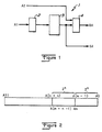
- Fig. 1 is a block diagram of the conventional pulse train address sequence generating device.
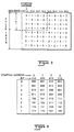
- Fig. 2 is a schematic diagram for the address bits in genrating 2 n pulse train addresses.
- Fig. 3 is a schematic diagram for generally producing the sequence of the pulse train address compatible with the CPU of the INTEL 80486 series.
- Fig. 4 is a schematic diagram for binary state of the starting address based on the identified pulse train sequence of this patent.
- Fig. 5 is a block diagram of the pulse train address sequence generating device based on this patent.
- Fig. 6 is a block diagram explaining the reduction in delay (based on this patent) of the pulse train address sequence generating device.
- Fig. 7 is the timing diagram in coordination with Fig. 6 based on this patent.
- one first address signal (such as column signal) A1 is transmitted to a timing state machine (3) after being latched with a latch device (2) in order to follow a certain sequence to generate the required pulse train address signal (SA).
- SA pulse train address signal
- the address signal can also be transmitted (along with one second address signal, such as row signal) to a multiplexer (4) in order to obtain an address signal (MA) of a dynamic random access memory (DRAM).
- MA address signal
- DRAM dynamic random access memory
- the pulse train address A(m, ..., m+n-1) should follow the sequence determined by the attached table in Fig. 3.
- Each pulse train sequence should be decided only by the first address, that is, the starting address. In the case of 486, the sequence of four pulse trains is the same as the sequence in the left upper corner and in the internal box.
- the working principle of this patent is based on the sequence in the attached table in Fig. 3.
- the starting address is composed of four sets of pulse train address sequences of 0, 1, 2 and 3
- the sequence can be obtained by rewriting in binary form.
- the binary sequence with the starting address as 0 is actually an evolution of a binary up counting.
- one up counting of the binary up counter can be used to tell at what time the phase reversal should occur for various bits in a sequence with a time base.
- bit i of the starting address If the value of the bit i of the starting address is 1, then the value of bit i is just reversed to the value of bit i in the converting and corresponding binary counter in the j pulse train.
- the pulse train burst address sequence generator (10) is used to generate 2 n pulse train address sequences (n is an integer greater than or equal to 1), including the following: one n-bit binary up counter (11), whose input terminal inputs increment signal (INC) used for initializing and to begin counting in order to generate a signal (ZERO#) of the first pulse train address, and an increment signal (INC) for triggering the input.
- n is an integer greater than or equal to 1
- one n-bit binary up counter (11) whose input terminal inputs increment signal (INC) used for initializing and to begin counting in order to generate a signal (ZERO#) of the first pulse train address
- an increment signal (INC) for triggering the input.
- the output terminal is n count signals C(0, 1, ..., n-1) to couple and connect to the n corresponding XOR gates (12); one transparent latch (13), the input terminal inputs one of the n address bits A(m, ..., m+n-1) signals (in other words, the size of each transmitted data is 2 m bytes for 2 n pulse train burst cycles; A1 ⁇ A M-1 is the continuous lowest address of this 2 m bytes) and one latched act signal (ALE).
- ALE latched act signal
- the output is the n latched address signals LA(m, ..., m+n-1), as well as n count signals C(0, 1, ..., n-1) and n latched address signals LA (m, ..., m+n-1) to be coupled to the n corresponding XOR gates.
- A(m, ..., m+n-1) is the starting address; after the transparent latch locks A, A(m, ..., m+n-1) can be randomly varied.
- this transparent latch (13) is not necessary, but can be replaced with A(m, ..., m+n-1) for LA(m, ..., m+n-1) to be directly coupled to the n-th corresponding XOR gate in order to obtain n pulse train address signals SA(m, ..., m+n-1) to be directly coupled to a static random access memory (SRAM) or a multiplexer (14) to become an address signal of the dynamic memory (DRAM).
- SRAM static random access memory
- DRAM dynamic memory
- a module of a dynamic random access memory is used to change Fig. 5 into the circuit as in Fig. 6.
- this is a pulse train sequence generating device (20) capable of reducing the delay in generating the pulse train address, including the following: one delay unit (21) to be used in delay time ⁇ t for the CAS# (CAS# is the signal of capturing the column address for access of data of dynamic RAM); however, ⁇ t > t cah (t cah is the retaining time after changing act at CAS# for the column address); one phase inverter (22) to be used in phase reversal and coupling the delay CAS# to a counter (23) to make an increment for the counter; another input terminal of the counter (23) couples for initializing and to begin counting in order to generate a signal ALE of the first pulse train address; the output terminal is n counting signals C(0, 1, ..., n-1).
- n corresponding latching, multiplexing and XOR gates (24) can be one PAL or one PLD; each input terminal is coupled with a corresponding counting cycle, a corresponding address signal A(m, ..., m+n-1), a corresponding row address RA(0, 1, ..., n-1), and one multiplexer multiplexing selection signal Mux to be used to select the address of the dynamic memory as column or row address.
- ALE address latched act signal
- MA address MA(0, ..., n-1) of the dynamic memory
- the ALE is of high value (or low value)
- the A address signal is locked into a latched signal LA(totalling 0, 1, ..., n-1) in n corresponding LA signals; however, when the LA signal is a low value (or high value), the A address signal is transparent to become MA signal (totalling n corresponding signals (0, 1, ..., n-1)).
- MA(i) Mux ⁇ RA(i)+/Mux ⁇ A(m+i) ⁇ /ALE+/Mux ⁇ [LA(m+1):+:C(i)] ⁇ ALE (3)
- LA(m+i) is the latched address signal A(m+i)
- RA(i) is the corresponding row address
- A(m+i) is the starting address.
- "+” is OR logic
- " ⁇ " is AND logic
- ":+:” is XOR logic
- Mux is the multiplexing selection signal
- /ALE is the phase reverse ALE signal
- /Mux is the phase reversed Mux.
- CS# CYCLE START
- MA MA
Landscapes
- Engineering & Computer Science (AREA)
- Microelectronics & Electronic Packaging (AREA)
- Dram (AREA)
- Bus Control (AREA)
- Memory System (AREA)
Applications Claiming Priority (2)
| Application Number | Priority Date | Filing Date | Title |
|---|---|---|---|
| US689309 | 1991-04-22 | ||
| US07/689,309 US5319759A (en) | 1991-04-22 | 1991-04-22 | Burst address sequence generator |
Publications (2)
| Publication Number | Publication Date |
|---|---|
| EP0510243A2 true EP0510243A2 (de) | 1992-10-28 |
| EP0510243A3 EP0510243A3 (en) | 1993-10-20 |
Family
ID=24767892
Family Applications (1)
| Application Number | Title | Priority Date | Filing Date |
|---|---|---|---|
| EP19910110080 Withdrawn EP0510243A3 (en) | 1991-04-22 | 1991-06-19 | Burst address sequence generator |
Country Status (3)
| Country | Link |
|---|---|
| US (1) | US5319759A (de) |
| EP (1) | EP0510243A3 (de) |
| JP (1) | JPH0830545A (de) |
Cited By (1)
| Publication number | Priority date | Publication date | Assignee | Title |
|---|---|---|---|---|
| EP0840324A3 (de) * | 1993-04-02 | 1998-12-09 | Nec Corporation | Halbleiterspeicher und Zugriffverfahren für solchen Speicher |
Families Citing this family (31)
| Publication number | Priority date | Publication date | Assignee | Title |
|---|---|---|---|---|
| JP3992757B2 (ja) * | 1991-04-23 | 2007-10-17 | テキサス インスツルメンツ インコーポレイテツド | マイクロプロセッサと同期するメモリ、及びデータプロセッサ、同期メモリ、周辺装置とシステムクロックを含むシステム |
| US5638528A (en) * | 1993-11-01 | 1997-06-10 | Motorola, Inc. | Data processing system and a method for cycling longword addresses during a burst bus cycle |
| JP3425811B2 (ja) * | 1994-09-28 | 2003-07-14 | Necエレクトロニクス株式会社 | 半導体メモリ |
| US5491663A (en) * | 1994-11-30 | 1996-02-13 | Sgs-Thomson Microelectronics, Inc. | Pre-charged slave latch with parallel previous state memory |
| US5682354A (en) * | 1995-11-06 | 1997-10-28 | Micron Technology, Inc. | CAS recognition in burst extended data out DRAM |
| US5640364A (en) * | 1994-12-23 | 1997-06-17 | Micron Technology, Inc. | Self-enabling pulse trapping circuit |
| US5675549A (en) * | 1994-12-23 | 1997-10-07 | Micron Technology, Inc. | Burst EDO memory device address counter |
| US5721859A (en) * | 1994-12-23 | 1998-02-24 | Micron Technology, Inc. | Counter control circuit in a burst memory |
| US5610864A (en) | 1994-12-23 | 1997-03-11 | Micron Technology, Inc. | Burst EDO memory device with maximized write cycle timing |
| US5668773A (en) * | 1994-12-23 | 1997-09-16 | Micron Technology, Inc. | Synchronous burst extended data out DRAM |
| US6525971B2 (en) | 1995-06-30 | 2003-02-25 | Micron Technology, Inc. | Distributed write data drivers for burst access memories |
| US5526320A (en) * | 1994-12-23 | 1996-06-11 | Micron Technology Inc. | Burst EDO memory device |
| US5765219A (en) * | 1995-02-23 | 1998-06-09 | Sony Corporation | Apparatus and method for incrementally accessing a system memory |
| KR0171942B1 (ko) * | 1995-06-30 | 1999-03-30 | 김주용 | 버스트 길이 검출 회로 |
| JPH0934827A (ja) * | 1995-07-14 | 1997-02-07 | Canon Inc | メモリ制御装置 |
| US5729504A (en) * | 1995-12-14 | 1998-03-17 | Micron Technology, Inc. | Continuous burst edo memory device |
| US7681005B1 (en) * | 1996-01-11 | 2010-03-16 | Micron Technology, Inc. | Asynchronously-accessible memory device with mode selection circuitry for burst or pipelined operation |
| JPH09231764A (ja) * | 1996-01-19 | 1997-09-05 | Sgs Thomson Microelectron Inc | バーストカウンタ回路及びその動作方法 |
| US5783958A (en) * | 1996-01-19 | 1998-07-21 | Sgs-Thomson Microelectronics, Inc. | Switching master slave circuit |
| US5596616A (en) * | 1996-02-08 | 1997-01-21 | United Microelectronics Corp. | Burst address sequence generator for addressing static random-access-memory devices |
| US6981126B1 (en) * | 1996-07-03 | 2005-12-27 | Micron Technology, Inc. | Continuous interleave burst access |
| US6401186B1 (en) | 1996-07-03 | 2002-06-04 | Micron Technology, Inc. | Continuous burst memory which anticipates a next requested start address |
| US5784331A (en) * | 1996-12-31 | 1998-07-21 | Sgs-Thomson Microelectronics, Inc. | Multiple access memory device |
| US6115321A (en) * | 1997-06-17 | 2000-09-05 | Texas Instruments Incorporated | Synchronous dynamic random access memory with four-bit data prefetch |
| US7103742B1 (en) | 1997-12-03 | 2006-09-05 | Micron Technology, Inc. | Burst/pipelined edo memory device |
| US6480913B1 (en) * | 1998-07-17 | 2002-11-12 | 3Dlabs Inc. Led. | Data sequencer with MUX select input for converting input data stream and to specific output data stream using two exclusive-or logic gates and counter |
| KR100341181B1 (ko) | 1999-11-05 | 2002-06-20 | 윤종용 | 연속적인 읽기 동작을 지원하는 동기형 마스크 롬 장치 |
| JP2005056448A (ja) | 2003-08-01 | 2005-03-03 | Toshiba Corp | 半導体記憶装置 |
| US7927948B2 (en) | 2005-07-20 | 2011-04-19 | Micron Technology, Inc. | Devices with nanocrystals and methods of formation |
| US7972974B2 (en) | 2006-01-10 | 2011-07-05 | Micron Technology, Inc. | Gallium lanthanide oxide films |
| US9646177B2 (en) * | 2011-04-29 | 2017-05-09 | Altera Corporation | Systems and methods for preventing data remanence in memory systems |
Family Cites Families (1)
| Publication number | Priority date | Publication date | Assignee | Title |
|---|---|---|---|---|
| US5126975A (en) * | 1990-10-24 | 1992-06-30 | Integrated Device Technology, Inc. | Integrated cache SRAM memory having synchronous write and burst read |
-
1991
- 1991-04-22 US US07/689,309 patent/US5319759A/en not_active Expired - Lifetime
- 1991-06-19 EP EP19910110080 patent/EP0510243A3/en not_active Withdrawn
- 1991-07-08 JP JP3166956A patent/JPH0830545A/ja active Pending
Non-Patent Citations (2)
| Title |
|---|
| IBM TECHNICAL DISCLOSURE BULLETIN. vol. 33, no. 8, January 1991, NEW YORK US pages 118 - 120 'FAST TTL BURST CONTROLLER FOR MICROPROCESSOR' * |
| IRE WESCON CONVENTION RECORD vol. 34, October 1990, NORTH HOLLYWOOD US pages 29 - 32 AMITAI ET AL. 'BURST MODE MEMORIES IMPROVE CACHE DESIGN' * |
Cited By (1)
| Publication number | Priority date | Publication date | Assignee | Title |
|---|---|---|---|---|
| EP0840324A3 (de) * | 1993-04-02 | 1998-12-09 | Nec Corporation | Halbleiterspeicher und Zugriffverfahren für solchen Speicher |
Also Published As
| Publication number | Publication date |
|---|---|
| EP0510243A3 (en) | 1993-10-20 |
| US5319759A (en) | 1994-06-07 |
| JPH0830545A (ja) | 1996-02-02 |
Similar Documents
| Publication | Publication Date | Title |
|---|---|---|
| EP0510243A2 (de) | Burstmode Adressenfolgegenerator | |
| AU660720B2 (en) | Burst read address generation | |
| US4685089A (en) | High speed, low-power nibble mode circuitry for dynamic memory | |
| US5390149A (en) | System including a data processor, a synchronous dram, a peripheral device, and a system clock | |
| US5699530A (en) | Circular RAM-based first-in/first-out buffer employing interleaved storage locations and cross pointers | |
| EP0136414A2 (de) | Dynamischer Speicher mit schnellem seriellem Modus | |
| EP0561306B1 (de) | Zugriffsverfahren für eine synchrone Halbleiterspeicheranordnung | |
| EP0364110B1 (de) | Halbleiterspeichereinrichtung, die einen Speicher mit Seriengriff aufweist | |
| US4899339A (en) | Digital multiplexer | |
| US5508967A (en) | Line memory | |
| US5398209A (en) | Serial access memory with column address counter and pointers | |
| US5177704A (en) | Matrix transpose memory device | |
| US4694197A (en) | Control signal generator | |
| US4503525A (en) | Common circuit for dynamic memory refresh and system clock function | |
| US5319596A (en) | Semiconductor memory device employing multi-port RAMs | |
| EP0421627A2 (de) | Speichervorrichtung | |
| US6011749A (en) | Integrated circuit having output timing control circuit and method thereof | |
| WO1996021278A1 (en) | Interleaved and sequential counter | |
| EP0743649A2 (de) | Serieller Zugriffspeicher mit reduzierter Kreisverzögerung | |
| KR960032217A (ko) | 듀얼포트 메모리 장치 및 듀얼포트 메모리 장치의 시리얼데이타 출력방법 | |
| CA2045224A1 (en) | Burst address sequence generator | |
| US5291457A (en) | Sequentially accessible non-volatile circuit for storing data | |
| JP2841456B2 (ja) | データ転送方法及びデータバッファ装置 | |
| US4538260A (en) | Electronic time switch | |
| GB2295038A (en) | Test circuit for a semiconductor device |
Legal Events
| Date | Code | Title | Description |
|---|---|---|---|
| PUAI | Public reference made under article 153(3) epc to a published international application that has entered the european phase |
Free format text: ORIGINAL CODE: 0009012 |
|
| AK | Designated contracting states |
Kind code of ref document: A2 Designated state(s): DE GB IT |
|
| PUAL | Search report despatched |
Free format text: ORIGINAL CODE: 0009013 |
|
| AK | Designated contracting states |
Kind code of ref document: A3 Designated state(s): DE GB IT |
|
| 17P | Request for examination filed |
Effective date: 19931214 |
|
| 17Q | First examination report despatched |
Effective date: 19960226 |
|
| STAA | Information on the status of an ep patent application or granted ep patent |
Free format text: STATUS: THE APPLICATION IS DEEMED TO BE WITHDRAWN |
|
| 18D | Application deemed to be withdrawn |
Effective date: 19960709 |