EP0510433A2 - Geschützte Schaltungsstruktur - Google Patents
Geschützte Schaltungsstruktur Download PDFInfo
- Publication number
- EP0510433A2 EP0510433A2 EP92106105A EP92106105A EP0510433A2 EP 0510433 A2 EP0510433 A2 EP 0510433A2 EP 92106105 A EP92106105 A EP 92106105A EP 92106105 A EP92106105 A EP 92106105A EP 0510433 A2 EP0510433 A2 EP 0510433A2
- Authority
- EP
- European Patent Office
- Prior art keywords
- circuit
- substrates
- maintenance
- volatile
- circuit structure
- Prior art date
- Legal status (The legal status is an assumption and is not a legal conclusion. Google has not performed a legal analysis and makes no representation as to the accuracy of the status listed.)
- Withdrawn
Links
Images

Classifications
-
- G—PHYSICS
- G06—COMPUTING OR CALCULATING; COUNTING
- G06F—ELECTRIC DIGITAL DATA PROCESSING
- G06F21/00—Security arrangements for protecting computers, components thereof, programs or data against unauthorised activity
- G06F21/70—Protecting specific internal or peripheral components, in which the protection of a component leads to protection of the entire computer
- G06F21/86—Secure or tamper-resistant housings
-
- G—PHYSICS
- G11—INFORMATION STORAGE
- G11C—STATIC STORES
- G11C8/00—Arrangements for selecting an address in a digital store
- G11C8/20—Address safety or protection circuits, i.e. arrangements for preventing unauthorized or accidental access
-
- H—ELECTRICITY
- H10—SEMICONDUCTOR DEVICES; ELECTRIC SOLID-STATE DEVICES NOT OTHERWISE PROVIDED FOR
- H10W—GENERIC PACKAGES, INTERCONNECTIONS, CONNECTORS OR OTHER CONSTRUCTIONAL DETAILS OF DEVICES COVERED BY CLASS H10
- H10W42/00—Arrangements for protection of devices
-
- H—ELECTRICITY
- H10—SEMICONDUCTOR DEVICES; ELECTRIC SOLID-STATE DEVICES NOT OTHERWISE PROVIDED FOR
- H10W—GENERIC PACKAGES, INTERCONNECTIONS, CONNECTORS OR OTHER CONSTRUCTIONAL DETAILS OF DEVICES COVERED BY CLASS H10
- H10W42/00—Arrangements for protection of devices
- H10W42/40—Arrangements for protection of devices protecting against tampering, e.g. unauthorised inspection or reverse engineering
- H10W42/405—Arrangements for protection of devices protecting against tampering, e.g. unauthorised inspection or reverse engineering using active circuits
-
- G—PHYSICS
- G06—COMPUTING OR CALCULATING; COUNTING
- G06F—ELECTRIC DIGITAL DATA PROCESSING
- G06F2221/00—Indexing scheme relating to security arrangements for protecting computers, components thereof, programs or data against unauthorised activity
- G06F2221/21—Indexing scheme relating to G06F21/00 and subgroups addressing additional information or applications relating to security arrangements for protecting computers, components thereof, programs or data against unauthorised activity
- G06F2221/2143—Clearing memory, e.g. to prevent the data from being stolen
-
- H—ELECTRICITY
- H10—SEMICONDUCTOR DEVICES; ELECTRIC SOLID-STATE DEVICES NOT OTHERWISE PROVIDED FOR
- H10W—GENERIC PACKAGES, INTERCONNECTIONS, CONNECTORS OR OTHER CONSTRUCTIONAL DETAILS OF DEVICES COVERED BY CLASS H10
- H10W72/00—Interconnections or connectors in packages
- H10W72/071—Connecting or disconnecting
- H10W72/072—Connecting or disconnecting of bump connectors
- H10W72/07251—Connecting or disconnecting of bump connectors characterised by changes in properties of the bump connectors during connecting
-
- H—ELECTRICITY
- H10—SEMICONDUCTOR DEVICES; ELECTRIC SOLID-STATE DEVICES NOT OTHERWISE PROVIDED FOR
- H10W—GENERIC PACKAGES, INTERCONNECTIONS, CONNECTORS OR OTHER CONSTRUCTIONAL DETAILS OF DEVICES COVERED BY CLASS H10
- H10W72/00—Interconnections or connectors in packages
- H10W72/20—Bump connectors, e.g. solder bumps or copper pillars; Dummy bumps; Thermal bumps
- H10W72/251—Materials
- H10W72/252—Materials comprising solid metals or solid metalloids, e.g. PbSn, Ag or Cu
Definitions
- This invention relates to the protection of electrical circuitry from reverse engineering, and more particularly to the protection of access codes embedded within integrated circuitry.
- circuitry It is very important to prevent unauthorized access to certain portions of electrical circuits, particularly integrated circuits. For example, digital codes or other data may be stored in certain portions of the circuit to prevent its unauthorized use; the circuit will function properly only if the user enters the appropriate code.
- circuitry may be compromised, however, by various methods of analysis, such as visual inspection, microprobing, secondary electron emission voltage-contrast analysis, etc. A number of techniques have been used in the past to prevent such reverse engineering.
- 4,766,516 also discloses a use control scheme for a secure system which has circuitry on several printed circuit boards. Each circuit transmits a control code to enable the circuitry on the next board in order when it itself has received its control code; an external software verification unit transmits the control code for the first board. Overall system operation is disabled if any of the boards are tampered with or missing.
- the present invention seeks to provide a circuit structure that is more secure than prior circuits, and disables itself when access is attempted so that it cannot be reverse engineered.
- the circuit structure includes a pair of opposed substrates, with a volatile circuit fabricated on at least one of the substrates so that it faces the other substrate.
- the substrates are held in a fixed position with respect to each other, with the volatile circuit maintained by a maintenance circuit that extends between the substrates. Moving the substrates with respect to each other interrupts the maintenance circuit, thereby altering the volatile circuit so that it cannot be successfully reversed engineered.
- the maintenance circuit includes several pairs of opposed conductive indium bumps that extend from the opposed substrates to contact each other and establish both a mechanical bond and an electrical path for the maintenance circuit.
- This circuit extends in multiple traverses back and forth between the substrates, through the bumps.
- the volatile circuit may be divided into portions located on each of the substrates, in which case the maintenance circuit can also interconnect the divided portions.
- Opposed peripheral dams may also be provided on the substrates to impede access to the interior of the circuit structure. The dams may be connected such that open circuiting a pair of opposed dams or short circuiting adjacent dams also interrupts the maintenance circuit.
- the volatile circuit is preferably implemented as a volatile memory, with a power supply circuit for the memory serving as the maintenance circuit. Moving the substrates relative to each other breaks the power supply circuit, causing the memory information to erase in the case of a static memory, or to decay for a dynamic memory. In either case, a secure code originally written into the memory is altered so that reverse engineering the memory will not yield the original code.
- the present invention takes a direct departure from the prior approach of trying to protect a secure circuit by preventing physical access to the circuit.
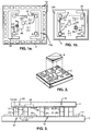
- FIGS. 1a and 1b A somewhat simplified circuit structure that illustrates the principles of the invention is shown in FIGS. 1a and 1b.
- the circuit structure is formed from a pair of substrates 2 and 4, prepared from a suitable semiconductor material such as silicon. When assembled, substrate 4 is "flip-chip" mounted to substrate 2 as illustrated in FIG. 2, with the circuits on each substrate facing each other.
- a circuit 6a to be secured is fabricated on substrate 2.
- the entire circuit may be formed on substrate 2, or it may be divided into two portions, with one portion 6a on substrate 2 and the other portion 6b on substrate 4.
- the secure circuit is preferably implemented as a volatile digital memory, such as a static or dynamic RAM (random access memory).
- Dynamic RAM cells use a transistor and capacitor combination, with the digital information represented by a charge stored on each of the capacitors in the memory array.
- a static RAM uses a series of transistors to form a flip-flop for each cell in the array. Both types of memory are considered "volatile" in the sense that they must be constantly maintained to retain their memory codes. The maintenance function is performed by a power supply. If a dynamic RAM is not replenished with a refresh signal (typically every two ms), as well as supplied with a power supply signal, the capacitors will lose their charge and the code will be altered. If power is removed from a static memory, the flip-flop will reset and the memory will display a different code when power is restored.
- a refresh signal typically every two ms
- the secure circuit 6a, 6b will generally be part of a larger overall circuit, indicated by hash lines 8.
- Substrate 2 is larger than substrate 4, and includes a series of conductive contact pads 10 around its periphery for electrically communicating with a circuit board. At least one conductive "bump" 12, and preferably a plurality of such bumps, are formed on the opposed faces of the two substrates in alignment with each other. Substrate 4 is emplaced over substrate 2 so that the opposed conductive bumps on the two substrates mate with each other, providing electrical connections between the substrates and also a mechanical engagement that bonds the substrates in place and prevents them from moving with respect to each other. Conductive bump technology is known in the art, and is described, for example, in earlier European Patent Application Publ. No. 444 469 (Art. 54 (3) EPC).
- the conductive bumps are preferably formed from indium.
- indium has a lower melting temperature than most adhesive bonds and is attacked by acids, so that if access to the secure circuit is attempted by chemical melting through one of the substrates, the electrical connection provided by the indium contacts will be broken. As explained below, this will cause the secure code stored in the memory circuit to be altered, so that even if it is reversed engineered, the wrong code will be discovered.
- Solder bumps could be used instead of indium bumps. With solder bumps, however, the spacing between the substrates would be about 25 microns, as opposed to about 4-6 microns for indium bumps. Solder bumps thus leave more clearance between the substrates for inserting a probe to access the secure circuitry.
- the bumps might also be formed from other conductive materials such as gold or conductive adhesive.
- a power supply circuit for the volatile memory 6a, 6b includes a number of conductive bumps pairs that are connected in series as part of the power supply circuit. Separating or otherwise moving the substrates with respect to each other to gain access to the secure circuitry requires that these pairs be broken. In this event the power supply circuit is interrupted and the volatile memory which it serves changes state, thus rendering harmless any access to the secure circuit after it has been exposed.
- the refresh circuit rather than the power supply circuit might be interrupted by moving the substrates relative to each other to implement the memory change of state.
- opposed conductive dams 14a and 14b may be formed on substrates 2 and 4, respectively, around the internal circuitry.
- the conductive dam 14b on substrate 4 is located in the peripheral region of that substrate, while the conductive 14a dam on substrate 2 is located inward of the contact pads 10.
- the conductive dams are fabricated in a manner similar to the conductive bumps, and will generally be of the same material. They physically impede lateral access to the internal circuitry, and may be connected in series with the conductive bumps as part of the maintenance circuit. Separating the substrates thus also separates the mating dams, again open circuiting the power supply circuit.
- the dams on each substrate may be divided into separate segments, with one of the segments included in the power supply circuit and the other segment maintained at a different voltage level.
- the power supply circuit may make only a single traverse between one substrate and the other, the circuit structure is preferably fabricated so that it makes multiple traverses, thereby providing assurance that it will be interrupted if the structure is tampered with.
- FIGs. 1a, 1b and 3 Such an arrangement is illustrated in FIGs. 1a, 1b and 3.
- the power supply circuit is indicated in dashed lines just below the opposed surfaces of the two substrates, although in practice it would be implemented by a metallization pattern on the surfaces themselves.
- memory circuits 6a and 6b are shown on the substrate surfaces, while in practice they would be embedded within the substrates.
- An external power supply such as a battery is connected to the circuit structure described thus far at one of the contact pads P on substrate 2.
- An electrical connection is made between contact pad P and one of the conductive bumps A1 on the same substrate by extending under the adjacent dam if present with a dielectric layer separating the two.
- the circuit continues from bump A1 on substrate 2 to the aligned bump A2 on substrate 4.
- the convention used for these figures is that, for an aligned pair of conductive bumps or dams, the bump or dam on the power supply side is indicated by the numeral "1", while the opposed bump or dam on the secure circuit side is indicated by the numeral "2".
- an electrical connection on one substrate is indicated by a solid line, while the image of that connection on the opposed substrate is indicated by a dashed line.
- the power supply circuit it extends in succession from bump A2 to bump B1 via lead 16 on substrate 4; from bump B1 to bump B2 on substrate 2; from bump B2 to bump C1 on substrate 2 via lead 18; from bump C1 to bump C2 on substrate 4; from bump C2 to dam D1 via lead 20 on substrate 4; from dam D1 on substrate 4 to dam D2 on substrate 2; from dam D2 to bump E1 via lead 22 on substrate 2; and finally from bump E1 to memory circuit 6a via lead 24 on substrate 2 and to memory 6b via bump E2 and lead 26 on substrate 4.
- Signal connections between the two segments of the memory circuit are provided along lead 28 (substrate 2) and lead 30 (substrate 4) via bumps F1 and F2.
- the two substrates may be encapsulated by conventional techniques if desired, with the wire bonding pads around the periphery of substrate 2 left exposed.
- the completed circuit package 32 can then be mounted to a printed circuit board 34 that includes a power supply such as a battery 36.
- An opening 38 is formed in the printed circuit board just larger than the outer dimensions of substrate 4, so that the secure circuit package 32 can be mounted to the board with the substrate 4 fitting in opening 38.
- a series of wire bonding pads 40 on the board around the periphery of opening 38 mate with pads 10 on the larger substrate 2.
- the battery 36 is connected via lead 42 on the circuit board to a board pad P' that mates with power supply pad P on the substrate 2.
- the assembly may then be encapsulated within encapsulation layers 44 by conventional techniques, with external contact pads 46 along the periphery of the circuit board 44 left exposed.
- the assembly may also be packaged separately, independent of an integrated circuit board, using conventional integrated circuit packaging techniques.
Landscapes
- Engineering & Computer Science (AREA)
- Computer Security & Cryptography (AREA)
- Computer Hardware Design (AREA)
- Theoretical Computer Science (AREA)
- Microelectronics & Electronic Packaging (AREA)
- Software Systems (AREA)
- Physics & Mathematics (AREA)
- General Engineering & Computer Science (AREA)
- General Physics & Mathematics (AREA)
- Storage Device Security (AREA)
- Semiconductor Integrated Circuits (AREA)
- Combinations Of Printed Boards (AREA)
Applications Claiming Priority (2)
| Application Number | Priority Date | Filing Date | Title |
|---|---|---|---|
| US07/692,334 US5072331A (en) | 1991-04-26 | 1991-04-26 | Secure circuit structure |
| US692334 | 1991-04-26 |
Publications (2)
| Publication Number | Publication Date |
|---|---|
| EP0510433A2 true EP0510433A2 (de) | 1992-10-28 |
| EP0510433A3 EP0510433A3 (en) | 1993-08-25 |
Family
ID=24780152
Family Applications (1)
| Application Number | Title | Priority Date | Filing Date |
|---|---|---|---|
| EP19920106105 Withdrawn EP0510433A3 (en) | 1991-04-26 | 1992-04-09 | Secure circuit structure |
Country Status (3)
| Country | Link |
|---|---|
| US (1) | US5072331A (de) |
| EP (1) | EP0510433A3 (de) |
| JP (1) | JPH05158799A (de) |
Cited By (16)
| Publication number | Priority date | Publication date | Assignee | Title |
|---|---|---|---|---|
| WO1996034410A1 (de) * | 1995-04-25 | 1996-10-31 | Siemens Aktiengesellschaft | Chip-abdeckung |
| WO1996034411A1 (de) * | 1995-04-25 | 1996-10-31 | Siemens Aktiengesellschaft | Chip-abdeckung |
| WO1996034409A1 (de) * | 1995-04-25 | 1996-10-31 | Siemens Aktiengesellschaft | Chip-abdeckung |
| FR2746962A1 (fr) * | 1996-04-01 | 1997-10-03 | Schlumberger Ind Sa | Dispositif de securite d'une pastille semi-conductrice |
| US5883429A (en) * | 1995-04-25 | 1999-03-16 | Siemens Aktiengesellschaft | Chip cover |
| WO1999016131A1 (de) * | 1997-09-19 | 1999-04-01 | Fraunhofer-Gesellschaft zur Förderung der angewandten Forschung e.V. | Verdrahtungsverfahren für halbleiter-bauelemente zur verhinderung von produktpiraterie und produktmanipulation, durch das verfahren hergestelltes halbleiter-bauelement und verwendung des halbleiter-bauelements in einer chipkarte |
| EP0860881A3 (de) * | 1997-02-24 | 1999-08-18 | General Instrument Corporation | Gegen unbefugte Handhabung gesicherte integrierte Schaltung |
| EP0860882A3 (de) * | 1997-02-24 | 1999-08-18 | General Instrument Corporation | Bonddrahtabschirmung für integrierte Schaltung zum Schutz gegen unbefugte Handhabung |
| WO2000067319A1 (de) * | 1999-05-03 | 2000-11-09 | Infineon Technologies Ag | Verfahren und vorrichtung zur sicherung eines mehrdimensional aufgebauten chipstapels |
| GB2323212B (en) * | 1995-12-20 | 2000-12-13 | Intel Corp | Secure semiconductor device |
| EP1365305A1 (de) * | 2002-05-13 | 2003-11-26 | Sagem S.A. | Eindringgeschütztes Gehäuse mit Widerstandsmaschennetzwerk |
| WO2003067604A3 (de) * | 2002-02-08 | 2003-12-11 | Conti Temic Microelectronic | Schaltungsanordnung mit einer mit einem programmierbaren speicherelement bestückten leiterplatte |
| FR2841197A1 (fr) * | 2002-05-11 | 2003-12-26 | Bosch Gmbh Robert | Dispositif de commande pour un vehicule automobile |
| EP1564676A3 (de) * | 1997-02-13 | 2006-01-18 | Micron Technology, Inc. | Betrugssichere Chipkarte und Verfahren zum Schutz von Daten einer Chipkarte |
| EP1840964A1 (de) * | 2006-03-31 | 2007-10-03 | Irvine Sensors Corp. | Halbleitervorrichtung mit Zugriffsschutz |
| US8074082B2 (en) | 2004-10-08 | 2011-12-06 | Aprolase Development Co., Llc | Anti-tamper module |
Families Citing this family (21)
| Publication number | Priority date | Publication date | Assignee | Title |
|---|---|---|---|---|
| US5027397A (en) * | 1989-09-12 | 1991-06-25 | International Business Machines Corporation | Data protection by detection of intrusion into electronic assemblies |
| US6782479B1 (en) * | 1991-04-26 | 2004-08-24 | Raytheon Company | Apparatus and method for inhibiting analysis of a secure circuit |
| ATE208918T1 (de) * | 1993-04-28 | 2001-11-15 | Fujitsu Siemens Computers Gmbh | Schutzvorrichtung für schaltungsteile und/oder daten eines elektrotechnischen geräts |
| US5561593A (en) * | 1994-01-27 | 1996-10-01 | Vicon Enterprises, Inc. | Z-interface-board |
| AU6502896A (en) * | 1995-07-20 | 1997-02-18 | Dallas Semiconductor Corporation | Single chip microprocessor, math co-processor, random number generator, real-time clock and ram having a one-wire interface |
| US5856914A (en) * | 1996-07-29 | 1999-01-05 | National Semiconductor Corporation | Micro-electronic assembly including a flip-chip mounted micro-device and method |
| US6075711A (en) * | 1996-10-21 | 2000-06-13 | Alpine Microsystems, Inc. | System and method for routing connections of integrated circuits |
| US6092281A (en) * | 1998-08-28 | 2000-07-25 | Amkor Technology, Inc. | Electromagnetic interference shield driver and method |
| US6707159B1 (en) * | 1999-02-18 | 2004-03-16 | Rohm Co., Ltd. | Semiconductor chip and production process therefor |
| US6160958A (en) * | 1999-06-16 | 2000-12-12 | Eastman Kodak Company | Tamper resistant electronic flash unit for one-time-use camera |
| WO2001015231A1 (fr) * | 1999-08-19 | 2001-03-01 | Seiko Epson Corporation | Panneau de cablage, dispositif semiconducteur, procede de fabrication d'un dispositif semiconducteur, carte a circuit imprime et dispositif electronique |
| CN2388708Y (zh) * | 1999-09-07 | 2000-07-19 | 英属维京群岛盖内蒂克瓦耳有限公司 | 集成电路封装盒结构 |
| US6414884B1 (en) * | 2000-02-04 | 2002-07-02 | Lucent Technologies Inc. | Method and apparatus for securing electronic circuits |
| US7010639B2 (en) * | 2003-06-12 | 2006-03-07 | Hewlett-Packard Development Company, L.P. | Inter integrated circuit bus router for preventing communication to an unauthorized port |
| DE102005005622B4 (de) * | 2005-02-08 | 2008-08-21 | Infineon Technologies Ag | Sicherheits-Chipstapel und ein Verfahren zum Herstellen eines Sicherheits-Chipstapels |
| US8653657B2 (en) * | 2005-08-23 | 2014-02-18 | Rohm Co., Ltd. | Semiconductor chip, method of manufacturing semiconductor chip, and semiconductor device |
| US7880248B1 (en) * | 2005-10-17 | 2011-02-01 | Teledyne Technologies Incorporated | Destructor integrated circuit chip, interposer electronic device and methods |
| US7812428B2 (en) * | 2007-12-05 | 2010-10-12 | Atmel Rousset S.A.S. | Secure connector grid array package |
| US7834442B2 (en) * | 2007-12-12 | 2010-11-16 | International Business Machines Corporation | Electronic package method and structure with cure-melt hierarchy |
| DE102010033662A1 (de) * | 2010-08-06 | 2012-02-09 | Castles Technology Co., Ltd. | Schutzstruktur einer elektronischen Komponente |
| DE102014213375A1 (de) * | 2014-04-23 | 2015-10-29 | Fraunhofer-Gesellschaft zur Förderung der angewandten Forschung e.V. | Mikroelektronisches system mit erhöhter sicherheit vor datenmissbrauch und produktmanipulation und verfahren zur herstellung desselben |
Family Cites Families (9)
| Publication number | Priority date | Publication date | Assignee | Title |
|---|---|---|---|---|
| JPS5599722A (en) * | 1979-01-26 | 1980-07-30 | Hitachi Ltd | Preparation of semiconductor device |
| GB2195478B (en) * | 1986-09-24 | 1990-06-13 | Ncr Co | Security device for sensitive data |
| JPS63124153A (ja) * | 1986-11-05 | 1988-05-27 | インターナシヨナル・ビジネス・マシーンズ・コーポレーシヨン | 記憶情報保護装置 |
| JPS63237144A (ja) * | 1987-03-25 | 1988-10-03 | Sega Enterp:Kk | 模倣防止機能付半導体装置 |
| US4912545A (en) * | 1987-09-16 | 1990-03-27 | Irvine Sensors Corporation | Bonding of aligned conductive bumps on adjacent surfaces |
| US4766516A (en) * | 1987-09-24 | 1988-08-23 | Hughes Aircraft Company | Method and apparatus for securing integrated circuits from unauthorized copying and use |
| US4933898A (en) * | 1989-01-12 | 1990-06-12 | General Instrument Corporation | Secure integrated circuit chip with conductive shield |
| US4982371A (en) * | 1989-05-15 | 1991-01-01 | Dallas Semiconductor Corporation | Compact electronic module having a RAM device |
| US5110299A (en) * | 1990-02-28 | 1992-05-05 | Hughes Aircraft Company | High density interconnect |
-
1991
- 1991-04-26 US US07/692,334 patent/US5072331A/en not_active Expired - Lifetime
-
1992
- 1992-04-09 EP EP19920106105 patent/EP0510433A3/en not_active Withdrawn
- 1992-04-27 JP JP4107815A patent/JPH05158799A/ja active Pending
Cited By (22)
| Publication number | Priority date | Publication date | Assignee | Title |
|---|---|---|---|---|
| WO1996034410A1 (de) * | 1995-04-25 | 1996-10-31 | Siemens Aktiengesellschaft | Chip-abdeckung |
| WO1996034411A1 (de) * | 1995-04-25 | 1996-10-31 | Siemens Aktiengesellschaft | Chip-abdeckung |
| WO1996034409A1 (de) * | 1995-04-25 | 1996-10-31 | Siemens Aktiengesellschaft | Chip-abdeckung |
| KR100407042B1 (ko) * | 1995-04-25 | 2004-02-18 | 지멘스 악티엔게젤샤프트 | 칩커버 |
| RU2164720C2 (ru) * | 1995-04-25 | 2001-03-27 | Сименс Акциенгезелльшафт | Покрытие кристалла интегральной схемы |
| US5883429A (en) * | 1995-04-25 | 1999-03-16 | Siemens Aktiengesellschaft | Chip cover |
| GB2323212B (en) * | 1995-12-20 | 2000-12-13 | Intel Corp | Secure semiconductor device |
| FR2746962A1 (fr) * | 1996-04-01 | 1997-10-03 | Schlumberger Ind Sa | Dispositif de securite d'une pastille semi-conductrice |
| US5881155A (en) * | 1996-04-01 | 1999-03-09 | Schlumberger Industries | Security device for a semiconductor chip |
| EP0800209A1 (de) * | 1996-04-01 | 1997-10-08 | Schlumberger Industries | Schutzanordnung für ein Halbleiterplättchen |
| EP1564676A3 (de) * | 1997-02-13 | 2006-01-18 | Micron Technology, Inc. | Betrugssichere Chipkarte und Verfahren zum Schutz von Daten einer Chipkarte |
| EP0860881A3 (de) * | 1997-02-24 | 1999-08-18 | General Instrument Corporation | Gegen unbefugte Handhabung gesicherte integrierte Schaltung |
| EP0860882A3 (de) * | 1997-02-24 | 1999-08-18 | General Instrument Corporation | Bonddrahtabschirmung für integrierte Schaltung zum Schutz gegen unbefugte Handhabung |
| WO1999016131A1 (de) * | 1997-09-19 | 1999-04-01 | Fraunhofer-Gesellschaft zur Förderung der angewandten Forschung e.V. | Verdrahtungsverfahren für halbleiter-bauelemente zur verhinderung von produktpiraterie und produktmanipulation, durch das verfahren hergestelltes halbleiter-bauelement und verwendung des halbleiter-bauelements in einer chipkarte |
| US6284627B1 (en) | 1997-09-19 | 2001-09-04 | Fraunhofer-Gesellschaft zur Förderung der angewandten Forschung e.V. | Method for wiring semi-conductor components in order to prevent product piracy and manipulation, semi-conductors component made according to this method and use of said semi-conductor component in a chip card |
| WO2000067319A1 (de) * | 1999-05-03 | 2000-11-09 | Infineon Technologies Ag | Verfahren und vorrichtung zur sicherung eines mehrdimensional aufgebauten chipstapels |
| US6853085B2 (en) | 1999-05-03 | 2005-02-08 | Infineon Technologies Ag | Method and device for securing a multi-dimensionally constructed chip stack and chip configuration |
| WO2003067604A3 (de) * | 2002-02-08 | 2003-12-11 | Conti Temic Microelectronic | Schaltungsanordnung mit einer mit einem programmierbaren speicherelement bestückten leiterplatte |
| FR2841197A1 (fr) * | 2002-05-11 | 2003-12-26 | Bosch Gmbh Robert | Dispositif de commande pour un vehicule automobile |
| EP1365305A1 (de) * | 2002-05-13 | 2003-11-26 | Sagem S.A. | Eindringgeschütztes Gehäuse mit Widerstandsmaschennetzwerk |
| US8074082B2 (en) | 2004-10-08 | 2011-12-06 | Aprolase Development Co., Llc | Anti-tamper module |
| EP1840964A1 (de) * | 2006-03-31 | 2007-10-03 | Irvine Sensors Corp. | Halbleitervorrichtung mit Zugriffsschutz |
Also Published As
| Publication number | Publication date |
|---|---|
| JPH05158799A (ja) | 1993-06-25 |
| US5072331A (en) | 1991-12-10 |
| EP0510433A3 (en) | 1993-08-25 |
Similar Documents
| Publication | Publication Date | Title |
|---|---|---|
| US5072331A (en) | Secure circuit structure | |
| US6414884B1 (en) | Method and apparatus for securing electronic circuits | |
| CN101904002B (zh) | 具有球栅阵列网罩的层叠封装安全模块 | |
| US5877547A (en) | Active security device including an electronic memory | |
| US4593384A (en) | Security device for the secure storage of sensitive data | |
| US5389738A (en) | Tamperproof arrangement for an integrated circuit device | |
| EP0860881B1 (de) | Gegen unbefugte Handhabung gesicherte integrierte Schaltung | |
| CN101889344B (zh) | 嵌入式封装防篡改网栅 | |
| US4446475A (en) | Means and method for disabling access to a memory | |
| US5998858A (en) | Microcircuit with memory that is protected by both hardware and software | |
| EP2158606B1 (de) | Schutz- und detektionsgitter für integrierte schaltung | |
| JPH10294325A (ja) | 集積回路用いじり回し防止ボンドワイヤ | |
| CN107546205A (zh) | 芯片封装件的篡改检测 | |
| JPH10505959A (ja) | キャリア・モジュール | |
| US6420781B1 (en) | Method for producing emulation circuit configuration, and configuration with two integrated circuits | |
| RU2160468C2 (ru) | Носитель данных с интегральной схемой | |
| JP4316702B2 (ja) | 半導体チップの静電気保護用トランジスタとその製造方法、及びそのトランジスタを有する半導体チップ | |
| JP4034992B2 (ja) | 半導体装置 | |
| KR100311119B1 (ko) | 집적 모듈내에서 사용되는 반도체 회로 | |
| JP3725695B2 (ja) | 自己破壊型半導体装置 | |
| JP3529635B2 (ja) | 自己破壊型半導体装置 | |
| US11894315B2 (en) | Electronic system in package comprising protected side faces | |
| KR0150683B1 (ko) | 일렉트리컬 오버스트레스 및/또는 노이즈에 기인한 소프트 에러를 방지하기 위한 반도체 장치 | |
| JP4181068B2 (ja) | 集積回路モジュール | |
| JPH0745782A (ja) | 半導体装置 |
Legal Events
| Date | Code | Title | Description |
|---|---|---|---|
| PUAI | Public reference made under article 153(3) epc to a published international application that has entered the european phase |
Free format text: ORIGINAL CODE: 0009012 |
|
| AK | Designated contracting states |
Kind code of ref document: A2 Designated state(s): FR GB |
|
| PUAL | Search report despatched |
Free format text: ORIGINAL CODE: 0009013 |
|
| AK | Designated contracting states |
Kind code of ref document: A3 Designated state(s): FR GB |
|
| 17P | Request for examination filed |
Effective date: 19940217 |
|
| STAA | Information on the status of an ep patent application or granted ep patent |
Free format text: STATUS: THE APPLICATION IS DEEMED TO BE WITHDRAWN |
|
| 18D | Application deemed to be withdrawn |
Effective date: 19951101 |