EP0510599B1 - Chipkartenabtaster - Google Patents
Chipkartenabtaster Download PDFInfo
- Publication number
- EP0510599B1 EP0510599B1 EP92106862A EP92106862A EP0510599B1 EP 0510599 B1 EP0510599 B1 EP 0510599B1 EP 92106862 A EP92106862 A EP 92106862A EP 92106862 A EP92106862 A EP 92106862A EP 0510599 B1 EP0510599 B1 EP 0510599B1
- Authority
- EP
- European Patent Office
- Prior art keywords
- stop
- card
- card reader
- chip card
- contact elements
- Prior art date
- Legal status (The legal status is an assumption and is not a legal conclusion. Google has not performed a legal analysis and makes no representation as to the accuracy of the status listed.)
- Expired - Lifetime
Links
Images

Classifications
-
- G—PHYSICS
- G06—COMPUTING OR CALCULATING; COUNTING
- G06K—GRAPHICAL DATA READING; PRESENTATION OF DATA; RECORD CARRIERS; HANDLING RECORD CARRIERS
- G06K7/00—Methods or arrangements for sensing record carriers, e.g. for reading patterns
- G06K7/0013—Methods or arrangements for sensing record carriers, e.g. for reading patterns by galvanic contacts, e.g. card connectors for ISO-7816 compliant smart cards or memory cards, e.g. SD card readers
- G06K7/0056—Methods or arrangements for sensing record carriers, e.g. for reading patterns by galvanic contacts, e.g. card connectors for ISO-7816 compliant smart cards or memory cards, e.g. SD card readers housing of the card connector
- G06K7/0073—Methods or arrangements for sensing record carriers, e.g. for reading patterns by galvanic contacts, e.g. card connectors for ISO-7816 compliant smart cards or memory cards, e.g. SD card readers housing of the card connector having multiple insertion slots, the respective slots suited for the same or different card form factors
-
- G—PHYSICS
- G06—COMPUTING OR CALCULATING; COUNTING
- G06K—GRAPHICAL DATA READING; PRESENTATION OF DATA; RECORD CARRIERS; HANDLING RECORD CARRIERS
- G06K13/00—Conveying record carriers from one station to another, e.g. from stack to punching mechanism
- G06K13/02—Conveying record carriers from one station to another, e.g. from stack to punching mechanism the record carrier having longitudinal dimension comparable with transverse dimension, e.g. punched card
- G06K13/08—Feeding or discharging cards
-
- G—PHYSICS
- G06—COMPUTING OR CALCULATING; COUNTING
- G06K—GRAPHICAL DATA READING; PRESENTATION OF DATA; RECORD CARRIERS; HANDLING RECORD CARRIERS
- G06K13/00—Conveying record carriers from one station to another, e.g. from stack to punching mechanism
- G06K13/02—Conveying record carriers from one station to another, e.g. from stack to punching mechanism the record carrier having longitudinal dimension comparable with transverse dimension, e.g. punched card
- G06K13/08—Feeding or discharging cards
- G06K13/0868—Feeding or discharging cards using an arrangement for keeping the feeding or insertion slot of the card station clean of dirt, or to avoid feeding of foreign or unwanted objects into the slot
- G06K13/0893—Feeding or discharging cards using an arrangement for keeping the feeding or insertion slot of the card station clean of dirt, or to avoid feeding of foreign or unwanted objects into the slot the arrangement comprising means for cleaning the card upon insertion
-
- G—PHYSICS
- G06—COMPUTING OR CALCULATING; COUNTING
- G06K—GRAPHICAL DATA READING; PRESENTATION OF DATA; RECORD CARRIERS; HANDLING RECORD CARRIERS
- G06K7/00—Methods or arrangements for sensing record carriers, e.g. for reading patterns
- G06K7/0013—Methods or arrangements for sensing record carriers, e.g. for reading patterns by galvanic contacts, e.g. card connectors for ISO-7816 compliant smart cards or memory cards, e.g. SD card readers
- G06K7/0021—Methods or arrangements for sensing record carriers, e.g. for reading patterns by galvanic contacts, e.g. card connectors for ISO-7816 compliant smart cards or memory cards, e.g. SD card readers for reading/sensing record carriers having surface contacts
Definitions
- the present invention relates to a smart card reader and, more particularly, such a reader which is provided with mechanical means establishing a pressure between a card inserted in the reader and the reading contacts.
- a description of the smart card readers in general and of a contact frame for a smart card in particular. It is indicated therein that such a reader comprises means for guiding or positioning the card comprising a channel for guiding said card, possibly means serving to verify that a card is present in the reader, in the position suitable for the reading, as well as contact elements which provide the electrical connection with conductive areas of the smart card, by which circuits are established for the device incorporating the smart card reader.
- the contact frame is a unitary element fulfilling the stated functions. It makes it possible that, taking into account the manufacturing tolerances, the bending of the contact elements, upon insertion of a smart card, is always such that the required contact pressure is obtained.
- This type of smart card reader can be the object of malicious acts aimed at preventing its operation.
- One of the most frequent acts consists in introducing into the card guide corridor, various foreign objects, for example a part of a card body cut in such a way that its length is less than the length of said corridor.
- the entry slit of the guide channel of the card is generally chosen as small as possible, an attacker can introduce an object such as a rod, hook, nail file etc ... and by manipulating this object from the outside, successfully hang the contact elements and the irreversibly deteriorate, thereby disabling the player.
- document EP-A-218 504 discloses a smart card reader arranged for the confiscation of a card. The entire card reading function is then deleted from the card path. This does not solve the problem we have just posed.
- the object of the invention is to overcome such drawbacks by preventing such acts of vandalism.
- a smart card reader comprising contact elements, means for guiding and positioning a card, in particular a guide passage, and a limit stop positioning stop, the assembly being arranged to so as to ensure the electrical connection between said contact elements and the conductive pads of a card inserted in the reader until it bears against said end-of-travel positioning stop, characterized in that the end-of-travel positioning stop is a retractable stop erasing under the bearing force exerted by the card on the latter when this force is greater than a determined value, and in that the guide channel of the card is open at its internal end behind said retractable stop:
- the retractable stop is a stop which disappears when the force exerted on it is greater than a determined value.
- This stop is part of the cover of said reader. It is arranged at the end of a movable arm, the internal face of which has a central rib. It is also provided with an inclined range around 12 ° against which a card inserted normally in the reader stops but which causes the abolition of the stop when it is subjected to an abnormally high pressure.
- the cover has a rib, fixed, disposed next to the stopper to suitably press the card, and to prevent that, because of its possible curvature, the latter does not raise the stopper.
- the rib and the stop can be obtained during the molding of the cover.
- the retractable stop is a stop which disappears when the force exerted on it is greater than a determined value;
- the limit stop also plays its role which is to allow correct positioning of the conductive areas of the card with respect to the contact elements.
- the parts of the contact elements which protrude into the guide passage carry cheeks. These cheeks can be extended as far as the opening which has been made in the reader to allow the contact elements to recede.
- cheeks have a suitable slope so that any object entered in the guide corridor and pressing at any point of a contact element pushes the latter outside the corridor, without risk of damage by lateral thrust on the contact element.
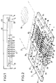
- FIG. 2 seen in perspective, a contact frame 1 of a smart card reader of the known art, with such a smart card 2 in the insertion position.
- This frame essentially comprises a piece of insulating molded material 3 playing both the role of supporting contact elements 4, serving for connection to the chip of card 2, of supporting a limit switch contact 5, indicating that a card is present in the reader and that it is in an adequate position to be read, and, at least, of slide support 6, used for guiding the card and intended to drive it to the appropriate position indicated.
- the contact frame 1 comprises an inner frame 7 constituted by the parts of the frame 1 delimiting the connection windows 8, 9, 10, 11.
- the contact elements 4 extend in these windows, from the bars 12, 13 in which they are molded.
- the contact elements 4 are profiled and protrude above the plane 14 of the surface of the frame 1. They must come into contact with the contact pads of the connection zone 15 of the card 1, when the latter is correctly inserted in the smart card reader.
- This inner frame 7 is extended by two wings 17, 18 which end, opposite the inner frame 7, by slide supports 6, which are simple flat surfaces, provided with at least one centering foot 19, 20.
- FIG. 1 represents an end view of the frame 1 of FIG. 2. It can be seen there that the slides 21 and 22 are formed every two in a piece of molded insulating material 23 forming a cover and which is mounted on the supports 6 of the frame 1. This piece 23 is precisely positioned relative to the frame 1 by the centering feet 19, 20. It guides the card 2 of which it surrounds the edges. As can be seen in FIG. 2, the wings 17, 18 are perforated, to save material, by recesses 24.
- the contact frame 1 also carries the limit switch 5 and a limit stop 25.
- This limit switch 5 is a rest contact, opening when the card, shortly before coming to bear on the end stop 25, actuates the movable blade 26 by pressing on its end 27, which separates it from the fixed contact blade 28.
- the two blades are force-fitted into slots 29, 30 of the frame 1, this which ensures the accuracy of their positioning.
- the stop 25 ensures the correct positioning of the card in the smart card reader.
- the pusher 31 is an elastic blade intended to press the smart card 2 towards the cover 23, which presses it against the face of the slide opposite the contact elements to precisely define its distance from the contact elements 4 .
- the smart card reader comprises a contact frame 40 as shown in FIGS. 1 and 2.
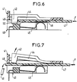
- the cover 41 of said reader is shown in FIGS. 3, 4 and 5.
- It includes a positioning stop retractable 42 which normally fulfills a limit stop function for the card so as to allow electrical connection between the contact elements of the frame and the conductive pads of the smart card, but which disappears when the pressing force exerted by the card exceeds a predetermined value.
- the reader of the invention comprises a guide corridor for the card 43, open, if possible entirely, at its end towards the interior of the device in which said reader is placed. This is so that various foreign objects, introduced by accident or by vandalism, are ejected towards the interior of the device by insertion of the smart card.
- a rib 51, fixed, disposed next to the stop 42 is intended to suitably press the card against the contact elements 45 at said stop and prevents the card, which may possibly have a curvature, from raising the stop. If the stop is even slightly raised, the value of the force F1 to release the opening is reduced.
- the stop and the rib are obtained in the same molding as the cover; the critical tilting force being adjusted by the stiffness of the plastic blade formed by said stop 42; This force can, for example be between 70 and 90 Newtons.
- the stop 42 has an inclined range 50, for example of inclination close to 12 °, against which a card normally inserted in the reader stops, but which causes erasure of the stopper when it is subjected to an abnormally high pressure.
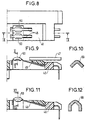
- FIGS. 8 to 12 illustrate several aspects of two advantageous embodiments of the reader of the invention such that it is difficult to damage the contact elements 45 of the frame 40.
- the parts of the contact elements 45 which protrude in the guide corridor of the card, carry cheeks 50.
- these cheeks 50 are small, which facilitates the manufacture of the contact elements by cutting into strips. In this case the passage is almost completely obstructed, the protection against vandalism is therefore effective.
- the cheeks extend into the orifice which has been formed in the contact frame 40 to allow the recoil of the contact element. The passage of an object under contact is thus prevented.
- the invention therefore consists in adding on the parts of the contact elements, which are capable of projecting inside the guide corridor, lateral cheeks 50 in the shape of a Vee or rounded, which closes the access to the face. rear of contacts; these cheeks 50 having a suitable slope so that any object located in the guide corridor and pressing at any point of the contact element pushes the latter out of said corridor, without risk of damage by lateral thrust on the contact element.
Landscapes
- Engineering & Computer Science (AREA)
- Physics & Mathematics (AREA)
- General Physics & Mathematics (AREA)
- Theoretical Computer Science (AREA)
- Artificial Intelligence (AREA)
- Computer Vision & Pattern Recognition (AREA)
- Conveying Record Carriers (AREA)
- Coupling Device And Connection With Printed Circuit (AREA)
- Details Of Connecting Devices For Male And Female Coupling (AREA)
Claims (9)
- Chipkartenlesevorrichtung mit Kontaktelementen (45), Führungs- und Positionierungselementen für eine Karte, insbesondere einem Führungsdurchgang und einem Anschlag (42) zur Positionierung am Ende des Weges, wobei die Anordnung eingerichtet ist, um die elektrische Verbindung zwischen den Kontaktelementen (45) und den leitenden Flächen (46) einer in die Lesevorrichtung bis zum Anschlagen an den Anschlag zur Positionierung am Ende des Weges eingeführten Karte (47)sicherzustellen, dadurch gekennzeichnet, daß
der Anschlag (42) zur Positionierung am Ende des Weges ein zurückziehbarer Anschlag ist, der unter der auf ihn durch die Karte ausgeübten Druckkraft zurückweicht, wenn diese Kraft (F) größer als ein gegebener Wert (F1) ist, und daß der Führungsdurchgang für die Karte an seinem inneren Ende (48) hinter dem zurückziehbaren Anschlag offen ist. - Chipkartenlesevorrichtung nach Anspruch 1, dadurch gekennzeichnet, daß der Anschlag (42) Teil des Deckels (41) der Lesevorrichtung ist.
- Chipkartenlesevorrichtung nach Anspruch 2, dadurch gekennzeichnet, daß der Anschlag (42) am Ende eines beweglichen Arms angeordnet ist, dessen Innenseite eine zentrale Rippe (44) aufweist, die dazu dient, die eingeführte Karte zum Kontaktbereich des Anschlags zu führen.
- Chipkartenlesevorrichtung nach Anspruch 3, dadurch gekennzeichnet, daß der bewegliche Bereich des Anschlags (42) eine geneigte Anlagefläche (50) aufweist, an der eine normal in die Lesevorrichtung eingeführte Karte zum Halten kommt, die aber das Zurückweichen des Anschlags bewirkt, wenn sie einer größeren Druckkraft als dem vorgegebenen Wert (F1) ausgesetzt ist.
- Chipkartenlesevorrichtung nach Anspruch 4, dadurch gekennzeichnet, daß diese Anlagefläche unter in etwa 12° geneigt ist.
- Chipkartenlesevorrichtung nach Anspruch 2, dadurch gekennzeichnet, daß der Deckel (41) eine ortsfeste Rippe (51) aufweist, die neben dem Anschlag (42) angeordnet ist, um die Karte (47) passend gegen die Kontaktelemente in Höhe dieses Anschlags (42) zu drücken.
- Chipkartenlesevorrichtung nach einem der vorhergehenden Ansprüche, dadurch gekennzeichnet, daß die Rippe (51) und der Anschlag (42) bei der Formung des Deckels (41) erhalten werden.
- Chipkartenlesevorrichtung nach einem der vorhergehenden Ansprüche, dadurch gekennzeichnet, daß die Bereiche der Kontaktelemente (45), die in den Führungsdurchgang vorspringen, Seitenwangen (50) tragen.
- Chipkartenlesevorrichtung nach Anspruch 8, dadurch gekennzeichnet, daß die Seitenwangen (50) bis in die Öffnung hinein verlängert sind, die in der Lesevorrichtung gebildet ist, um das Zurückweichen der Kontaktelemente (45) zu ermöglichen.
Applications Claiming Priority (2)
| Application Number | Priority Date | Filing Date | Title |
|---|---|---|---|
| FR9105192A FR2675929B1 (fr) | 1991-04-26 | 1991-04-26 | Lecteur de carte a puce. |
| FR9105192 | 1991-04-26 |
Publications (2)
| Publication Number | Publication Date |
|---|---|
| EP0510599A1 EP0510599A1 (de) | 1992-10-28 |
| EP0510599B1 true EP0510599B1 (de) | 1997-06-04 |
Family
ID=9412306
Family Applications (1)
| Application Number | Title | Priority Date | Filing Date |
|---|---|---|---|
| EP92106862A Expired - Lifetime EP0510599B1 (de) | 1991-04-26 | 1992-04-22 | Chipkartenabtaster |
Country Status (7)
| Country | Link |
|---|---|
| US (1) | US5286957A (de) |
| EP (1) | EP0510599B1 (de) |
| JP (1) | JP2963574B2 (de) |
| AU (1) | AU664363B2 (de) |
| DE (1) | DE69220140T2 (de) |
| ES (1) | ES2103851T3 (de) |
| FR (1) | FR2675929B1 (de) |
Families Citing this family (21)
| Publication number | Priority date | Publication date | Assignee | Title |
|---|---|---|---|---|
| JPH06139414A (ja) * | 1992-10-28 | 1994-05-20 | Sony Corp | Icカード検出装置 |
| DE4408710C5 (de) * | 1994-03-15 | 2008-07-03 | Ddm Hopt + Schuler Gmbh & Co Kg | Kartenleser |
| DE9407499U1 (de) * | 1994-05-05 | 1995-09-07 | Itt Composants Et Instruments, Dole Cedex | Elektrisches Kontaktelement |
| DE69524701T2 (de) * | 1994-09-07 | 2002-08-14 | Hitachi, Ltd. | Staubsicherer tragbarer Chipkartenleser |
| JP2609431B2 (ja) * | 1994-09-22 | 1997-05-14 | 山一電機株式会社 | メモリカード |
| FR2726694B1 (fr) * | 1994-11-07 | 1996-12-06 | Itt Composants Instr | Connecteur electrique pour une carte a memoire electronique comportant des moyens de raccordement electrique du type a deplacement d'isolant |
| DE19502176A1 (de) * | 1995-01-25 | 1996-08-08 | Thomas & Betts Gmbh | Chipkarten-Lesegerät |
| DE19506606C2 (de) * | 1995-02-24 | 1996-12-19 | Amphenol Tuchel Elect | Chipkartenleser |
| JP2690285B2 (ja) * | 1995-06-19 | 1997-12-10 | 山一電機株式会社 | カードの逆挿入防止装置 |
| US5892213A (en) * | 1995-09-21 | 1999-04-06 | Yamaichi Electronics Co., Ltd. | Memory card |
| US5955718A (en) * | 1995-10-06 | 1999-09-21 | Coin Acceptors, Inc. | Integrated credit/information exchange module |
| DE19608990A1 (de) * | 1996-03-08 | 1997-09-11 | Bosch Gmbh Robert | Chipkarte und Kartenleser für Chipkarten |
| AU743049B2 (en) * | 1996-07-11 | 2002-01-17 | Smartmove (Nz) Limited | Smart card acceptor device |
| AU4415697A (en) * | 1996-09-17 | 1998-04-14 | Sherry Brennan | Electronic card valet |
| TW340678U (en) * | 1997-09-10 | 1998-09-11 | Hon Hai Prec Ind Co Ltd | Electronic card adapter |
| JP3288277B2 (ja) * | 1997-09-16 | 2002-06-04 | アルプス電気株式会社 | Icカード用コネクタ |
| USD420647S (en) * | 1998-07-31 | 2000-02-15 | Hon Hai Precision Ind. Co., Ltd. | Smart card connector |
| FR2782849B1 (fr) * | 1998-08-28 | 2000-11-10 | Framatome Connectors Int | Dispositif antivandalisme pour lecteur de carte a puce |
| FR2784766B1 (fr) * | 1998-10-20 | 2001-12-07 | Xiring | Dispositif de lecture de carte a microcircuit |
| EP1231559B1 (de) * | 2001-02-09 | 2003-11-26 | ddm hopt + schuler GmbH & Co. KG | Kartenleser |
| JP5655679B2 (ja) * | 2011-04-05 | 2015-01-21 | 富士通株式会社 | カードアダプタ及び電子装置 |
Family Cites Families (14)
| Publication number | Priority date | Publication date | Assignee | Title |
|---|---|---|---|---|
| US4171737A (en) * | 1977-10-03 | 1979-10-23 | Docutel Corporation | Entry control device |
| US4514623A (en) * | 1983-01-10 | 1985-04-30 | American Magnetics Corporation | Automatic teller machine with entrance adapted to prevent access by foreign objects |
| FR2552252B1 (fr) * | 1983-09-21 | 1987-07-31 | Dassault Electronique | Lecteur mixte pour cartes a piste magnetique et/ou a puce electronique |
| JPS60100829U (ja) * | 1983-12-14 | 1985-07-09 | 第一電子工業株式会社 | メモリカ−ド用コネクタ |
| FR2587132B1 (fr) * | 1985-09-12 | 1987-11-20 | Bull Transac | Procede de confiscation d'une carte pour un lecteur mixte et lecteur mixte |
| JPH0657476B2 (ja) * | 1987-03-27 | 1994-08-03 | 三菱電機株式会社 | Icカ−ドの外部機器用コネクタ |
| EP0458421B1 (de) * | 1987-04-09 | 1999-10-06 | SCHLUMBERGER Systèmes | Einrichtung zum Lesen/Schreiben elektronischer Speicherkarten, gegen Zerstörungswut geschützt |
| US4839509A (en) * | 1987-06-19 | 1989-06-13 | Diesel Kiki Co., Ltd. | Connector device for connecting IC card to reading and/or writing apparatus |
| JPH0775030B2 (ja) * | 1987-08-07 | 1995-08-09 | 沖電気工業株式会社 | カード型集積回路のコネクタ |
| JPH02307182A (ja) * | 1989-05-23 | 1990-12-20 | Hitachi Maxell Ltd | Icカードリーダ・ライタ |
| DE8908801U1 (de) * | 1989-07-19 | 1989-09-07 | Siemens AG, 1000 Berlin und 8000 München | Kartenleser mit einem in einer Aufnahme entgegen Federkraft verschiebbaren Schlitten |
| US5066241A (en) * | 1990-06-18 | 1991-11-19 | Eastman Kodak Company | Electrical connector apparatus for use with an integrated circuit card |
| JPH0486292U (de) * | 1990-11-22 | 1992-07-27 | ||
| US5161992A (en) * | 1992-01-17 | 1992-11-10 | Amp Incorporated | Electrical connector assembly for a card containing an integrated circuit chip |
-
1991
- 1991-04-26 FR FR9105192A patent/FR2675929B1/fr not_active Expired - Fee Related
-
1992
- 1992-04-16 AU AU14958/92A patent/AU664363B2/en not_active Expired - Fee Related
- 1992-04-22 EP EP92106862A patent/EP0510599B1/de not_active Expired - Lifetime
- 1992-04-22 DE DE69220140T patent/DE69220140T2/de not_active Expired - Lifetime
- 1992-04-22 ES ES92106862T patent/ES2103851T3/es not_active Expired - Lifetime
- 1992-04-23 JP JP4104934A patent/JP2963574B2/ja not_active Expired - Lifetime
- 1992-04-23 US US07/872,327 patent/US5286957A/en not_active Expired - Lifetime
Also Published As
| Publication number | Publication date |
|---|---|
| DE69220140D1 (de) | 1997-07-10 |
| EP0510599A1 (de) | 1992-10-28 |
| JP2963574B2 (ja) | 1999-10-18 |
| ES2103851T3 (es) | 1997-10-01 |
| AU1495892A (en) | 1992-10-29 |
| JPH05135215A (ja) | 1993-06-01 |
| FR2675929A1 (fr) | 1992-10-30 |
| AU664363B2 (en) | 1995-11-16 |
| DE69220140T2 (de) | 1998-01-08 |
| US5286957A (en) | 1994-02-15 |
| FR2675929B1 (fr) | 1993-07-02 |
Similar Documents
| Publication | Publication Date | Title |
|---|---|---|
| EP0510599A1 (de) | Chipkartenabtaster | |
| EP1622224B1 (de) | Elektrische Vorrichtung mit automatischer Anschlussklemme | |
| EP0316700A1 (de) | Kontaktrahmen für I.S.-Kartenleser | |
| EP0348929A1 (de) | Chipkartenabtaster | |
| CA2002181A1 (fr) | Recepteur de cartes a puce | |
| FR2791215A1 (fr) | Lecteur de carte sim et telephone mobile le comportant | |
| CH663545A5 (fr) | Ski de fond et chaussure destinee a etre utilisee avec ce ski. | |
| FR2805635A1 (fr) | Lecteur de carte et equipement mobile le comportant | |
| FR2793921A1 (fr) | Ensemble compact pour le raccordement d'une carte a circuit(s) integre(s) comportant des moyens d'ejection de la carte | |
| FR2665029A1 (fr) | Connecteur electrique pour cartes a memoire electronique. | |
| EP0287417B1 (de) | Einrichtung zum Lesen/Schreiben elektronischer Speicherkarten, geschützt gegen Zerstörungswut | |
| FR2755790A1 (fr) | Commutateur a bouton-poussoir miniature, notamment pour une unite de disque souple | |
| EP0785606B1 (de) | Vorrichtung zum Befestigen eines elektrischen Gerätes | |
| EP0981796B1 (de) | Elektrischer verbinder für eine kontaktkarte mit integrierten schaltungen | |
| EP0178974B1 (de) | Verbindungseinrichtungen für gedruckte Schaltungen | |
| EP2456021A1 (de) | Stromsteckdose mit seitlichen verschiebbaren Balken | |
| CH663544A5 (fr) | Ski de fond et chaussure destinee a etre utilisee avec ce ski. | |
| FR2844642A1 (fr) | Connecteur electrique pour une carte a memoire electronique a grande capacite de stockage | |
| EP0656597B1 (de) | Kartenkontaktrahmen und -verbinder | |
| FR2862784A1 (fr) | Dispositif pour le raccordement electrique d'une carte a puce | |
| FR2713406A1 (fr) | Cadre de contact et connecteur pour carte. | |
| FR2712430A1 (fr) | Connecteur électrique et lecteur de carte le comportant. | |
| EP0147293B1 (de) | Elektrische Schaltvorrichtung | |
| FR2537349A1 (fr) | Dispositif de connexion a contacts et procede de montage desdits contacts dans le dispositif | |
| FR2778996A1 (fr) | Terminal de paiement portable capable de traiter des cartes a puce et des cartes magnetiques |
Legal Events
| Date | Code | Title | Description |
|---|---|---|---|
| PUAI | Public reference made under article 153(3) epc to a published international application that has entered the european phase |
Free format text: ORIGINAL CODE: 0009012 |
|
| AK | Designated contracting states |
Kind code of ref document: A1 Designated state(s): BE CH DE ES FR GB IT LI NL |
|
| 17P | Request for examination filed |
Effective date: 19921207 |
|
| 17Q | First examination report despatched |
Effective date: 19950810 |
|
| RAP1 | Party data changed (applicant data changed or rights of an application transferred) |
Owner name: FRAMATOME CONNECTORS PONTARLIER |
|
| GRAG | Despatch of communication of intention to grant |
Free format text: ORIGINAL CODE: EPIDOS AGRA |
|
| GRAH | Despatch of communication of intention to grant a patent |
Free format text: ORIGINAL CODE: EPIDOS IGRA |
|
| GRAH | Despatch of communication of intention to grant a patent |
Free format text: ORIGINAL CODE: EPIDOS IGRA |
|
| GRAA | (expected) grant |
Free format text: ORIGINAL CODE: 0009210 |
|
| AK | Designated contracting states |
Kind code of ref document: B1 Designated state(s): BE CH DE ES FR GB IT LI NL |
|
| REG | Reference to a national code |
Ref country code: CH Ref legal event code: EP |
|
| GBT | Gb: translation of ep patent filed (gb section 77(6)(a)/1977) |
Effective date: 19970613 |
|
| REF | Corresponds to: |
Ref document number: 69220140 Country of ref document: DE Date of ref document: 19970710 |
|
| REG | Reference to a national code |
Ref country code: CH Ref legal event code: NV Representative=s name: SCHMAUDER & WANN PATENTANWALTSBUERO, INHABER KLAUS |
|
| ITF | It: translation for a ep patent filed | ||
| REG | Reference to a national code |
Ref country code: ES Ref legal event code: FG2A Ref document number: 2103851 Country of ref document: ES Kind code of ref document: T3 |
|
| PLBE | No opposition filed within time limit |
Free format text: ORIGINAL CODE: 0009261 |
|
| STAA | Information on the status of an ep patent application or granted ep patent |
Free format text: STATUS: NO OPPOSITION FILED WITHIN TIME LIMIT |
|
| 26N | No opposition filed | ||
| REG | Reference to a national code |
Ref country code: GB Ref legal event code: IF02 |
|
| PGFP | Annual fee paid to national office [announced via postgrant information from national office to epo] |
Ref country code: GB Payment date: 20070313 Year of fee payment: 16 |
|
| PGFP | Annual fee paid to national office [announced via postgrant information from national office to epo] |
Ref country code: NL Payment date: 20070315 Year of fee payment: 16 |
|
| PGFP | Annual fee paid to national office [announced via postgrant information from national office to epo] |
Ref country code: ES Payment date: 20070417 Year of fee payment: 16 |
|
| PGFP | Annual fee paid to national office [announced via postgrant information from national office to epo] |
Ref country code: CH Payment date: 20070427 Year of fee payment: 16 |
|
| PGFP | Annual fee paid to national office [announced via postgrant information from national office to epo] |
Ref country code: IT Payment date: 20070616 Year of fee payment: 16 Ref country code: BE Payment date: 20070430 Year of fee payment: 16 |
|
| BERE | Be: lapsed |
Owner name: *FRAMATOME CONNECTORS PONTARLIER Effective date: 20080430 |
|
| REG | Reference to a national code |
Ref country code: CH Ref legal event code: PL |
|
| GBPC | Gb: european patent ceased through non-payment of renewal fee |
Effective date: 20080422 |
|
| NLV4 | Nl: lapsed or anulled due to non-payment of the annual fee |
Effective date: 20081101 |
|
| PG25 | Lapsed in a contracting state [announced via postgrant information from national office to epo] |
Ref country code: NL Free format text: LAPSE BECAUSE OF NON-PAYMENT OF DUE FEES Effective date: 20081101 Ref country code: LI Free format text: LAPSE BECAUSE OF NON-PAYMENT OF DUE FEES Effective date: 20080430 Ref country code: CH Free format text: LAPSE BECAUSE OF NON-PAYMENT OF DUE FEES Effective date: 20080430 |
|
| PG25 | Lapsed in a contracting state [announced via postgrant information from national office to epo] |
Ref country code: BE Free format text: LAPSE BECAUSE OF NON-PAYMENT OF DUE FEES Effective date: 20080430 |
|
| REG | Reference to a national code |
Ref country code: ES Ref legal event code: FD2A Effective date: 20080423 |
|
| PG25 | Lapsed in a contracting state [announced via postgrant information from national office to epo] |
Ref country code: GB Free format text: LAPSE BECAUSE OF NON-PAYMENT OF DUE FEES Effective date: 20080422 |
|
| PG25 | Lapsed in a contracting state [announced via postgrant information from national office to epo] |
Ref country code: ES Free format text: LAPSE BECAUSE OF NON-PAYMENT OF DUE FEES Effective date: 20080423 |
|
| PG25 | Lapsed in a contracting state [announced via postgrant information from national office to epo] |
Ref country code: IT Free format text: LAPSE BECAUSE OF NON-PAYMENT OF DUE FEES Effective date: 20080422 |
|
| PGFP | Annual fee paid to national office [announced via postgrant information from national office to epo] |
Ref country code: FR Payment date: 20110331 Year of fee payment: 20 |
|
| PGFP | Annual fee paid to national office [announced via postgrant information from national office to epo] |
Ref country code: DE Payment date: 20110429 Year of fee payment: 20 |
|
| REG | Reference to a national code |
Ref country code: DE Ref legal event code: R071 Ref document number: 69220140 Country of ref document: DE |
|
| REG | Reference to a national code |
Ref country code: DE Ref legal event code: R071 Ref document number: 69220140 Country of ref document: DE |
|
| PG25 | Lapsed in a contracting state [announced via postgrant information from national office to epo] |
Ref country code: DE Free format text: LAPSE BECAUSE OF EXPIRATION OF PROTECTION Effective date: 20120423 |