EP0511059B1 - Verfahren und Vorrichtung zur Regelung des transversalen Magnetfelds in einem Undulator zur Erzeugung von Lichtenergie aus einem Elektronenstrahl - Google Patents
Verfahren und Vorrichtung zur Regelung des transversalen Magnetfelds in einem Undulator zur Erzeugung von Lichtenergie aus einem Elektronenstrahl Download PDFInfo
- Publication number
- EP0511059B1 EP0511059B1 EP92401082A EP92401082A EP0511059B1 EP 0511059 B1 EP0511059 B1 EP 0511059B1 EP 92401082 A EP92401082 A EP 92401082A EP 92401082 A EP92401082 A EP 92401082A EP 0511059 B1 EP0511059 B1 EP 0511059B1
- Authority
- EP
- European Patent Office
- Prior art keywords
- conductor
- undulator
- magnetic field
- electron beam
- transverse magnetic
- Prior art date
- Legal status (The legal status is an assumption and is not a legal conclusion. Google has not performed a legal analysis and makes no representation as to the accuracy of the status listed.)
- Expired - Lifetime
Links
- 238000010894 electron beam technology Methods 0.000 title claims description 39
- 238000000034 method Methods 0.000 title claims description 8
- 239000004020 conductor Substances 0.000 claims description 76
- 230000005284 excitation Effects 0.000 claims description 30
- 238000004804 winding Methods 0.000 claims description 23
- 230000001939 inductive effect Effects 0.000 claims description 14
- 230000005415 magnetization Effects 0.000 claims description 13
- 238000011144 upstream manufacturing Methods 0.000 claims description 6
- 238000010079 rubber tapping Methods 0.000 claims 8
- 230000003287 optical effect Effects 0.000 description 16
- 239000003574 free electron Substances 0.000 description 6
- 230000003993 interaction Effects 0.000 description 4
- 238000010586 diagram Methods 0.000 description 3
- 230000006698 induction Effects 0.000 description 3
- 230000005684 electric field Effects 0.000 description 2
- 238000000605 extraction Methods 0.000 description 2
- 125000006850 spacer group Chemical group 0.000 description 2
- 230000001133 acceleration Effects 0.000 description 1
- 238000006243 chemical reaction Methods 0.000 description 1
- 238000001816 cooling Methods 0.000 description 1
- 239000002184 metal Substances 0.000 description 1
- 230000010355 oscillation Effects 0.000 description 1
- 230000005855 radiation Effects 0.000 description 1
- 238000004904 shortening Methods 0.000 description 1
- 230000001360 synchronised effect Effects 0.000 description 1
Images



Classifications
-
- H—ELECTRICITY
- H01—ELECTRIC ELEMENTS
- H01S—DEVICES USING THE PROCESS OF LIGHT AMPLIFICATION BY STIMULATED EMISSION OF RADIATION [LASER] TO AMPLIFY OR GENERATE LIGHT; DEVICES USING STIMULATED EMISSION OF ELECTROMAGNETIC RADIATION IN WAVE RANGES OTHER THAN OPTICAL
- H01S3/00—Lasers, i.e. devices using stimulated emission of electromagnetic radiation in the infrared, visible or ultraviolet wave range
- H01S3/09—Processes or apparatus for excitation, e.g. pumping
- H01S3/0903—Free-electron laser
Definitions
- the invention relates to devices called inverters, which allow, in Free Electron Lasers (LEL), the direct conversion of part of the energy of a relativistic electron beam into light energy.
- LEL Free Electron Lasers
- the operating principle of the Free Electron Laser is based on the braking radiation which results from the fact that any electron undergoing acceleration or deceleration radiates electromagnetic energy and on the relativistic shortening of the wavelength.
- the electrons passing through an alternately polarized transverse magnetic field undergo, as shown in FIG. 2, deflections of small amplitudes, sometimes in one direction, sometimes in the other, and radiate light energy in the beam propagation direction.
- deflections of small amplitudes sometimes in one direction, sometimes in the other, and radiate light energy in the beam propagation direction.
- the wavelength of the light emission is shorter the smaller the magnetic pitch of the inverter ⁇ ond.
- the present invention relates, more particularly, to inverters whose transverse magnetic field is generated, in whole or in part, by an excitation current flowing in a conductor forming windings or meanders along the path of the electron beam in the optical cavity of a free electron laser.
- Its purpose is to improve the interaction of electrons and light energy radiated within the inverter.
- the partial auxiliary currents injected by the auxiliary taps have intensities which are constant over a period of one to two microseconds and then decrease until they cancel out in one or two microseconds.
- the invention also relates to an inverter for implementing the above method.
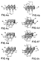
- This electrical conductor which then constitutes the magnetization circuit of the inverter can take various forms. It can be in a single part as shown in 31, 35, 39, 43 in Figures 4a, 4c, 4th, and 4g.
- meanders which can be either triangular in outline as shown in 31, 33, 34 in Figures 4a and 4b, or in rectangular U-shaped outline as shown in 35, 37, 38 in Figures 4e and 4d or in ⁇ as shown in 39, 41, 42 in Figures 4e and 4f, or with a rounded outline as shown in 43, 45, 46 in Figures 4g and 4h.
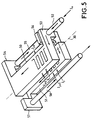
- FIG. 5 An example is given in Figure 5 where there are two parts 50, 51 shown schematically, of a meandering conductor of the magnetization circuit.
- the excitation current arrives via a conductive bar 52 fixed to a conductive lateral tab 53 forming a first end of the part 50 of the meander conductor arranged in the axis and above the path 30 of the beam. electrons.
- the excitation current flows through this part 50 and leaves it via its second end which forms a conductive lateral tab 54 arranged on the same side.
- This lateral tab 54 is fixed to a conductive bar 55 of interconnection between the two parts 50 and 51 of the meander conductor which returns towards the first end of the part 50 and meets, before the lateral tab 53 of the latter, a another side tab 56 forming a first end of the part 51 of the meander conductor disposed in the axis below the path 30 of the electron beam.
- the excitation current returns via the interconnection busbar 55 towards the first end of the part 51 of the meander conductor and then flows through this part 51 in the same direction as the part 50 and leaves therefrom by a second end which forms a conductive lateral tab 57 protruding from the side opposite to the other lateral tabs 53, 54, 56 and which is connected to a conductive bar 58 for starting the current along the two parts 50 and 51 of the meandering conductor.
- the electrons coming from a radiofrequency linear accelerator propagate in bursts which correspond to micro pulses of a few tens of picoseconds and which are grouped by a few thousand in isolated packets corresponding to macro pulses of a few tens of microseconds to a few seconds.
- the operation of the electron-light energy interaction radiated within the inverter placed in the optical cavity of the Laser can be improved by varying the value of the transverse magnetic field of the inverter during a macro pulse at the times as a function of time and of the position along the path of the electron beam in the optical cavity so that, during the increase in power of the electron-radiated energy interaction following the arrival of a packet of puffs of electrons in the inverter, the law of variation of the synchronous speed along the inverter is, at each instant, the optimal law corresponding to the instantaneous level of the high frequency electric field.
- auxiliary jacks I j , I j + 1 are added via the auxiliary bypass sockets, over a period of time less than one or two microseconds at the start of each macro pulse, which are added to the main current I o in the parts of the conductor inducing the transverse magnetic field located relative to these sockets, upstream with respect to the direction of movement of the beam electrons. Then these auxiliary currents are made to decrease until their cancellation over a subsequent duration also less than one or two microseconds while maintaining constant the intensity of the main excitation current over the entire duration of a macro-pulse.
- the initial intensities of the auxiliary currents I j and I j + 1 as well as their laws of decay during each macro pulse are adjusted experimentally so as to optimize the yield of light energy.
- FIG. 7 gives an example of an electrical current supply circuit of an inverter having a magnetization circuit consisting of a meandering conductor 60 in a single part such as those represented in FIGS. 4a, 4c, 4e or 4g.
- the electron beam circulates along the meandering conductor 60 inside a series of holes drilled longitudinally from the end S to the end E in the direction of the arrow 61.
- the meandering conductor 60 is provided with auxiliary current bypass sockets P1 ..., P j ..., P n staggered along its length and supplied with current via a pulse transformer 62.
- the pulse transformer 62 comprises a primary winding 63 and a secondary winding 64 with an intermediate tap 65.
- the meander conductor 60 is connected by its end S to an end terminal 66 of the secondary winding 64 and by its end E to the intermediate tap 65.
- the other end terminal 67 of the secondary winding 64 of the pulse transformer 62 is connected via the collector-emitter junctions of current switching transistors T1 ..., T j ..., T n aux taken auxi branch links P1 ..., P j ..., P n of the meandering conductor 60.
- the bases of the current switching transistors T1 ..., T j ..., T n are connected to a control circuit 68 .
- the pulse transformer 62 receives on its primary winding 63 excitation pulses which each cover, with a slightly longer duration, a macro pulse coinciding with the arrival in the inverter of a packet of puffs d 'electrons.
- Each excitation pulse causes the appearance, on the intermediate tap 65 of the secondary winding 64 of the pulse transformer 62, of a main current I o , of an intensity of a few kiloamperes to a few tens of kiloamperes which circulates on the entire length of the meandering conductor.
- the current switching transistors T1 ..., T j ..., T n are progressively blocked by the control circuit 68 over a duration t2 - t1 less than one or two microseconds in order to eliminate the partial auxiliary currents and to obtain a current variation law similar in shape to that shown in FIG. 6.
- FIG. 8 gives an example of an electrical current supply circuit of an inverter having a magnetization circuit consisting of a meander conductor in two parts 70, 71 such as those shown in FIGS. 4b, 4d, 4f or 4h.
- the electron beam circulates along the meander conductor between its two parts 70, 71, from their end S to their end E. in the direction of the arrow 72.
- the two parts 70, 71 of the meander conductor are provided with auxiliary current taps P′1 ..., P ′ j ..., P ′ n and respectively P respectivement ..., P ⁇ j ..., P ⁇ n staggered along their length.
- the part 70 of the meander conductor is connected by its end E to the intermediate socket 76 and by its end S to a resistor 77 leading to the end E of the other part 71 whose end S is connected to a terminal of end 78 of the secondary winding 75 of the pulse transformer 73.
- the other end terminal 79 of the secondary winding 75 of the pulse transformer 73 is connected via the collector-emitter junctions of a group of current-switching transistors T′1 ..., T ′ j ..., T ′ n to the auxiliary branch taps P′1 ..., P ′ j ..., P ′ n of part 70 of the conductor meandered while the auxiliary taps P ⁇ 1 ..., P ⁇ j ..., P ⁇ n of the other part 71 of the meandered conductor are connected via the collector-emitter junctions of a other group of current switching transistors T ⁇ 1 ..., T ⁇ j ..., T ⁇ n at the end S of the p first part 70 of the meandering conductor.
- the bases of the current switching transistors T′1 ..., T ′ j ..., T ′ n and T ⁇ 1 ..., T ⁇ j ..., T ⁇ n of the two groups are connected to a
- the pulse transformer 73 receives on its primary winding 74 excitation pulses which each cover, with a slightly longer duration, a macro pulse coinciding with the arrival in the inverter of a packet of puffs d 'electrons.
- Each excitation pulse causes the appearance, on the intermediate tap 76 of the secondary winding 75 of the pulse transformer 73, of a main current I o with an intensity of a few kiloamperes to a few tens of kiloamperes which circulates over the entire length of two parts 70, 71 of the meander conductor, in the same direction in each of the two parts with respect to the path of the electron beam.
- P ′ n and which are on the other hand taken at the outlet of part 70 of the meander conductor to be injected into other part 71 of the meandered conductor at the various auxiliary bypass sockets P ⁇ 1, .. P ⁇ j , .. P ⁇ n .
- the resistor 77 placed at the head of the part 71 of the meander conductor compensates for the resistances in the on state of the transistors T ⁇ 1, .. T ⁇ j , .. T ⁇ n to allow the extraction of the partial currents I1, I j , I n at the outlet of part 70 of the meandering conductor.
- the two parts 70, 71 of the meandering conductor are traversed by identical currents which increase when one moves from their end E to their end S in a direction opposite to the direction 72 of path of the electron beam.
- the two groups of current switching transistors T′1, .. T ′ j , .. T ′ n and T ⁇ 1, .. T ⁇ j , .. T ⁇ n are gradually blocked on a duration t2 - t1 of less than one or two microseconds in order to eliminate the partial currents and to obtain a law of variation of current of shape similar to that represented in FIG. 6.
- FIG. 9 gives another example of an electrical current supply circuit for an inverter having a magnetization circuit consisting of a two-part meander conductor 85, 86.
- the electron beam circulates along the conductor at meanders, between its two parts 85, 86 from their end S to their end E in the direction of the arrow 87.
- the two parts 85, 86 of the meander conductor are provided, as before, with auxiliary taps for bypassing current P′1, .. P ′ j , .. P ′ n and respectively P ⁇ 1, .. P ⁇ j , .. P ⁇ n staggered along their length.
- a pulse transformer 88 comprising a primary winding 89 and a secondary winding 90 with intermediate plug 91.
- the part 85 of the meander conductor has its end E connected to the intermediate plug 91 and its end S connected to the end E of the other part 86 of which l the other end S is connected via a resistor 92 to an end terminal 93 of the secondary winding 90 of the pulse transformer 88.
- the other end terminal 94 of the secondary winding 90 of the pulse transformer 88 is connected via the collector-emitter junctions of two groups of current switching transistors T′1, .. T ′ j , .. T ′ n and T ⁇ 1, ..
- a current switching transistor T ′′′ has its collector-emitter junction connected in series with a resistor 95 between the end S of the part 85 of the meander conductor and the end terminal 93 of the secondary winding 90 of the transformer pulses 88.
- the bases of the current switching transistors T′1, .. T ′ j , .. T ′ n and T ⁇ 1, .. T ⁇ j , .. T ⁇ n of the two groups as well as that of the transistors T ′′′ Are connected to a control circuit 96.
- the pulse transformer 88 receives on its primary winding 89 excitation pulses which each cover, with a slightly longer duration, a macro pulse coinciding with the arrival in the inverter of a packet of bursts of electrons.
- Each excitation pulse causes the appearance, on the intermediate tap 91 of the secondary winding 90 of the current transformer 88, of a main current I o of an intensity of a few kiloamperes to a few tens of kiloamperes which flows over the whole the length of the two parts 85, 86 of the meander conductor, in the same direction in each of the two parts relative to the path of the electron beam.
- the resistor 95 makes it possible to adjust the intensity of the current extracted between the two parts 85, 86 of the meander conductor by the transistor T ′′′, so that the latter corresponds well to those of the partial currents.
- the two parts 85, 86 of the meander conductor are traversed by identical currents whose intensity increases when one moves from their end E to their end S in a direction opposite to the direction 87 path of the electron beam.
- the two groups of current switching transistors T′1, .. T ′ j , .. T ′ n ; T ⁇ 1, .. T ⁇ j , .. T ⁇ n and the transistor T ′′′ are progressively blocked over a period t2 - t1 less than one or two microseconds in order to remove the partial auxiliary currents and to obtain in the two parts 85, 86 of the driver meandering a current variation law similar in shape to that shown in Figure 6.
- FIGS. 10 and 11 illustrate an embodiment of an inverter structure having a magnetization circuit formed by a meandering conductor in two superimposed parts 50, 51 electrically assembled in series as in FIG. 5 and provided with auxiliary bypass sockets of current staggered along their length.
- the two superimposed parts 50, 51 of the meander conductor are separated by insulating spacers 100, 101 so as to leave between them a free space 102 for the circulation of the electron beam. They are held in place by two sets of longitudinal bars, not shown, bolted together which pinch them by side in abutment on the insulating spacers 100, 101.
- the assembly of the two parts 50, 51 of the meander conductor, of their holding and interconnection bars 52, 55, 58 as well as cooling pipes not shown so as not to overload the figures is placed in a vacuum box having a U-shaped section wall 103 closed at its base by a base 104 and at its ends by lids.
- the two parts 50 and 51 of the meander conductor which form meanders with a rectangular U-shaped contour as shown in FIG. 4d, have, along one of their side down of the vacuum box, electrical bypass sockets staggered every three meanders.
- These bypass sockets each consist of a piece of metal rod 105, 106 planted laterally in the parts 50, 51 of the meander conductor and connected by a connection wire 107, 108 to an insulating and watertight electrical bushing 109, 110, fixed in the vicinity, through the wall 103 of the vacuum box.
- the electrical bypass sockets on the parts 50, 51 of the meander conductor are placed symmetrically with respect to the intermediate plane which is located between the two parts 50, 51 of the meander conductor and in which the electron beam circulates according to the direction of the arrow 111.
Landscapes
- Physics & Mathematics (AREA)
- Electromagnetism (AREA)
- Engineering & Computer Science (AREA)
- Plasma & Fusion (AREA)
- Optics & Photonics (AREA)
- Lasers (AREA)
- Particle Accelerators (AREA)
Claims (7)
- Verfahren zur Einstellung des transversalen Magnetfelds in einem Undulator für die Erzeugung von Lichtenergie ausgehend von einem Strahl von in isolierten Paketen ausgesendeten Elektronen, wobei ein Paket die Dauer eines Makroimpulses besitzt und der Undulator einen Leiter (60) aufweist, der entlang der Bahn des Elektronenstrahls Windungen oder Mäander bildet, die insgesamt oder in einem Teil ein transversales Magnetfeld induzieren, das abwechselnd Nord-Süd und Süd-Nord polarisiert ist, dadurch gekennzeichnet, daß das Verfahren darin besteht,- auf dem das transversale Magnetfeld induzierenden Leiter Hilfsanschlüsse zur Stromableitung (P₁, ..., Pj, ..., Pn) vorzusehen, die entlang der Bahn des Elektronenstrahls im Undulator verteilt sind,- einen Hauptanregungsstrom (Io) in den ganzen Leiter einzuspeisen, der das transversale Magnetfeld während der Dauer eines Makroimpulses entsprechend der Durchlaufzeit eines Elektronenpakets im Undulator induziert,- und über die Hilfsableitanschlüsse (P₁,..., Pj, ..., Pn) zu Beginn jedes Makroimpulses partielle Ströme (Ij,) einzuspeisen, die sich dem Hauptanregungsstrom (Io) in Teilen des Leiters überlagern und ein transversales Magnetfeld in Zonen der Elektronenstrahlbahn im Undulator induzieren, die sich vor den Ableitungsanschlüssen (P1, ..., Pj, ..., Pn) bezüglich der Bewegungsrichtung der Elektronen des Strahls befinden.
- Verfahren nach Anspruch 1, dadurch gekennzeichnet, daß die partiellen Ströme (Ij), die über die Hilfsableitanschlüsse (P₁, ..., Pj, ..., Pn) eingespeist werden, während einer ersten Zeitperiode eines Makroimpulses konstant gehalten werden und dann während einer zweiten Zeitperiode eines Makroimpulses zunehmend bis auf Null verringert werden.
- Verfahren nach Anspruch 2, dadurch gekennzeichnet, daß die erste Zeitperiode einige Mikrosekunden andauert.
- Verfahren nach Anspruch 2, dadurch gekennzeichnet, daß die zweite Zeitperiode einige Mikrosekunden andauert.
- Undulator für die Erzeugung von Lichtenergie ausgehend von einem Strahl von Elektronen, die in isolierten und mit Makroimpulsen zusammenfallenden Paketen ausgesendet werden, mit einem Magnetkreis, der einen entlang der Bahn des Elektronenstrahls Windungen oder Mäander bildenden Leiter aufweist und ein transversales Magnetfeld induziert, welches abwechselnd Nord-Süd und Süd-Nord polarisiert ist, dadurch gekennzeichnet, daß er weiter aufweist:- Hilfsanschlüsse zur Stromableitung (P₁,..., Pj, ..., Pn), die über den Leiter verteilt sind, der das transversale Magnetfeld entlang der Elektronenstrahlbahn im Undulator induziert,- Mittel, um einen Hauptanregungsstrom (Io) in den ganzen Leiter einzuspeisen, der das transversale Magnetfeld während der Dauer jedes Makroimpulses entsprechend der Durchlaufzeit eines Pakets von Elektronen durch den Undulator induziert, und- Mittel, um über die Hilfsableitanschlüsse (P₁, ..., Pj, ..., Pn) zu Beginn jedes Makroimpulses Hilfsströme (IJ) einzuspeisen, die sich dem Hauptanregungsstrom (Io) in Teilen des Leiters überlagern und ein transversales Magnetfeld in Zonen der Elektronenstrahlbahn im Undulator induzieren, die sich bezüglich der Richtung der Bewegung der Elektronen vor den Ableitanschlüssen befinden.
- Undulator nach Anspruch 5, dadurch gekennzeichnet, daß die Mittel zum Einspeisen der Hilfsströme (Ij) Schaltmittel (T, T′, T˝, T‴) aufweisen, die die Hilfsströme (Ij) eine gewisse Zeit nach dem Beginn jedes Makroimpulses zunehmend sperren.
- Undulator nach Anspruch 5, mit einem Magnetisierungskreis, der einen mäanderförmigen Leiter aus zwei Teilen (50, 51) besitzt, die zu beiden Seiten der Elektronenstrahlbahn liegen, dadurch gekennzeichnet, daß er Hilfsanschlüsse zur Stromableitung (105, 106) aufweist, die entlang der beiden Teile (50, 51) des mäanderförmigen Leiters verteilt sind und symmetrisch bezüglich einer Zwischenebene angeordnet sind, die zwischen den beiden Teilen (50, 51) des mäanderförmigen Leiters liegt und in der der Elektronenstrahl verläuft.
Applications Claiming Priority (2)
| Application Number | Priority Date | Filing Date | Title |
|---|---|---|---|
| FR9105109 | 1991-04-25 | ||
| FR9105109A FR2675959B1 (fr) | 1991-04-25 | 1991-04-25 | Procede et dispositif de reglage du champ magnetique transverse dans un onduleur pour la generation d'energie lumineuse a partir d'un faisceau d'electrons. |
Publications (2)
| Publication Number | Publication Date |
|---|---|
| EP0511059A1 EP0511059A1 (de) | 1992-10-28 |
| EP0511059B1 true EP0511059B1 (de) | 1994-11-09 |
Family
ID=9412247
Family Applications (1)
| Application Number | Title | Priority Date | Filing Date |
|---|---|---|---|
| EP92401082A Expired - Lifetime EP0511059B1 (de) | 1991-04-25 | 1992-04-17 | Verfahren und Vorrichtung zur Regelung des transversalen Magnetfelds in einem Undulator zur Erzeugung von Lichtenergie aus einem Elektronenstrahl |
Country Status (5)
| Country | Link |
|---|---|
| US (1) | US5263035A (de) |
| EP (1) | EP0511059B1 (de) |
| JP (1) | JPH06163198A (de) |
| DE (1) | DE69200643T2 (de) |
| FR (1) | FR2675959B1 (de) |
Families Citing this family (9)
| Publication number | Priority date | Publication date | Assignee | Title |
|---|---|---|---|---|
| JPH0810279B2 (ja) * | 1992-04-28 | 1996-01-31 | 日本原子力研究所 | 円偏光及び垂直直線偏光特性を持つ放射光を得るための挿入光源用磁場発生装置 |
| JPH05326196A (ja) * | 1992-05-22 | 1993-12-10 | Mitsubishi Electric Corp | アンジュレータ |
| US6137811A (en) * | 1993-07-29 | 2000-10-24 | The United States Of America As Represented By The Secretary Of The Navy | System for conditioning an electron beam for improved free-electron laser operation |
| US5475703A (en) * | 1994-04-29 | 1995-12-12 | Scalise; Stanley J. | Radio frequency-excited gas laser |
| US5790573A (en) * | 1996-07-16 | 1998-08-04 | Heller; Robert | High power free electron lasing device using electrostatic wigglers with recirculating beams between a pair of magnetic mirrors |
| RU2267842C2 (ru) * | 2003-12-15 | 2006-01-10 | Российская Федерация, от имени которой выступает государственный заказчик - Министерство Российской Федерации по атомной энергии-Минатом РФ | Способ и устройство для получения электромагнитного излучения оптического диапазона |
| RU2285986C1 (ru) * | 2005-03-05 | 2006-10-20 | Российская Федерация, от имени которой выступает Государственный заказчик - Федеральное агентство по атомной энергии | Устройство для получения электромагнитного излучения оптического диапазона |
| WO2013110320A1 (en) * | 2012-01-24 | 2013-08-01 | Telefonaktiebolaget L M Ericsson (Publ) | Apparatus and method for optimizing the reconfiguration of an optical network |
| US10249420B2 (en) * | 2015-12-08 | 2019-04-02 | Uchicago Argonne, Llc | Continuous winding magnets using thin film conductors without resistive joints |
Family Cites Families (3)
| Publication number | Priority date | Publication date | Assignee | Title |
|---|---|---|---|---|
| US3822410A (en) * | 1972-05-08 | 1974-07-02 | J Madey | Stimulated emission of radiation in periodically deflected electron beam |
| US4542510A (en) * | 1983-08-26 | 1985-09-17 | Rockwell International Corporation | Low inductance magnetic wiggler |
| FR2650447A1 (fr) * | 1989-07-25 | 1991-02-01 | Commissariat Energie Atomique | Laser a electrons libres, a onduleur en milieu gazeux |
-
1991
- 1991-04-25 FR FR9105109A patent/FR2675959B1/fr not_active Expired - Fee Related
-
1992
- 1992-04-17 EP EP92401082A patent/EP0511059B1/de not_active Expired - Lifetime
- 1992-04-17 DE DE69200643T patent/DE69200643T2/de not_active Expired - Lifetime
- 1992-04-17 US US07/869,962 patent/US5263035A/en not_active Expired - Fee Related
- 1992-04-27 JP JP4134182A patent/JPH06163198A/ja active Pending
Also Published As
| Publication number | Publication date |
|---|---|
| DE69200643D1 (de) | 1994-12-15 |
| EP0511059A1 (de) | 1992-10-28 |
| US5263035A (en) | 1993-11-16 |
| FR2675959B1 (fr) | 1993-07-09 |
| JPH06163198A (ja) | 1994-06-10 |
| FR2675959A1 (fr) | 1992-10-30 |
| DE69200643T2 (de) | 1995-03-09 |
Similar Documents
| Publication | Publication Date | Title |
|---|---|---|
| EP0511059B1 (de) | Verfahren und Vorrichtung zur Regelung des transversalen Magnetfelds in einem Undulator zur Erzeugung von Lichtenergie aus einem Elektronenstrahl | |
| EP0360655B1 (de) | Vorrichtung zur beidseitigen Bestrahlung eines Produktes | |
| FR2691602A1 (fr) | Accélérateur linéaire de protons à focalisation améliorée et impédance shunt élevée. | |
| JP3510016B2 (ja) | 磁気発生装置 | |
| EP0496681A1 (de) | Vorrichtung zur Verteilung von Mikrowellenenergie zur Plasmaanregung | |
| EP0737989A1 (de) | Schaltnetzteil mit einem sättigbaren Induktor zur Gestaltung einer Pulsstromquelle | |
| EP1130949B1 (de) | Elektromagnetische Vorrichtung zur Erzeugung von kalten Atomen | |
| JP2890068B2 (ja) | 自由電子レーザ | |
| Miki et al. | Guiding of electrical discharges under atmospheric air by ultraviolet laser‐produced plasma channel | |
| FR2458888A1 (fr) | Dispositif a decharge electronique a champs croises | |
| US4542510A (en) | Low inductance magnetic wiggler | |
| US4388720A (en) | External control of recombination rate for electron-ion recombination lasers | |
| FR2472830A1 (fr) | Dispositif de commande de conduction electrique en mode a champs croises en plasma | |
| Kurtz et al. | Two photon fluorescence displays with a non-mode-locked Nd: YAG laser | |
| WO1986003881A1 (fr) | Aimant solenoidal sans fer | |
| EP0514255B1 (de) | Elektronzyklotronresonanz-Ionenquelle | |
| EP0221920B1 (de) | Elektromagnet mit hoher homogenität des magnetfeldes | |
| FR2632804A1 (fr) | Accelerateur electrostatique de particules, a fonctionnement en regime impulsionnel | |
| EP0814563A1 (de) | Impulsversorgungseinrichtung mit einem Netz von Spulen | |
| FR2674781A1 (fr) | Dispositif inductif compact d'apport de chaleur pour realiser de petites soudures sur des pieces metalliques. | |
| BE652665A (fr) | Dispositif de chauffage par induction | |
| BE460584A (de) | ||
| FR2687254A1 (fr) | Onduleur pour la generation d'energie lumineuse a partir d'un faisceau d'electrons. | |
| EP0598670A1 (de) | Schalt-Anordnung und Steuerungs-Verfahren zur Ausführung einer solchen Anordnung | |
| CH369199A (fr) | Transformateur stabilisateur de tension |
Legal Events
| Date | Code | Title | Description |
|---|---|---|---|
| PUAI | Public reference made under article 153(3) epc to a published international application that has entered the european phase |
Free format text: ORIGINAL CODE: 0009012 |
|
| AK | Designated contracting states |
Kind code of ref document: A1 Designated state(s): DE FR GB IT NL |
|
| 17P | Request for examination filed |
Effective date: 19921109 |
|
| RAP1 | Party data changed (applicant data changed or rights of an application transferred) |
Owner name: THOMSON-CSF |
|
| 17Q | First examination report despatched |
Effective date: 19940301 |
|
| GRAA | (expected) grant |
Free format text: ORIGINAL CODE: 0009210 |
|
| RIN1 | Information on inventor provided before grant (corrected) |
Inventor name: SIMON, MICHEL Inventor name: LEBOUTET, HUBERT |
|
| AK | Designated contracting states |
Kind code of ref document: B1 Designated state(s): DE FR GB IT NL |
|
| ITF | It: translation for a ep patent filed | ||
| REF | Corresponds to: |
Ref document number: 69200643 Country of ref document: DE Date of ref document: 19941215 |
|
| GBT | Gb: translation of ep patent filed (gb section 77(6)(a)/1977) |
Effective date: 19950113 |
|
| PLBE | No opposition filed within time limit |
Free format text: ORIGINAL CODE: 0009261 |
|
| STAA | Information on the status of an ep patent application or granted ep patent |
Free format text: STATUS: NO OPPOSITION FILED WITHIN TIME LIMIT |
|
| 26N | No opposition filed | ||
| PGFP | Annual fee paid to national office [announced via postgrant information from national office to epo] |
Ref country code: NL Payment date: 20010314 Year of fee payment: 10 |
|
| REG | Reference to a national code |
Ref country code: GB Ref legal event code: IF02 |
|
| REG | Reference to a national code |
Ref country code: FR Ref legal event code: CD |
|
| PG25 | Lapsed in a contracting state [announced via postgrant information from national office to epo] |
Ref country code: NL Free format text: LAPSE BECAUSE OF NON-PAYMENT OF DUE FEES Effective date: 20021101 |
|
| NLV4 | Nl: lapsed or anulled due to non-payment of the annual fee |
Effective date: 20021101 |
|
| PGFP | Annual fee paid to national office [announced via postgrant information from national office to epo] |
Ref country code: FR Payment date: 20110426 Year of fee payment: 20 Ref country code: DE Payment date: 20110413 Year of fee payment: 20 |
|
| PGFP | Annual fee paid to national office [announced via postgrant information from national office to epo] |
Ref country code: GB Payment date: 20110413 Year of fee payment: 20 |
|
| PGFP | Annual fee paid to national office [announced via postgrant information from national office to epo] |
Ref country code: IT Payment date: 20110420 Year of fee payment: 20 |
|
| REG | Reference to a national code |
Ref country code: DE Ref legal event code: R071 Ref document number: 69200643 Country of ref document: DE |
|
| REG | Reference to a national code |
Ref country code: DE Ref legal event code: R071 Ref document number: 69200643 Country of ref document: DE |
|
| REG | Reference to a national code |
Ref country code: GB Ref legal event code: PE20 Expiry date: 20120416 |
|
| PG25 | Lapsed in a contracting state [announced via postgrant information from national office to epo] |
Ref country code: DE Free format text: LAPSE BECAUSE OF EXPIRATION OF PROTECTION Effective date: 20120418 |
|
| PG25 | Lapsed in a contracting state [announced via postgrant information from national office to epo] |
Ref country code: GB Free format text: LAPSE BECAUSE OF EXPIRATION OF PROTECTION Effective date: 20120416 |