EP0511282B1 - Affichage commande par hautes frequences - Google Patents
Affichage commande par hautes frequences Download PDFInfo
- Publication number
- EP0511282B1 EP0511282B1 EP91903078A EP91903078A EP0511282B1 EP 0511282 B1 EP0511282 B1 EP 0511282B1 EP 91903078 A EP91903078 A EP 91903078A EP 91903078 A EP91903078 A EP 91903078A EP 0511282 B1 EP0511282 B1 EP 0511282B1
- Authority
- EP
- European Patent Office
- Prior art keywords
- lamps
- video display
- conductive plate
- lamp
- front wall
- Prior art date
- Legal status (The legal status is an assumption and is not a legal conclusion. Google has not performed a legal analysis and makes no representation as to the accuracy of the status listed.)
- Expired - Lifetime
Links
- 239000004065 semiconductor Substances 0.000 claims abstract description 3
- 239000003990 capacitor Substances 0.000 claims description 8
- 230000008878 coupling Effects 0.000 claims description 6
- 238000010168 coupling process Methods 0.000 claims description 6
- 238000005859 coupling reaction Methods 0.000 claims description 6
- 230000001939 inductive effect Effects 0.000 claims description 3
- 239000000463 material Substances 0.000 abstract description 7
- 230000005284 excitation Effects 0.000 abstract description 6
- 230000015556 catabolic process Effects 0.000 abstract description 4
- 230000005684 electric field Effects 0.000 abstract description 3
- OAICVXFJPJFONN-UHFFFAOYSA-N Phosphorus Chemical compound [P] OAICVXFJPJFONN-UHFFFAOYSA-N 0.000 description 9
- XKRFYHLGVUSROY-UHFFFAOYSA-N Argon Chemical compound [Ar] XKRFYHLGVUSROY-UHFFFAOYSA-N 0.000 description 4
- 230000008901 benefit Effects 0.000 description 4
- QSHDDOUJBYECFT-UHFFFAOYSA-N mercury Chemical compound [Hg] QSHDDOUJBYECFT-UHFFFAOYSA-N 0.000 description 4
- 229910052751 metal Inorganic materials 0.000 description 4
- 239000002184 metal Substances 0.000 description 4
- 229910052782 aluminium Inorganic materials 0.000 description 3
- XAGFODPZIPBFFR-UHFFFAOYSA-N aluminium Chemical compound [Al] XAGFODPZIPBFFR-UHFFFAOYSA-N 0.000 description 3
- 239000011248 coating agent Substances 0.000 description 3
- 238000000576 coating method Methods 0.000 description 3
- 239000007789 gas Substances 0.000 description 3
- 239000011521 glass Substances 0.000 description 3
- 238000010438 heat treatment Methods 0.000 description 3
- 229910052753 mercury Inorganic materials 0.000 description 3
- 229910052786 argon Inorganic materials 0.000 description 2
- 238000003491 array Methods 0.000 description 2
- 239000003086 colorant Substances 0.000 description 2
- 238000005516 engineering process Methods 0.000 description 2
- 239000012212 insulator Substances 0.000 description 2
- 239000011159 matrix material Substances 0.000 description 2
- 230000004048 modification Effects 0.000 description 2
- 238000012986 modification Methods 0.000 description 2
- 229910052756 noble gas Inorganic materials 0.000 description 2
- 230000005855 radiation Effects 0.000 description 2
- 238000004804 winding Methods 0.000 description 2
- RYGMFSIKBFXOCR-UHFFFAOYSA-N Copper Chemical compound [Cu] RYGMFSIKBFXOCR-UHFFFAOYSA-N 0.000 description 1
- 230000032683 aging Effects 0.000 description 1
- 239000000919 ceramic Substances 0.000 description 1
- 238000010276 construction Methods 0.000 description 1
- 229910052802 copper Inorganic materials 0.000 description 1
- 239000010949 copper Substances 0.000 description 1
- 238000006731 degradation reaction Methods 0.000 description 1
- 230000002939 deleterious effect Effects 0.000 description 1
- 230000001419 dependent effect Effects 0.000 description 1
- -1 e.g. Inorganic materials 0.000 description 1
- 239000007772 electrode material Substances 0.000 description 1
- 239000011888 foil Substances 0.000 description 1
- 238000002955 isolation Methods 0.000 description 1
- 239000004973 liquid crystal related substance Substances 0.000 description 1
- 230000007246 mechanism Effects 0.000 description 1
- 239000000203 mixture Substances 0.000 description 1
- 229910052754 neon Inorganic materials 0.000 description 1
- GKAOGPIIYCISHV-UHFFFAOYSA-N neon atom Chemical compound [Ne] GKAOGPIIYCISHV-UHFFFAOYSA-N 0.000 description 1
- 230000009467 reduction Effects 0.000 description 1
- 238000009877 rendering Methods 0.000 description 1
- 230000008439 repair process Effects 0.000 description 1
- 239000007787 solid Substances 0.000 description 1
- 230000003595 spectral effect Effects 0.000 description 1
- 238000004544 sputter deposition Methods 0.000 description 1
Images

Classifications
-
- H—ELECTRICITY
- H01—ELECTRIC ELEMENTS
- H01J—ELECTRIC DISCHARGE TUBES OR DISCHARGE LAMPS
- H01J65/00—Lamps without any electrode inside the vessel; Lamps with at least one main electrode outside the vessel
- H01J65/04—Lamps in which a gas filling is excited to luminesce by an external electromagnetic field or by external corpuscular radiation, e.g. for indicating plasma display panels
- H01J65/042—Lamps in which a gas filling is excited to luminesce by an external electromagnetic field or by external corpuscular radiation, e.g. for indicating plasma display panels by an external electromagnetic field
- H01J65/046—Lamps in which a gas filling is excited to luminesce by an external electromagnetic field or by external corpuscular radiation, e.g. for indicating plasma display panels by an external electromagnetic field the field being produced by using capacitive means around the vessel
-
- G—PHYSICS
- G09—EDUCATION; CRYPTOGRAPHY; DISPLAY; ADVERTISING; SEALS
- G09F—DISPLAYING; ADVERTISING; SIGNS; LABELS OR NAME-PLATES; SEALS
- G09F9/00—Indicating arrangements for variable information in which the information is built-up on a support by selection or combination of individual elements
- G09F9/30—Indicating arrangements for variable information in which the information is built-up on a support by selection or combination of individual elements in which the desired character or characters are formed by combining individual elements
- G09F9/313—Indicating arrangements for variable information in which the information is built-up on a support by selection or combination of individual elements in which the desired character or characters are formed by combining individual elements being gas discharge devices
Definitions
- This invention relates in general to large scale video displays of information, data, images and the like, and pertains, more particularly, to such displays having an array of electrodeless lamps arranged as pixels.
- lamp arrays include display boards for advertising and instant replay of information in sports stadiums.
- One type of such array includes the use of a large number of fluorescent lamps which are arranged in groups of three or more to form pixels.
- Each pixel contains a light source for each of the primary colors, i.e., blue, red and green.
- the selective excitation of each pixel in an array of many thousand pixels can provide images similar to television images to observers located at some distance.
- the relative excitation of the primary color sources within each pixel determines the color which the observer perceives as emanating from that pixel, and, in the aggregate, the color information necessary to perceive entire images in color.
- Each lamp is coated with a primary color phosphor to emit blue, red or green light.
- each lamp contains at least one cathode chosen from the conventional art of fluorescent lamp making.
- the cathode is suitably impregnated with low work function material, and is a copious source of emitted electrons when raised to some elevated temperature.
- the lamps also contain a noble gas, e.g., argon, at a low pressure (typically, a few torr) and a small quantity of mercury.
- Electrons are emitted by the cathode and are accelerated by a voltage applied between the cathode and an anode. Some of the electrons undergo collisions which result in the excitation of mercury atoms, which then emit ultraviolet light at 254 nanometers. This radiation is converted by the phosphor to produce colored light.
- the anode serves as a collector of the charge flowing in the fluorescent tube and is the electrode which supplies voltage which controls the quantity of electron current, the intensity of the 254 nanometer emission, and therefore, the brightness of the light emitted by the individual pixel element.
- each lamp commonly used is typically operated at power levels near 1 watt. Accordingly, each lamp must be individually supplied with power of this amount totalling as much as 10 to 100 kilowatts for a typical large display. Depending on the requirements of the individual lamps for cathode heating of pre-heating, additional wiring may be required. Power circuitry is costly and complex making construction and repair difficult. A need, therefore, also exists for reduction in the cost and complexity of the wiring and socketing of the light emitting pixel.
- FIG. 1 represents a front elevational view, partially broken away, of a video display according to the present invention
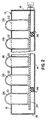
- FIG. 2 is a cross sectional side view of one embodiment of the video display.
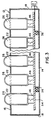
- FIG. 3 is a cross sectional side view of another embodiment of the video display.
- FIG. 1 illustrates a front elevational view of a preferred embodiment of a radio-frequency (RF) driven video display 10 which includes a plurality of electrodeless lamps 26.
- Video display 10 includes a box-shaped housing 12 defined by a back wall 14 and a front wall 16. Front wall 16 is spaced from back wall 14 by four side walls 18. The front, back and side walls may be made of a metal, such as aluminum.
- Front wall 16 contains a plurality of holes 20 formed therein. Each of the holes 20 is surrounded or defined by an adjacent cylindrical surface 22 formed in front wall 16.
- a conductive plate 34 electrically connected to an external RF generator 30, is preferably disposed within housing 12. The purpose of surface 22 and conductive plate 34 will be discussed later.
- Disposed within each of the holes 20 in front wall 16 and in proximity to a corresponding cylindrical surface 22 is an electrodeless lamp 26. As best shown in FIGS. 2 and 3, conductive plate 34 is positioned within proximity to one end of each of the lamps. The diameter of each hole is chosen slightly larger than the diameter of a respective lamp. The longitudinal axis of each lamp is arranged perpendicular to front wall 16.
- holes in the front wall are shown containing a lamp. In practice, all holes will contain an electrodeless lamp. Also, only a limited number (i.e., 81 in a 9 by 9 matrix) of holes or lamps is shown in FIG. 1. In actual practice, the display may contain many thousands of holes, with each one containing a lamp.
- a RF generator 30 provides RF energy to the interior of housing 12 through a 50 ohm connecting coaxial cable 32.
- the frequency of the power delivered to the housing is preferably from 10 to 100 megahertz.
- an impedance matching circuit which includes a tank circuit 38 consisting of a capacitor 40 and an inductive transformer 42 connected between RF generator 30 and lamps 26.
- a tank circuit 38 consisting of a capacitor 40 and an inductive transformer 42 connected between RF generator 30 and lamps 26.
- One end of capacitor 40 is connected to conductive plate 34 while the other end thereof is connected to one of the side walls 18.
- One end of transformer 42 is connected to the junction of capacitor 40 and conductive plate 34.
- the other end of transformer 42 is connected to one of the side walls 18.
- a tap winding on transformer 42 is connected by wire to the center contact of a conventional wall-mounted cable connector. The wire connecting the tap winding is electrically isolated from the side wall through which it extends.
- the external shell of the wall-mounted cable connector and the entire housing is electrically connected to ground.
- a suitable connector (shown in phanthom in FIGS. 2 and 3), which is connected to coaxial cable 32 (FIG. 1), mates with the wall-mounted connector.
- Tank circuit 38 matches the impedance of the RF generator to the impedance of the video display.
- capacitor 40 is variable so that tank circuit 38 can be tuned on a desirable resonant frequency.
- One suitable frequency is 40.68 megahertz.
- Each electrodeless lamp 26 is formed from a tubular envelope containing a fill material composed of a noble gas at low pressure and a quantity of mercury. Either the entire interior surface of the envelope or only that portion which extends external to the housing is coated with a suitable phosphor. Excitation of the fill material by a discharge within the envelope produces ultraviolet light which excites the phosphor coating to emit visible light at spectral regions governed by the composition of the phosphor.
- the RF energy provided by the RF generator 30 is capacitively coupled within housing 12 to each of the electrodeless lamps.
- the means for coupling the RF energy to the lamps includes the above mentioned cylindrical surface 22 in front wall 16 which surrounds each of the lamps together with conductive plate 34.
- conductive plate 34 is electrically isolated from back wall 14 by means of mounting insulators 36. Adequate spacing provides isolation of conductive plate 34 from front wall 16 and side walls 18.
- Conductive plate 34 provides an equipotential reference surface to RF to facilitate equal lamp energizing provided that its size is much smaller than the wavelength of the corresponding frequency.
- the conductive plate may be made of, for example, a solid sheet of metal, a metallic mesh screen or an insulative material having a metallized foil disposed thereon, such as, a copper-clad printed circuit board.
- the RF energy produces a strong electric field between the portion of the conductive plate in proximity to one end of a lamp and the cylindrical surface surrounding the lamp. This electric field is sufficient to cause breakdown and excitation of the electrodeless lamp fill material.
- the low pressure RF discharge produced in the lamp emits ultraviolet radiation which in turn is absorbed by the phosphor coating on the interior wall of the lamp and thereafter converted to visible light.
- all lamps in the video display are working in parallel. As a result, all lamps are illuminated together.
- a display can be used, for example, to display fixed images or text, either in black and white or color.
- the images or text are formed, for example, by lamps having a color different than the color of the remaining lamps which form the background.
- the displays can easily be changed by merely substituting or rearranging different colored lamps.
- the display can be used to provide backlighting for a liquid crystal display.
- a semiconductor switch 46 is coupled between conductive plate 34 and each of the lamps 26.
- the switches can be connected to a central control unit (not shown) which controls the operation of the individual lamps.
- a display which may be comprised of a large number of pixels, is useful in displaying, for example, moving text or television information.
- Each pixel is formed from a group of three electrodeless lamps with the grouped lamps of each pixel providing light sources at each of the primary colors, i.e., red, green and blue.
- the video display is constructed from a rectangular-shaped cast aluminum box 7.0 inches long, 7.0 inches wide and 2.5 inches deep.
- the front wall contains 54 holes arranged in a 6 by 9 matrix. Each hole contains an electrodeless lamp.
- a conductive plate 6.5 inches by 4.7 inches is disposed within the box and is isolated from the back wall by several insulators. The conductive plate is energized by RF power of about 100 volts at 40.68 megahertz.
- a matching tank circuit is disposed within the aluminum box and consists of an inductive transformer and a variable air capacitor. The transformer is constructed of four turns of 1 inch diameter from 1/8 inch copper tubing. A tap is provide between turns 1 and 2.
- the capacitor has a maximum capacitance of 25 picofarads.
- Each lamp is formed from 1/2 inch diameter tubing and has an overall length of 1 1/4 inches.
- a phosphor coating is disposed on the interior surface of each lamp.
- the lamps are filled with 100 percent argon at 3.0 torr and a quantity of mercury.
- the breakdown (i.e., starting) voltage of each lamp is from 75 to 80 volts.
- the lamps constructed in accordance with the teachings of the present invention do not possess the many limitations of lamps conventionally used with such displays. For example, burnout of an electrode can never be the cause of a failure of a lamp used in the present invention. Similarly, sputtering of electrode materials upon the surface of the phosphor, causing darkening thereof, is completely eliminated. Moreover, the problem of metal to glass or ceramic seals are completely eliminated. in addition, because of the electrodeless design, the cost and complexity of the wiring and socketing of the lamps is reduced. An added benefit to having a more reliable lamp is the reduced service cost which accompanies lamp replacement. Because the lack of electrodes eliminates end and cathode heating losses, the electrodeless RF lamps are more efficient than the regular fluorescent lamps used in in prior art displays.
Landscapes
- Physics & Mathematics (AREA)
- Engineering & Computer Science (AREA)
- Electromagnetism (AREA)
- Plasma & Fusion (AREA)
- General Physics & Mathematics (AREA)
- Theoretical Computer Science (AREA)
- Circuit Arrangements For Discharge Lamps (AREA)
- Devices For Indicating Variable Information By Combining Individual Elements (AREA)
- Discharge Lamps And Accessories Thereof (AREA)
Abstract
Claims (9)
- Moniteur vidéo d'affichage utilisant une énergie à haute fréquence pour illuminer des media luminescents, caractérisé par :
un boîtier métallique (12) défini par une paroi arrière (16) et une paroi frontale (16), la dite paroi frontale (16) étant séparée de la dite paroi arrière par des parois latérales (18), une pluralité d'orifices (20) étant définie dans la dite paroi frontale (16), chacun étant entouré par une surface cylindrique adjacente (22) formée sur la dite paroi frontale;
une pluralité de lampes dépourvues d'électrodes (26), chacune des dites lampes étant disposée à l'intérieur d'un orifice associé dans la dite paroi frontale;
un moyen à haute fréquente (30) pour délivrer une énergie à haute fréquence au dit boîtier; et
un moyen de couplage (22, 34) à l'intérieur du dit boîtier pour coupler l'énergie à haute fréquence émise par le dit moyen à haute fréquence aux dites lampes dépourvues d'électrodes, le dit moyen de couplage incluant la dite surface cylindrique (22) entourant chacune des dites lampes. - Moniteur vidéo d'affichage selon la revendication 1 caractérisé en ce que le dit moyen de couplage (22, 34) inclut, en outre, un moyen de plaque conductrice (34) disposé à l'intérieur des dites parois du dit boîtier et isolé de celles-ci, le dit moyen de plaque conductrice étant couplé au dit moyen à haute fréquence (30) de manière à déterminer une référence équipotentielle pour favoriser une alimentation égale des lampes.
- Moniteur vidéo d'affichage selon la revendication 2 caractérisé en ce que chacune des dites lampes (26) présente une extrémité à proximité du dit moyen de plaque conductrice (34).
- Moniteur vidéo d'affichage selon la revendication 2 comprenant, en outre, un moyen d'isolation pour isoler le dit moyen de plaque conductrice des dites parois du dit boîtier.
- Moniteur vidéo d'affichage selon la revendication 2 caractérisé en outre par un moyen de commutation (46) couplé entre le dit moyen de plaque conductrice (34) et chacune des dites lampes (26) pour déterminer une commande individuelle des lampes.
- Moniteur vidéo d'affichage selon la revendication 5 caractérisé en ce que le dit moyen de commutation inclut un commutateur semi-conducteur (46).
- Moniteur vidéo d'affichage selon l'une quelconque des revendications 1 à 6 caractérisé en ce que le dit moyen de couplage inclut, en outre, un moyen d'adaptation d'impédances (38) couplé entre le dit moyen à haute fréquence (30) et les dites lampes (26) pour adapter l'impédance du dit moniteur vidéo au dit moyen à haute fréquence.
- Moniteur vidéo d'affichage selon la revendication 7 caractérisé en ce que le dit moyen d'adaptation d'impédances inclut un circuit réservoir (38) comprenant un condensateur (40) et un transformateur inductif (42).
- Moniteur vidéo d'affichage selon la revendication 8 caractérisé en ce que le dit condensateur (40) est variable.
Applications Claiming Priority (3)
| Application Number | Priority Date | Filing Date | Title |
|---|---|---|---|
| US07/466,104 US5019750A (en) | 1990-01-16 | 1990-01-16 | Radio-frequency driven display |
| US466104 | 1990-01-16 | ||
| PCT/US1991/000285 WO1991010984A1 (fr) | 1990-01-16 | 1991-01-15 | Affichage commande par hautes frequences |
Publications (2)
| Publication Number | Publication Date |
|---|---|
| EP0511282A1 EP0511282A1 (fr) | 1992-11-04 |
| EP0511282B1 true EP0511282B1 (fr) | 1994-07-27 |
Family
ID=23850487
Family Applications (1)
| Application Number | Title | Priority Date | Filing Date |
|---|---|---|---|
| EP91903078A Expired - Lifetime EP0511282B1 (fr) | 1990-01-16 | 1991-01-15 | Affichage commande par hautes frequences |
Country Status (5)
| Country | Link |
|---|---|
| US (1) | US5019750A (fr) |
| EP (1) | EP0511282B1 (fr) |
| JP (1) | JPH05505248A (fr) |
| DE (1) | DE69103133T2 (fr) |
| WO (1) | WO1991010984A1 (fr) |
Families Citing this family (10)
| Publication number | Priority date | Publication date | Assignee | Title |
|---|---|---|---|---|
| US5325024A (en) * | 1992-10-16 | 1994-06-28 | Gte Products Corporation | Light source including parallel driven low pressure RF fluorescent lamps |
| US5619103A (en) * | 1993-11-02 | 1997-04-08 | Wisconsin Alumni Research Foundation | Inductively coupled plasma generating devices |
| US6433492B1 (en) * | 2000-09-18 | 2002-08-13 | Northrop Grumman Corporation | Magnetically shielded electrodeless light source |
| AUPS146502A0 (en) * | 2002-03-28 | 2002-05-09 | Traynor, Neil | Methods and apparatus relating to improved visual recognition and safety |
| FR2876495B1 (fr) * | 2004-10-11 | 2010-12-10 | Henri Bondar | Dispositif a influence electrique permettant l'ionisation d'un gaz a distance a travers une paroi isolante |
| DE102007057581A1 (de) * | 2007-11-28 | 2009-06-04 | Fachhochschule Aachen | Hochfrequenzlampe und Verfahren zu deren Betrieb |
| US8373352B2 (en) * | 2009-06-15 | 2013-02-12 | Topanga Technologies, Inc. | Electrodeless plasma lamp array |
| US8487544B2 (en) | 2010-09-29 | 2013-07-16 | Osram Sylvania Inc. | Power splitter circuit for electrodeless lamp |
| US11299405B2 (en) | 2017-09-28 | 2022-04-12 | Nxp Usa, Inc. | Purification apparatus with electrodeless bulb and methods of operation |
| US10475636B2 (en) | 2017-09-28 | 2019-11-12 | Nxp Usa, Inc. | Electrodeless lamp system and methods of operation |
Family Cites Families (16)
| Publication number | Priority date | Publication date | Assignee | Title |
|---|---|---|---|---|
| US2488169A (en) * | 1946-02-20 | 1949-11-15 | Benjamin B Schneider | Neon-type sign |
| US2566280A (en) * | 1949-03-31 | 1951-08-28 | Arthur F Yandt | Twin beam flashlight |
| US2920408A (en) * | 1956-09-17 | 1960-01-12 | Reed Res Inc | Electric display sign |
| US3500118A (en) * | 1967-07-17 | 1970-03-10 | Gen Electric | Electrodeless gaseous electric discharge devices utilizing ferrite cores |
| US3579015A (en) * | 1969-03-18 | 1971-05-18 | Monsanto Co | Electron beam addressed plasma display panel |
| US3629638A (en) * | 1970-01-15 | 1971-12-21 | Sperry Rand Corp | Plasma display device with internal-external electrode structure |
| US3997816A (en) * | 1975-04-21 | 1976-12-14 | Gte Laboratories Incorporated | Starting assist device for an electrodeless light source |
| JPS5293393A (en) * | 1976-02-02 | 1977-08-05 | Hitachi Ltd | High-frequency discharge spectrum light source |
| US4427921A (en) * | 1981-10-01 | 1984-01-24 | Gte Laboratories Inc. | Electrodeless ultraviolet light source |
| US4427920A (en) * | 1981-10-01 | 1984-01-24 | Gte Laboratories Incorporated | Electromagnetic discharge apparatus |
| FR2536563B1 (fr) * | 1982-11-23 | 1985-07-26 | Ssih Equipment Sa | Element emetteur de lumiere a tube a decharge pour tableau d'affichage matriciel |
| FR2559334B1 (fr) * | 1984-02-03 | 1988-02-26 | Ssih Equipment Sa | Dispositif d'alimentation pour commander l'intensite lumineuse d'au moins une lampe a decharge et utilisation dudit dispositif |
| US4647821A (en) * | 1984-09-04 | 1987-03-03 | Gte Laboratories Incorporated | Compact mercury-free fluorescent lamp |
| JPS61133551A (ja) * | 1984-12-03 | 1986-06-20 | Matsushita Electric Works Ltd | 螢光ランプ |
| AT388814B (de) * | 1985-11-15 | 1989-09-11 | Paar Anton Kg | Verfahren und vorrichtung zum erzeugen eines hf-induzierten edelgasplasmas |
| US5003233A (en) * | 1989-01-03 | 1991-03-26 | Gte Laboratories Incorporated | Radio frequency powered large scale display |
-
1990
- 1990-01-16 US US07/466,104 patent/US5019750A/en not_active Expired - Lifetime
-
1991
- 1991-01-15 EP EP91903078A patent/EP0511282B1/fr not_active Expired - Lifetime
- 1991-01-15 DE DE69103133T patent/DE69103133T2/de not_active Expired - Fee Related
- 1991-01-15 JP JP3503406A patent/JPH05505248A/ja active Pending
- 1991-01-15 WO PCT/US1991/000285 patent/WO1991010984A1/fr not_active Ceased
Also Published As
| Publication number | Publication date |
|---|---|
| DE69103133T2 (de) | 1995-03-09 |
| WO1991010984A1 (fr) | 1991-07-25 |
| US5019750A (en) | 1991-05-28 |
| DE69103133D1 (de) | 1994-09-01 |
| JPH05505248A (ja) | 1993-08-05 |
| EP0511282A1 (fr) | 1992-11-04 |
Similar Documents
| Publication | Publication Date | Title |
|---|---|---|
| US5325024A (en) | Light source including parallel driven low pressure RF fluorescent lamps | |
| US4559480A (en) | Color matrix display with discharge tube light emitting elements | |
| CA2069826C (fr) | Lampe a decharge et dispositif d'affichage d'images utilisant cette lampe et methode de fabrication de cette derniere | |
| US5027041A (en) | Integrated radio-frequency light source for large scale display | |
| US6316872B1 (en) | Cold cathode fluorescent lamp | |
| US6614185B1 (en) | Discharge tube with interior and exterior electrodes | |
| HU223365B1 (hu) | Eljárás világítórendszer üzemeltetésére és az ehhez alkalmas világítórendszer | |
| US5019750A (en) | Radio-frequency driven display | |
| US6201352B1 (en) | Cold cathode fluorescent display | |
| JPWO2000075961A1 (ja) | 放電ランプ、放電ランプ装置および読取装置 | |
| US7193363B2 (en) | Flat rare gas discharge lamp with variable output light color, illumination instrument comprising it, and its operating method | |
| US5003233A (en) | Radio frequency powered large scale display | |
| AU1316999A (en) | Gas discharge lamps and systems | |
| US5045754A (en) | Planar light source | |
| JP2003520387A (ja) | 冷陰極螢光灯(ランプ)およびディスプレイ | |
| US6337543B1 (en) | High power cold cathode gas discharge lamp using sub-electrode structures | |
| EP0635861B1 (fr) | Ecran luminescent pour dispositif d'affichage vidéo et son système de commande, et dispositif d'affichage vidéo à couleurs utilisant les mêmes | |
| US5977939A (en) | Gas flat display tube | |
| EP0948030A2 (fr) | Lampe à décharge à gaz rare, circuit d'éclairage et dispositif d'éclairage | |
| GB2050776A (en) | Cathode ray tube device for display systems | |
| KR100611033B1 (ko) | 코일 안테나를 갖는 형광 램프 및 이를 이용한 면광원 장치 | |
| JPH05190150A (ja) | 放電ランプ | |
| JPH0591254A (ja) | 照明装置 | |
| JPH04237943A (ja) | 面発光形光源装置およびその駆動方法 | |
| JPH05121048A (ja) | 照明装置 |
Legal Events
| Date | Code | Title | Description |
|---|---|---|---|
| PUAI | Public reference made under article 153(3) epc to a published international application that has entered the european phase |
Free format text: ORIGINAL CODE: 0009012 |
|
| 17P | Request for examination filed |
Effective date: 19920715 |
|
| AK | Designated contracting states |
Kind code of ref document: A1 Designated state(s): BE DE FR GB NL |
|
| 17Q | First examination report despatched |
Effective date: 19930906 |
|
| GRAA | (expected) grant |
Free format text: ORIGINAL CODE: 0009210 |
|
| AK | Designated contracting states |
Kind code of ref document: B1 Designated state(s): BE DE FR GB NL |
|
| REF | Corresponds to: |
Ref document number: 69103133 Country of ref document: DE Date of ref document: 19940901 |
|
| ET | Fr: translation filed | ||
| NLT1 | Nl: modifications of names registered in virtue of documents presented to the patent office pursuant to art. 16 a, paragraph 1 |
Owner name: OSRAM SYLVANIA INC. TE DANVERS, MASSACHUSETTS, VER |
|
| PLBE | No opposition filed within time limit |
Free format text: ORIGINAL CODE: 0009261 |
|
| STAA | Information on the status of an ep patent application or granted ep patent |
Free format text: STATUS: NO OPPOSITION FILED WITHIN TIME LIMIT |
|
| 26N | No opposition filed | ||
| PGFP | Annual fee paid to national office [announced via postgrant information from national office to epo] |
Ref country code: BE Payment date: 20001229 Year of fee payment: 11 |
|
| PGFP | Annual fee paid to national office [announced via postgrant information from national office to epo] |
Ref country code: GB Payment date: 20010111 Year of fee payment: 11 |
|
| PGFP | Annual fee paid to national office [announced via postgrant information from national office to epo] |
Ref country code: FR Payment date: 20010129 Year of fee payment: 11 |
|
| PGFP | Annual fee paid to national office [announced via postgrant information from national office to epo] |
Ref country code: NL Payment date: 20010131 Year of fee payment: 11 |
|
| PGFP | Annual fee paid to national office [announced via postgrant information from national office to epo] |
Ref country code: DE Payment date: 20010402 Year of fee payment: 11 |
|
| REG | Reference to a national code |
Ref country code: GB Ref legal event code: 732E |
|
| REG | Reference to a national code |
Ref country code: GB Ref legal event code: IF02 |
|
| PG25 | Lapsed in a contracting state [announced via postgrant information from national office to epo] |
Ref country code: GB Free format text: LAPSE BECAUSE OF NON-PAYMENT OF DUE FEES Effective date: 20020115 |
|
| PG25 | Lapsed in a contracting state [announced via postgrant information from national office to epo] |
Ref country code: BE Free format text: LAPSE BECAUSE OF NON-PAYMENT OF DUE FEES Effective date: 20020131 |
|
| BERE | Be: lapsed |
Owner name: GTE PRODUCTS CORP. Effective date: 20020131 |
|
| PG25 | Lapsed in a contracting state [announced via postgrant information from national office to epo] |
Ref country code: NL Free format text: LAPSE BECAUSE OF NON-PAYMENT OF DUE FEES Effective date: 20020801 Ref country code: DE Free format text: LAPSE BECAUSE OF NON-PAYMENT OF DUE FEES Effective date: 20020801 |
|
| GBPC | Gb: european patent ceased through non-payment of renewal fee |
Effective date: 20020115 |
|
| PG25 | Lapsed in a contracting state [announced via postgrant information from national office to epo] |
Ref country code: FR Free format text: LAPSE BECAUSE OF NON-PAYMENT OF DUE FEES Effective date: 20020930 |
|
| NLV4 | Nl: lapsed or anulled due to non-payment of the annual fee |
Effective date: 20020801 |
|
| REG | Reference to a national code |
Ref country code: FR Ref legal event code: ST |