EP0511511A2 - Mikroprozessorgesteuertes elektronisches Gerät - Google Patents
Mikroprozessorgesteuertes elektronisches Gerät Download PDFInfo
- Publication number
- EP0511511A2 EP0511511A2 EP92105658A EP92105658A EP0511511A2 EP 0511511 A2 EP0511511 A2 EP 0511511A2 EP 92105658 A EP92105658 A EP 92105658A EP 92105658 A EP92105658 A EP 92105658A EP 0511511 A2 EP0511511 A2 EP 0511511A2
- Authority
- EP
- European Patent Office
- Prior art keywords
- microprocessor
- mode
- category
- electronic equipment
- reset
- Prior art date
- Legal status (The legal status is an assumption and is not a legal conclusion. Google has not performed a legal analysis and makes no representation as to the accuracy of the status listed.)
- Granted
Links
Images


Classifications
-
- H—ELECTRICITY
- H04—ELECTRIC COMMUNICATION TECHNIQUE
- H04B—TRANSMISSION
- H04B1/00—Details of transmission systems, not covered by a single one of groups H04B3/00 - H04B13/00; Details of transmission systems not characterised by the medium used for transmission
- H04B1/38—Transceivers, i.e. devices in which transmitter and receiver form a structural unit and in which at least one part is used for functions of transmitting and receiving
- H04B1/40—Circuits
Definitions
- This invention relates, in general, to electronic equipment comprising microprocessors which incorporate an internal cache of (i) Random Access Memory (RAM) and (ii) Read Only Memory (ROM) and which have a capability of dual mode operation.
- RAM Random Access Memory
- ROM Read Only Memory
- This invention is particularly, but not exclusively, applicable to dual mode microprocessors associated with radio receiver circuits.
- Microprocessors are widely used in modern radio communications equipment. These microprocessors often form the basis for the control logic and communications circuitry within the radio and, in addition, of any other associated hardware.
- FIG. 1 illustrates a functional block diagram of a prior art radio.
- a receiver section 110 and a transmitter section 112 are shown as separate blocks.
- radios which operate in a simplex mode, wherein receive and transmit functions do not operate simultaneously often share components which are common to both circuits. This has a two-fold benefit: first, there is a reduction in the total number of components contained on the circuit board, and second, there is a corresponding reduction in the manufacturing cost.
- An external power source 111 such as a 12V battery in the case of a mobile radio transceiver, is coupled to a stabilised power supply 119. Outputs from this supply 120 are responsive to the receiver 110, the transmitter 112 and a processor 116.
- the outputs 120 of power supply 119 are d.c. (direct current) supplies, typically, +12V for RF (radio frequency) power circuits, + 10V for analog circuits and +5V for logic circuits.
- a first bidirectional signals bus 118 and a first bidirectional control bus 121 both comprising a plurality of conductors, couple the receiver 110 and the processor 116 together.
- the processor 116 is coupled to the transmitter 112 by a second signals bus 123 and a second controls bus 124.
- the second signals bus and the second controls bus both comprise a plurality of conductors.
- a third bidirectional bus 122 couples the processor 116 to a user interface 117.
- a loudspeaker 114 is coupled to a further output of the receiver 110.
- a microphone 115 is coupled to an additional input of the transmitter 112. Furthermore, the receiver 110 and the transmitter 112 are coupled to an antenna 113.
- the operational function of the receiver 110 can be summarised by the simplified steps of receiving a modulated RF (radio frequency) signal from the antenna 113, demodulating this received signal and finally relaying the information as an audio signal to the loud speaker 114.
- the operation of the transmitter 112 can be summarised by the steps of receiving an audio signal from the microphone 115, translating this information into a final modulated RF signal and then transmitting the modulated signal through the connected antenna 113.
- the processor can be seen to be comprised from a microprocessor 200, associated external ROM 201 and RAM 202 and interface circuitry 203, 204, 205.
- the processor also services the user interface 117.
- the user interface 117 comprises user input apparatus/circuitry, such as push buttons, selector switches and potentiometers, and user output displays, such as LCD's or LED indicators.
- a signals bus 207 which combines the first 118 and second 123 signals buses of figure 1, is coupled through an interface 205 to the microprocessor 200.
- a controls bus 208 which combines the first 121 and second 124 controls buses of figure 1, is coupled directly to the microprocessor 200, as is the third bidirectional bus 122.
- User interface 117 is responsive to the other end of the third bidirectional bus 122.
- An external crystal 206 provides a predetermined operating clock frequency for the microprocessor 200 and is coupled thereto.
- External ROM 201 and RAM 202 are coupled to the microprocessor 200 via an address bus 203 and a data bus 204.
- Microprocessor 200 is responsible for, among other things, the organisation of data flow between the various circuits in response to specific instructions, and for the timing of such data transfers.
- the microprocessor 200 has to output analog or digital signals to the receiver 110, the transmitter 112 and the user interface 117.
- the microprocessor 200 reads software programs stored in the ROM 201 and, occasionally, software programs stored in the RAM 202.
- the microprocessor 200 reads and writes information to data memory within the RAM 202.
- the software programs are constructed from modules of code, with each module related to specific operational functions of the radio.
- the modules of code which are operational at any one time are determined by the current states of the analog and digital signals from the receiver 110 and the transmitter 112, the current state of the radio (receiving or transmitting mode) and the user instructions obtained from the user interface 117.
- the rate of reading and writing information on the address bus 203 and the data bus 204 within the processor 116 is determined by the microprocessor's internal clock rate.
- the clock rate is derived from the external crystal 206.
- the crystal's frequency is 8MHz. This clock frequency equates to a corresponding read/write rate of 2MHz.
- microprocessor read/write operations on external busses causes the generation of a spectrum of noise spikes at the bus accessing frequency and at the n t " harmonics thereof. In the case of the MC68HC11, these noise spike occurs at 2MHz and at integer intervals of 2MHz.
- a microprocessor is running a (simple) program module which is, for example, accessed once every millisecond, then the 2MHz spectral noise components are widened by the frequency of the access rate i.e. ⁇ 1 kHz in the above example..
- Modern radio equipment operating at frequencies of 70-100MHz, often utilises fast software interrupt routines to generate and decode signalling data.
- This signalling data could be, for example, Motorola's proprietary Stat-Alert Digital Signalling Scheme or other standard signalling schemes such as the Select 5 tone signalling method (which is used widely across Europe and America) or the ZVEI Binary digital signalling method employed in Germany.
- the generated noise components can possess significant energies which affect the operational performance of the radio.
- the generated noise is transferred to the radio's sensitive receiver circuits 110 by capacitive and inductive pick-up from the address and data buses, direct radiation and by direct coupling through the signal and control busses.
- Another avenue which avails itself to the generated noise transfer process is the common power supply connection 120 (of figure 1) between circuit components.
- radio frequency (RF) signal strengths can be, for example, as low as 0.3uV.
- the generated noise pick-up is often an order of magnitude greater than this value (-3-5aV).
- the generated noise can therefore cause a significant and unacceptable reduction in the sensitivity of the radio and must be, in some way, eliminated, prevented or restricted.
- a second source of noise which requires consideration emanates from microprocessor driven equipment directly associated with the operation of the radio.
- This equipment could be a signalling unit for adding on signalling functions to a non-signalling radio.
- the associated equipment would be coupled to some, if not all, of the radio's connections e.g. the external power source 111, the signals bus 118 and the control bus 121, etc.
- This associated microprocessor driven equipment therefore contributes to the overall generation of noise within the system by the same mechanisms as described above.
- electronic equipment for example a radio receiver, which comprises a microprocessor.
- the microprocessor incorporates an on-chip memory and has the ability to operate in either a single chip mode or an expanded mode.
- the single chip mode restricts microprocessor operation to internal operation and thereby inhibits external addressing and locally generated noise, whereas the expanded mode allows external addressing.
- a software program comprised from modules of program code, is categorised into a first and a second category of routines.
- the first category of routines are stored in the internal memory and are related to equipment functions which are affected by generated noise to a higher degree (e.g. receive functions).
- the second category of routines are stored in the memory external to the microprocessor and are related to equipment functions which are affected by generated noise to a lesser degree (e.g. transmit functions). Furthermore, means are provided for executing the first category routines in the microprocessor's noise-limiting single chip mode and executing the second category routines in the microprocessor's expanded mode.
- the first category of routines are, additionally, sub-divided into primary and secondary algorithms.
- Primary first category algorithms comprise program code which is active continually.
- Secondary first category algorithms comprise code which is called upon from time to time but, when active, has a heavy bus usage. (This sub-division becomes necessary when the total code size of the first category routines exceeds the internal memory capacity of the microprocessor).
- the primary first category algorithms are permanently stored within the internal memory of the microprocessor while the secondary first category algorithms are, initially, stored in the external memory.
- the sub-division allows the use of an internal volatile memory.
- the secondary first category algorithms are only transferred to the internal on-chip memory of the microprocessor when required. Once loaded within the internal memory, the secondary algorithms are executed after the microprocessor has returned to the noise-limiting single chip mode.
- the microprocessor switches between the single chip mode and the expanded mode upon the reception of specific instructions. These instructions are either software or hardware generated and cause a mode change through the activation of a mode switch. Program control is maintained during a mode change by the use of an address or jump vector which is retained within either the internal memory of the microprocessor or in a storage means, such as a data latch.
- Electronic equipment so designed and described would therefore produce the novel advantages of a reduction in the amount of microprocessor generated noise and, in the application of the invention within radio receiver circuits, a corresponding improvement of the sensitivity therein. Furthermore, since the advantages obtained through the implementation of the invention are not based upon prior art techniques, additional advantages arise as a result of an associated reduction in the weight and size of the electronic equipment and a reduction in the overall complexity of implementation.
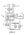
- Figure 3 illustrates a dual mode microprocessor 300 incorporated within a processor 116 of a prior art radio transceiver ( Figure 1).
- the dual mode microprocessor 300 comprises an internal cache of RAM 301 and ROM 302.
- the ROM 302 may be in the form of masked ROM or EPROM (Electrically Programmable ROM).
- the dual mode microprocessor may also contain EEPROM 303 (Electrically Erasable Programmable ROM) which can be used for either permanent program or data memory storage.
- EEPROM 303 Electrical Erasable Programmable ROM
- the dual mode microprocessor 300 functions in either a single chip mode or a expanded mode.
- the basic (normal) mode of operation occurs in the single chip mode wherein noise interference, which affects sensitive (radio receiver) functions and which is generated by external associated equipment and external bus accessing activity, is minimised.
- the microprocessor 300 is operating in this single chip mode, the external ROM 201 and RAM 202 are inoperative. Additionally, the external address bus 203 and data bus 204 are not energised. By rendering these external components and connections inactive, and by optimising the amount of time that the dual mode microprocessor 300 spends in internal operations, the amount of generated noise is substantially reduced.
- the desired reduction in the generated noise level within the sensitive (radio receive) functions of the radio is achieved and implemented through the partitioning of the program code within the dual mode microprocessor 300.
- Systematic analysis of the program code is used to relate each module of code to distinct operational functions of the radio. Since specific modules can be assigned to certain operational functions, two categories of code can therefore be derived.
- a first category of routines are involved with processor (radio) functions which are particularly susceptible to the affects of noise e.g. radio receiver functions. These first category routines are run inside the dual mode microprocessor 300 when the single chip mode is operative.
- Second category routines are involved with processor (radio) functions in which generated noise does not have such a dramatic effect on processor (radio) performance e.g.
- radio transmitting functions and functions which (a) change the mode of the equipment or (b) communicate with the user.
- These second category routines utilise the external memory 201, 202 and the external busses 118, 121, 203, 204 and are operative within the expanded mode.
- EEPROM 303 may also contain data constants which only change sporadically.
- present technology restricts internal microprocessor memory sizes. An internal masked ROM is typically -8K, whereas internal EEPROM, specifically in the case of Motorola's MC68HC11, has a memory size of up to 2K.
- the internal RAM 301 of the dual mode microprocessor 300 can be used to periodically store modules of first category routine code in addition to data and variables generated by the program.
- Internal RAM 301 is typically -0.5K.
- the first category routines may be further sub-divided into primary and secondary algorithms.
- the primary algorithms of the first category routines comprise program code which is active continually.
- Secondary algorithms comprise code which is called upon from time to time but, when active, has a heavy bus usage e.g. delay loops or loops which monitor for a change in state of an input, etc.
- the software is now arranged so that primary first category algorithms are stored permanently within the internal ROM (EPROM) 302 of the dual mode microprocessor 300, while secondary first category algorithms are initially stored in the external memory 201, 202. These secondary algorithms are transferred to the internal RAM 301 on a per call basis i.e. only when each specific routine is required. Once loaded within the internal RAM 301, the secondary algorithms are run when the dual mode microprocessor has returned it's noise limiting single chip mode.
- the microprocessor 300 switches between the single chip mode and the expanded mode upon the reception of specific instructions. These instructions are obtained as a result of any one of four kinds of event: (a) a program module operation; (b) a specified change in one of the signal 118 or control bus 121 lines; (c) a change in one of the user interface data output lines 305 initiated by a user; and, finally, (d) a change in the control input conductor 307, also initiated by the user.
- the mode change is performed through the activation of mode switch 308.
- a decoded, received data signal may require an acknowledgment in the form of a transmitted data message.
- the microprocessor generated noise is not significant in relation to any transmitted signal level. Therefore, any transmitted data acknowledgement can be processed and generated from program codes (modules) located in external ROM 201 and external RAM 202 i.e. within the expanded mode.
- a decoded, received data signal may instruct the dual mode microprocessor 300 to display the received information to the user.
- Another example of this type of initiated mode change occurs when, for example, analysis of the characteristics of the low level received signal is performed by external communications equipment.
- the analysed data is output through the user interface 117 to a peripheral user display.
- the expanded mode is initiated and program modules of code located in external ROM 201 will be accessed in order to generate a desired user display output.
- the second kind of event resulting in a mode change (b), relates to a specific change in one of the signal 118 or control bus 121 lines, is primarily concerned with set up procedures for the radio.
- a radio receiver may contain hardware for identifying and detecting a received signal. This hardware could be based on, for example, the detection of the modulating carrier wave of the received signal.
- the receiver Upon the detection of an incoming signal, the receiver provides a control line change to the dual mode microprocessor 300.
- the dual mode microprocessor then alerts the user that an incoming call has been received. This could typically be performed by either illuminating a "CALL" indicator or by generating a tone through the radio's audio speaker 114 or both.
- the expanded mode can once again be utilised wherein program code stored within the external ROM 201 is accessed.
- a key such as a push to talk (PTT) key
- PTT push to talk
- the user may select a change channel key such as a Mode Select or Scan key (not shown), whereupon the radio's operating mode is changed to the expanded mode.
- PTT push to talk
- Scan key not shown
- These user key inputs may be coupled directly to the dual mode microprocessor 300 through one of the data outputs 306 or via the control input conductor 307. An input to the microprocessor via the control conductor 307 would, typically, require the microprocessor to ascertain which user key had been activated.
- an address or jump vector is written into the internal RAM of the dual mode microprocessor.
- This address or jump vector retains program control during the mode change.
- the address or vector points to a specific start location of a desired routine which is to be initiated after the micro-reset has been forced.
- This address or vector is stored within the internal RAM because the contents of this memory are conserved during the micro-reset.
- each type of reset used by the dual mode microprocessor e.g. clock monitor fail, illegal op-code, watchdog timer time out or an electrical reset, has a unique reset address or vector.
- a simple routine executes a JUMP command to a program segment specified by the stored RAM address or vector. Since a micro-reset clears certain microprocessor registers and ports, the first procedure initiated by the program segment after a mode change has occurred is the re-initialisation of these registers and ports.
- an external serial or parallel data latch (not shown) can be loaded with a bit value which represents a specific start location. This external latch can be read after the mode change to order to obtain the desired jump vector.
- an 8- bit serial latch can be loaded with 2 8 possible states. Each state therefore maps to one of 2 8 different program segments. It should be appreciated by one skilled in the art that other forms of storage devices, which retain data, can also be used e.g. a parallel data latch or a first-in-first-out (fifo) memory.
- All dual mode microprocessors 300 have one or more mode inputs which define their operating mode.
- the logic states of two input pins determine the operating mode.
- the expanded mode is obtained by switching the MODEA input from a low logic value to a high logic value.
- MODEB is permanently tied through a resistor to a value of +5V.
- these inputs are read by the dual mode microprocessor 300 after a reset signal has been received.
- the operating mode is changed by, first, configuring the mode input(s) for the new, specified operating mode and, second, by forcing a microprocessor reset.
- microprocessor micro-reset There are two alternative techniques by which a microprocessor micro-reset can be performed. These are: a software initiated reset and a hardware initiated reset.
- Modern dual mode microprocessors 300 normally contain an internal hardware circuit which verifies the presence and operation of the microprocessor's internal clock. In the absence of the internal clock signal, this internal hardware circuit forces a micro-reset. Therefore, this clock monitor fail provides a first method of changing modes.
- the clock monitor enable (CME) bit in the CONFIG register is enabled and the stop disable (S) bit in the CCR register is cleared. The mode change then occurs when a STOP instruction is issued from the software.
- the clock monitor reset is guaranteed and is automatically forced after a delay of between 5 and 100 microseconds (us) This delay time is set by an internal RC circuit contained within the microprocessor.
- the program code In order to reset the COP timer within the microprocessor, the program code must write contiguous hexadecimal instructions $55 and $AA to the COPRST register within a time interval smaller than the COP timer period.
- These reset instructions are implemented by either a program segment within a major software program loop/execution or by an interrupt routine which is independent of the main program loop.
- the reset instruction is activated every 10ms of the MC68HC11's internal software timers. It can therefore be appreciated that a mode change can also be initiated, when required, by stopping the reset of the COP timer i.e. by producing a watchdog timer time-out.
- the COP reset and hence a micro-reset will automatically be forced within a period of 16.384ms.
- the exact time period before reset is determined by the defined COP time-out and by the length of time that has elapsed since the previous COP timer reset.
- a third method of forcing a software initiated micro-reset is through the use of an illegal Op-code detect circuit.
- modern dual mode microprocessors often contain internal hardware circuits which specifically check the software program code for undefined or illegal op-code instructions.
- a micro-reset is forced if, for example, the microprocessor receives a program data value instead of an expected instruction op-code. Therefore, a mode change can be instigated, when required, by the issuance of a BRANCH or JUMP instruction, from the software, to a code address containing a computational constant. This location must contain a constant which does not signify a legal op-code for the dual mode microprocessor. Any discovered illegal op-code will, consequentially, cause an immediate forced micro-reset.
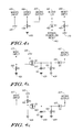
- FIG. 4a A hardware method for forcing a micro-reset in a dual mode microprocessor with an active low input pin e.g. the Motorola MC68HC11, is illustrated in figure 4a.
- An active low reset input 400 and a bidirectional input/output pin 401 of the dual mode microprocessor 300 are coupled together.
- a power-up reset signal 402 is coupled through the negative terminal of a diode 403 to the bidirectional input/output pin 401.
- This reset signal 402 is provided by modern microprocessor equipment so as to maintain a reset mode within the processor immediately after power-up has occurred.
- This power-up reset mode remains active until the +5V power supply to the logic reaches a preset minimum value, typically +4.75V, at which point the processor is guaranteed to function correctly.
- the reset pin 400 is coupled through a pull-up resistor 404 to the +5V power supply voltage 120.
- bidirectional input/output pin 401 operates as an input and the power-up reset input 402 is high ( + 5V).
- the voltage drop across resistor 404 ties the reset pin 400 to the +5V supply and ensures that the reset signal 402 is removed from the microprocessor. Operation of the microprocessor then commences.
- Bidirectional input/output pin 401 operates as an input and, as a result of the action of diode 403, the reset input pin 400 is pulled low.
- mode input pin MODEB 405 is tied through a resistor (not shown) to the +5V supply 120.
- the MODEA input 406 is coupled to a microprocessor output 407 and, additionally, to ground (0V) potential 409 through pull-down resistor 408.
- Microprocessor output 407 is any general purpose output pin provided by the microprocessor. Therefore, since the output pin 407 is low after a micro-reset has been forced, MODEA input 406 is also low and the single-chip mode is obtained upon power-up.
- a mode change can be initiated, when required, by first setting the micro output 407 to the designated logic state which determines the operating mode and then, second, changing the bidirectional input/output pin 401 to an output with a low logic level.
- a hardware initiated micro-reset now occurs. It should be apparent that, in the case of the Motorola MC68HC11, the logic state of the MODEA pin on micro-reset determines the operating mode of the dual mode microprocessor.
- the bidirectional input/output pin 401 only remains as an output until the dual mode microprocessor has started its reset routine. By automatically resuming its input function, the input/output pin 401 ensures that the microprocessor only remains in a reset state for the minimal length of time.
- resistor 404 in order to reverse the operating polarity of the dual mode microprocessor reset, resistor 404 would be coupled to ground potential (thereby acting as a pull-down resistor) and diode 403 would be orientated with a reversed polarity.
- Figure 4a illustrates the preferred embodiment of the hardware mode switch (308 of figure 3) for a dual mode microprocessor 300, such as Motorola's MC68HC11, which requires only one mode input change to facilitate a mode switch.
- a dual mode microprocessor requires a mode input pin to be set at a high logic level upon power-up and then changed to a low logic level during operation, the mode input pin should be coupled to a bidirectional input/output pin in an identical manner to that described for the power-up reset pin.
- resistor 408 should act as a pull-up resistor and should therefore be coupled to the +5V supply 120.
- each mode input pin must be coupled to an output pin.
- This output pin can be any one of the general purpose output pins provided by the microprocessor.
- dual mode microprocessors often read their mode input pins immediately on a micro-reset instruction and before the initialization of microprocessor output pins occurs. Therefore, the output states for the required new mode are set before the forced micro-reset.
- FIG. 4b and 4c illustrate hardware configurations capable of producing finite hold times.
- FIG. 4b illustrates a finite hold time circuit specifically supplying low input conditions to a microprocessor mode select input pin 417 on initial power-up.
- Micro output 407 is coupled through diode 415 to the gate terminal of a p-channel JFET 410.
- a 5V voltage supply 120 is coupled to the source terminal of the JFET 410 and a drain terminal is coupled to the mode input 417.
- a resistor 418 is coupled between the mode input 417 and ground 409.
- a parallel combination of a capacitor 411 and a resistor 414 are coupled between ground 409 and the gate of the JFET and the negative terminal of the diode 415. Resistor 418 holds mode input 417 at a low logic level.
- the microprocessor output pin 407 is low.
- the JFET will be nonconducting and the input state of the mode input determined by resistor 418.
- the micro output pin 407 is set high. This causes the JFET to become conducting and therefore sets the mode input pin 417 to a high logic state. After a micro-reset has been forced, the micro output pin 407 returns to a low logic level without affecting the the operation of the JFET 410.
- the JFET remains on because diode 415 prevents capacitor 411 from discharging.
- the time constant produced by the product of the capacitance of capacitor 411 and the resistance of resistor 414 therefore determines the time duration for which the mode input pin 417 remains at a high logic level.
- Figure 4c illustrates a finite hold time circuit specifically supplying high input conditions to a microprocessor mode select input pin 417 on initial power-up.
- the time duration that the mode input pin remains high is again determined by the time constant generated by the previously described parallel, open circuited RC configuration.
- Micro output 407 is coupled through diode 415 to the gate terminal of p-channel JFET 410.
- mode input 417 is coupled to the source terminal of JFET 410.
- mode input 417 is coupled to the +5V voltage supply 120 through resistor 416.
- the drain terminal of JFET 410 is coupled to ground (0V) potential 409.
- resistor 416 holds mode input 417 at a high logic level.
- Dual mode microprocessor control bus lines (121 of figure 3) which control the radio components, such as the transmitter and receiver, must retain their logic states during a mode change. Normally, all output lines from a dual mode microprocessor are set to a low logic level after a micro-reset has occurred. However, when the dual mode microprocessor is operating in the single chip mode, certain input lines are required to operate at high logic levels e.g. the PTT input on a conventional radio is normally at a high logic level when in a radio receive mode. These high input states in the single chip mode can be obtained through the use of either parallel or serial data latches or pull-up resistors in conjunction with bidirectional input/output lines.
- a supplementary advantage derived from the use of bidirectional input/output lines is that these lines can be defined as additional outputs in the expanded mode. After a micro-reset has been forced, any line which has been defined as an output automatically reverts back to an input, with its logic state determined by the associated pull-up or pull-down resistor.
- the preferred embodiment of the invention is particularly, but not exclusively, applicable to an application within radio equipment. Furthermore, an application for the invention can be found within "add-on" equipment which is external to the radio but which has a tendency to generate RF noise. However, it should be obvious to one skilled in the art that the invention could as equally well be applied to any multi-mode electronic apparatus wherein a first mode is sensitive to microprocessor generated noise e.g. spectrum analysers and communications test equipment.
- an invention so designed and described would produce the novel advantages of a reduction in the amount of microprocessor generated noise and, consequentially, an improvement in the sensitivity of (i) the microprocessor and, more importantly, (ii) any associated radio receiver. Furthermore, there is an additional reduction in the overall cost of a radio receiver which encompasses this invention. In addition, further benefits are derived from a reduction in weight and size of a radio and a reduction in the complexity of implementation.
Landscapes
- Computer Networks & Wireless Communication (AREA)
- Signal Processing (AREA)
- Engineering & Computer Science (AREA)
- Noise Elimination (AREA)
- Transceivers (AREA)
- Selective Calling Equipment (AREA)
- Massaging Devices (AREA)
- Electrophonic Musical Instruments (AREA)
- Computer And Data Communications (AREA)
- Liquid Crystal Substances (AREA)
- Glass Compositions (AREA)
- Sheets, Magazines, And Separation Thereof (AREA)
- Radar Systems Or Details Thereof (AREA)
- Circuits Of Receivers In General (AREA)
- Microcomputers (AREA)
Applications Claiming Priority (2)
| Application Number | Priority Date | Filing Date | Title |
|---|---|---|---|
| GB919109301A GB9109301D0 (en) | 1991-04-30 | 1991-04-30 | Electronic equipment |
| GB9109301 | 1991-04-30 |
Publications (3)
| Publication Number | Publication Date |
|---|---|
| EP0511511A2 true EP0511511A2 (de) | 1992-11-04 |
| EP0511511A3 EP0511511A3 (en) | 1993-05-12 |
| EP0511511B1 EP0511511B1 (de) | 1996-12-11 |
Family
ID=10694203
Family Applications (1)
| Application Number | Title | Priority Date | Filing Date |
|---|---|---|---|
| EP92105658A Expired - Lifetime EP0511511B1 (de) | 1991-04-30 | 1992-04-02 | Mikroprozessorgesteuertes elektronisches Gerät |
Country Status (6)
| Country | Link |
|---|---|
| US (1) | US5404547A (de) |
| EP (1) | EP0511511B1 (de) |
| JP (1) | JP2748773B2 (de) |
| AT (1) | ATE146317T1 (de) |
| DE (1) | DE69215744T2 (de) |
| GB (1) | GB9109301D0 (de) |
Cited By (16)
| Publication number | Priority date | Publication date | Assignee | Title |
|---|---|---|---|---|
| WO1995001675A1 (en) * | 1993-07-01 | 1995-01-12 | Motorola, Inc. | Expanded microcomputer system for controlling radio frequency interference |
| WO1997008839A3 (en) * | 1995-08-31 | 1997-05-22 | Northrop Grumman Corp | Digitally programmable multifunction radio system architecture |
| US5859878A (en) * | 1995-08-31 | 1999-01-12 | Northrop Grumman Corporation | Common receive module for a programmable digital radio |
| US5867535A (en) * | 1995-08-31 | 1999-02-02 | Northrop Grumman Corporation | Common transmit module for a programmable digital radio |
| US5909193A (en) * | 1995-08-31 | 1999-06-01 | Northrop Grumman Corporation | Digitally programmable radio modules for navigation systems |
| FR2857111A1 (fr) * | 2003-07-02 | 2005-01-07 | St Microelectronics Sa | Microcontroleur a protection logique contre les decharges electrostatiques |
| US6923701B2 (en) | 2001-11-14 | 2005-08-02 | Polydisplay Asa | Display with micro pockets |
| US7414560B2 (en) | 2005-06-29 | 2008-08-19 | Shaojie Chen | Wireless communication system including an audio underflow protection mechanism operative with time domain isolation |
| US7433393B2 (en) | 2004-07-23 | 2008-10-07 | Nxp B.V. | Apparatus for controlling a digital signal processor for radio isolation and associated methods |
| US7567637B2 (en) | 2004-09-30 | 2009-07-28 | St-Ericsson Sa | Wireless communication system and method with frequency burst acquisition feature using autocorrelation and narrowband interference detection |
| US7593482B2 (en) | 2004-09-30 | 2009-09-22 | St-Ericsson Sa | Wireless communication system with hardware-based frequency burst detection |
| US7761056B2 (en) | 2004-07-23 | 2010-07-20 | St-Ericsson Sa | Method of controlling a processor for radio isolation using a timer |
| US7805170B2 (en) | 2005-03-30 | 2010-09-28 | St-Ericsson Sa | System and method for efficient power supply regulation compatible with radio frequency operation |
| US7864891B2 (en) | 2005-12-20 | 2011-01-04 | Silicon Laboratories Inc. | Method and apparatus for acquiring a frequency burst in a radio communication device |
| US8884791B2 (en) | 2004-06-29 | 2014-11-11 | St-Ericsson Sa | Keypad scanning with radio event isolation |
| CN105899955A (zh) * | 2013-12-30 | 2016-08-24 | 德克萨斯仪器股份有限公司 | 基于差分/不对称的感应感测的齿轮感测 |
Families Citing this family (44)
| Publication number | Priority date | Publication date | Assignee | Title |
|---|---|---|---|---|
| US4807975A (en) * | 1985-04-17 | 1989-02-28 | Masataka Negishi | Image forming system having uniform illumination flux for liquid crystal image means |
| DE69228980T2 (de) * | 1991-12-06 | 1999-12-02 | National Semiconductor Corp., Santa Clara | Integriertes Datenverarbeitungssystem mit CPU-Kern und unabhängigem parallelen, digitalen Signalprozessormodul |
| US5557743A (en) * | 1994-04-05 | 1996-09-17 | Motorola, Inc. | Protection circuit for a microprocessor |
| JP4312272B2 (ja) * | 1995-10-06 | 2009-08-12 | モトローラ・インコーポレイテッド | 内部メモリへのアクセスを制限するマイクロコントローラ |
| US5737760A (en) * | 1995-10-06 | 1998-04-07 | Motorola Inc. | Microcontroller with security logic circuit which prevents reading of internal memory by external program |
| US5907580A (en) * | 1996-06-10 | 1999-05-25 | Morphics Technology, Inc | Method and apparatus for communicating information |
| US6724833B1 (en) * | 1996-06-10 | 2004-04-20 | Infineon Technologies Ag | Method and apparatus for communicating information |
| JPH11338716A (ja) | 1998-05-29 | 1999-12-10 | Nec Corp | 無線端末、及び無線端末における受信方法 |
| JP3241332B2 (ja) | 1998-10-27 | 2001-12-25 | 日本電気株式会社 | 無線携帯端末のノイズ低減方法 |
| JP4177525B2 (ja) | 1999-07-23 | 2008-11-05 | 京セラ株式会社 | 携帯電話機 |
| JP2003018030A (ja) * | 2001-06-29 | 2003-01-17 | Niigata Seimitsu Kk | 受信機 |
| US7290161B2 (en) * | 2003-03-24 | 2007-10-30 | Intel Corporation | Reducing CPU and bus power when running in power-save modes |
| US8019382B2 (en) * | 2004-12-29 | 2011-09-13 | St-Ericsson Sa | Communication apparatus having a standard serial communication interface compatible with radio isolation |
| US7209061B2 (en) | 2005-03-30 | 2007-04-24 | Silicon Laboratories, Inc. | Method and system for sampling a signal |
| US8854019B1 (en) | 2008-09-25 | 2014-10-07 | Rf Micro Devices, Inc. | Hybrid DC/DC power converter with charge-pump and buck converter |
| US9166471B1 (en) | 2009-03-13 | 2015-10-20 | Rf Micro Devices, Inc. | 3D frequency dithering for DC-to-DC converters used in multi-mode cellular transmitters |
| US8315576B2 (en) | 2009-05-05 | 2012-11-20 | Rf Micro Devices, Inc. | Capacitive compensation of cascaded directional couplers |
| US8548398B2 (en) | 2010-02-01 | 2013-10-01 | Rf Micro Devices, Inc. | Envelope power supply calibration of a multi-mode radio frequency power amplifier |
| US8538355B2 (en) | 2010-04-19 | 2013-09-17 | Rf Micro Devices, Inc. | Quadrature power amplifier architecture |
| US9008597B2 (en) | 2010-04-20 | 2015-04-14 | Rf Micro Devices, Inc. | Direct current (DC)-DC converter having a multi-stage output filter |
| US8983410B2 (en) | 2010-04-20 | 2015-03-17 | Rf Micro Devices, Inc. | Configurable 2-wire/3-wire serial communications interface |
| US9900204B2 (en) * | 2010-04-20 | 2018-02-20 | Qorvo Us, Inc. | Multiple functional equivalence digital communications interface |
| US8811921B2 (en) | 2010-04-20 | 2014-08-19 | Rf Micro Devices, Inc. | Independent PA biasing of a driver stage and a final stage |
| US8842399B2 (en) | 2010-04-20 | 2014-09-23 | Rf Micro Devices, Inc. | ESD protection of an RF PA semiconductor die using a PA controller semiconductor die |
| US9030256B2 (en) | 2010-04-20 | 2015-05-12 | Rf Micro Devices, Inc. | Overlay class F choke |
| US9362825B2 (en) | 2010-04-20 | 2016-06-07 | Rf Micro Devices, Inc. | Look-up table based configuration of a DC-DC converter |
| US9553550B2 (en) | 2010-04-20 | 2017-01-24 | Qorvo Us, Inc. | Multiband RF switch ground isolation |
| US8831544B2 (en) | 2010-04-20 | 2014-09-09 | Rf Micro Devices, Inc. | Dynamic device switching (DDS) of an in-phase RF PA stage and a quadrature-phase RF PA stage |
| US8913971B2 (en) | 2010-04-20 | 2014-12-16 | Rf Micro Devices, Inc. | Selecting PA bias levels of RF PA circuitry during a multislot burst |
| US8942651B2 (en) | 2010-04-20 | 2015-01-27 | Rf Micro Devices, Inc. | Cascaded converged power amplifier |
| US8947157B2 (en) | 2010-04-20 | 2015-02-03 | Rf Micro Devices, Inc. | Voltage multiplier charge pump buck |
| US9184701B2 (en) | 2010-04-20 | 2015-11-10 | Rf Micro Devices, Inc. | Snubber for a direct current (DC)-DC converter |
| US9577590B2 (en) | 2010-04-20 | 2017-02-21 | Qorvo Us, Inc. | Dual inductive element charge pump buck and buck power supplies |
| US9214865B2 (en) | 2010-04-20 | 2015-12-15 | Rf Micro Devices, Inc. | Voltage compatible charge pump buck and buck power supplies |
| US8989685B2 (en) | 2010-04-20 | 2015-03-24 | Rf Micro Devices, Inc. | Look-up table based configuration of multi-mode multi-band radio frequency power amplifier circuitry |
| US9077405B2 (en) | 2010-04-20 | 2015-07-07 | Rf Micro Devices, Inc. | High efficiency path based power amplifier circuitry |
| US8942650B2 (en) | 2010-04-20 | 2015-01-27 | Rf Micro Devices, Inc. | RF PA linearity requirements based converter operating mode selection |
| US9048787B2 (en) | 2010-04-20 | 2015-06-02 | Rf Micro Devices, Inc. | Combined RF detector and RF attenuator with concurrent outputs |
| US8983407B2 (en) | 2010-04-20 | 2015-03-17 | Rf Micro Devices, Inc. | Selectable PA bias temperature compensation circuitry |
| US9214900B2 (en) | 2010-04-20 | 2015-12-15 | Rf Micro Devices, Inc. | Interference reduction between RF communications bands |
| US8958763B2 (en) | 2010-04-20 | 2015-02-17 | Rf Micro Devices, Inc. | PA bias power supply undershoot compensation |
| US8892063B2 (en) | 2010-04-20 | 2014-11-18 | Rf Micro Devices, Inc. | Linear mode and non-linear mode quadrature PA circuitry |
| US8811920B2 (en) | 2010-04-20 | 2014-08-19 | Rf Micro Devices, Inc. | DC-DC converter semiconductor die structure |
| US9065505B2 (en) | 2012-01-31 | 2015-06-23 | Rf Micro Devices, Inc. | Optimal switching frequency for envelope tracking power supply |
Family Cites Families (3)
| Publication number | Priority date | Publication date | Assignee | Title |
|---|---|---|---|---|
| JPH0642691B2 (ja) * | 1988-05-21 | 1994-06-01 | 富士通株式会社 | 移動電話端末 |
| JPH0744477B2 (ja) * | 1988-07-15 | 1995-05-15 | 日本電気株式会社 | 小型デジタル無線受信機 |
| US5020093A (en) * | 1989-06-23 | 1991-05-28 | Motorola, Inc. | Cellular telephone operable on different cellular telephone systems |
-
1991
- 1991-04-30 GB GB919109301A patent/GB9109301D0/en active Pending
-
1992
- 1992-04-02 AT AT92105658T patent/ATE146317T1/de not_active IP Right Cessation
- 1992-04-02 EP EP92105658A patent/EP0511511B1/de not_active Expired - Lifetime
- 1992-04-02 DE DE69215744T patent/DE69215744T2/de not_active Expired - Fee Related
- 1992-04-27 JP JP4131457A patent/JP2748773B2/ja not_active Expired - Fee Related
- 1992-04-29 US US07/875,930 patent/US5404547A/en not_active Expired - Fee Related
Cited By (21)
| Publication number | Priority date | Publication date | Assignee | Title |
|---|---|---|---|---|
| WO1995001675A1 (en) * | 1993-07-01 | 1995-01-12 | Motorola, Inc. | Expanded microcomputer system for controlling radio frequency interference |
| US5471663A (en) * | 1993-07-01 | 1995-11-28 | Motorola, Inc. | Expanded microcomputer system for controlling radio frequency interference |
| AU668835B2 (en) * | 1993-07-01 | 1996-05-16 | Motorola, Inc. | Expanded microcomputer system for controlling radio freqfrequency interference |
| WO1997008839A3 (en) * | 1995-08-31 | 1997-05-22 | Northrop Grumman Corp | Digitally programmable multifunction radio system architecture |
| US5859878A (en) * | 1995-08-31 | 1999-01-12 | Northrop Grumman Corporation | Common receive module for a programmable digital radio |
| US5867535A (en) * | 1995-08-31 | 1999-02-02 | Northrop Grumman Corporation | Common transmit module for a programmable digital radio |
| US5909193A (en) * | 1995-08-31 | 1999-06-01 | Northrop Grumman Corporation | Digitally programmable radio modules for navigation systems |
| AU713098B2 (en) * | 1995-08-31 | 1999-11-25 | Gec-Marconi Hazeltine Corporation | Digitally programmable multifunction radio system architecture |
| US6072994A (en) * | 1995-08-31 | 2000-06-06 | Northrop Grumman Corporation | Digitally programmable multifunction radio system architecture |
| US6923701B2 (en) | 2001-11-14 | 2005-08-02 | Polydisplay Asa | Display with micro pockets |
| FR2857111A1 (fr) * | 2003-07-02 | 2005-01-07 | St Microelectronics Sa | Microcontroleur a protection logique contre les decharges electrostatiques |
| US8884791B2 (en) | 2004-06-29 | 2014-11-11 | St-Ericsson Sa | Keypad scanning with radio event isolation |
| US7433393B2 (en) | 2004-07-23 | 2008-10-07 | Nxp B.V. | Apparatus for controlling a digital signal processor for radio isolation and associated methods |
| US7761056B2 (en) | 2004-07-23 | 2010-07-20 | St-Ericsson Sa | Method of controlling a processor for radio isolation using a timer |
| US7567637B2 (en) | 2004-09-30 | 2009-07-28 | St-Ericsson Sa | Wireless communication system and method with frequency burst acquisition feature using autocorrelation and narrowband interference detection |
| US7593482B2 (en) | 2004-09-30 | 2009-09-22 | St-Ericsson Sa | Wireless communication system with hardware-based frequency burst detection |
| US7805170B2 (en) | 2005-03-30 | 2010-09-28 | St-Ericsson Sa | System and method for efficient power supply regulation compatible with radio frequency operation |
| US7414560B2 (en) | 2005-06-29 | 2008-08-19 | Shaojie Chen | Wireless communication system including an audio underflow protection mechanism operative with time domain isolation |
| US7864891B2 (en) | 2005-12-20 | 2011-01-04 | Silicon Laboratories Inc. | Method and apparatus for acquiring a frequency burst in a radio communication device |
| CN105899955A (zh) * | 2013-12-30 | 2016-08-24 | 德克萨斯仪器股份有限公司 | 基于差分/不对称的感应感测的齿轮感测 |
| CN105899955B (zh) * | 2013-12-30 | 2020-07-10 | 德克萨斯仪器股份有限公司 | 基于差分/不对称的感应感测的齿轮感测 |
Also Published As
| Publication number | Publication date |
|---|---|
| US5404547A (en) | 1995-04-04 |
| EP0511511B1 (de) | 1996-12-11 |
| GB9109301D0 (en) | 1991-06-19 |
| DE69215744D1 (de) | 1997-01-23 |
| DE69215744T2 (de) | 1997-06-12 |
| ATE146317T1 (de) | 1996-12-15 |
| JPH05158821A (ja) | 1993-06-25 |
| EP0511511A3 (en) | 1993-05-12 |
| JP2748773B2 (ja) | 1998-05-13 |
Similar Documents
| Publication | Publication Date | Title |
|---|---|---|
| EP0511511B1 (de) | Mikroprozessorgesteuertes elektronisches Gerät | |
| US5604928A (en) | Portable electronic device with radio communication and controlled computer status | |
| US5862405A (en) | Peripheral unit selection system having a cascade connection signal line | |
| EP0329725B1 (de) | Mikrorechner mit eingebauter chipauswahl und programmierbarer busdehnung | |
| EP0619548A1 (de) | Für zwei verschiedene Protokollstandards geeignete Schnittstellenschaltung zwischen einem Steuerbus und einer integrierten Schaltung | |
| WO1996037851A1 (en) | Serial interface capable of operating in two different serial data transfer modes | |
| GB2304259B (en) | Radio apparatus suitable for use with an information processor | |
| US4967108A (en) | Differential-time-constant bandpass filter using the analog properties of digital circuits | |
| US4972184A (en) | Polling system for use in an audio system | |
| US5059836A (en) | Differential-time-constant bandpass filter using the analog properties of digital circuits | |
| KR920005168A (ko) | 테스트 모드 동안의 출력 동작으로부터 칩 동작 제어를 가진 반도체 메모리 | |
| US5805904A (en) | Power control circuit of at least one computer expansion slot | |
| US5604916A (en) | Controlling device for switching serial communication port and light communication port and its driving method | |
| US6052746A (en) | Integrated circuit having programmable pull device configured to enable/disable first function in favor of second function according to predetermined scheme before/after reset | |
| CN220121165U (zh) | 控制电路、装置及芯片 | |
| US5012404A (en) | Integrated circuit remote terminal stores interface for communication between CPU and serial bus | |
| US5838073A (en) | Sideband communication on the standard parallel SCSI bus | |
| US5918066A (en) | Method and device for displaying configuration information of a computer through a speaker output port of the computer | |
| US6530048B1 (en) | I2C test single chip | |
| US5938746A (en) | System for prioritizing slave input register to receive data transmission via bi-directional data line from master | |
| US6680631B2 (en) | Setting the speed of clocked circuitry | |
| KR100256944B1 (ko) | 피씨아이 핫 플러그를 위한 경보 장치 | |
| JP2854194B2 (ja) | マイクロコンピュータの発振クロック判定装置 | |
| US20250251865A1 (en) | Memory device, memory system, and operating method of the memory device | |
| Mitchell et al. | An integrated serial bus architecture: principles and applications |
Legal Events
| Date | Code | Title | Description |
|---|---|---|---|
| PUAI | Public reference made under article 153(3) epc to a published international application that has entered the european phase |
Free format text: ORIGINAL CODE: 0009012 |
|
| AK | Designated contracting states |
Kind code of ref document: A2 Designated state(s): AT BE CH DE FR GB LI |
|
| PUAL | Search report despatched |
Free format text: ORIGINAL CODE: 0009013 |
|
| AK | Designated contracting states |
Kind code of ref document: A3 Designated state(s): AT BE CH DE FR GB LI |
|
| 17P | Request for examination filed |
Effective date: 19931104 |
|
| GRAG | Despatch of communication of intention to grant |
Free format text: ORIGINAL CODE: EPIDOS AGRA |
|
| 17Q | First examination report despatched |
Effective date: 19960131 |
|
| GRAH | Despatch of communication of intention to grant a patent |
Free format text: ORIGINAL CODE: EPIDOS IGRA |
|
| GRAH | Despatch of communication of intention to grant a patent |
Free format text: ORIGINAL CODE: EPIDOS IGRA |
|
| GRAA | (expected) grant |
Free format text: ORIGINAL CODE: 0009210 |
|
| AK | Designated contracting states |
Kind code of ref document: B1 Designated state(s): AT BE CH DE FR GB LI |
|
| REF | Corresponds to: |
Ref document number: 146317 Country of ref document: AT Date of ref document: 19961215 Kind code of ref document: T |
|
| REG | Reference to a national code |
Ref country code: CH Ref legal event code: NV Representative=s name: JOHN P. MUNZINGER INGENIEUR-CONSEIL |
|
| REF | Corresponds to: |
Ref document number: 69215744 Country of ref document: DE Date of ref document: 19970123 |
|
| ET | Fr: translation filed | ||
| PLBE | No opposition filed within time limit |
Free format text: ORIGINAL CODE: 0009261 |
|
| STAA | Information on the status of an ep patent application or granted ep patent |
Free format text: STATUS: NO OPPOSITION FILED WITHIN TIME LIMIT |
|
| 26N | No opposition filed | ||
| PGFP | Annual fee paid to national office [announced via postgrant information from national office to epo] |
Ref country code: AT Payment date: 19980319 Year of fee payment: 7 |
|
| PGFP | Annual fee paid to national office [announced via postgrant information from national office to epo] |
Ref country code: GB Payment date: 19980401 Year of fee payment: 7 |
|
| PGFP | Annual fee paid to national office [announced via postgrant information from national office to epo] |
Ref country code: FR Payment date: 19980407 Year of fee payment: 7 |
|
| PGFP | Annual fee paid to national office [announced via postgrant information from national office to epo] |
Ref country code: CH Payment date: 19980422 Year of fee payment: 7 |
|
| PGFP | Annual fee paid to national office [announced via postgrant information from national office to epo] |
Ref country code: DE Payment date: 19980423 Year of fee payment: 7 |
|
| PGFP | Annual fee paid to national office [announced via postgrant information from national office to epo] |
Ref country code: BE Payment date: 19980428 Year of fee payment: 7 |
|
| PG25 | Lapsed in a contracting state [announced via postgrant information from national office to epo] |
Ref country code: GB Free format text: LAPSE BECAUSE OF NON-PAYMENT OF DUE FEES Effective date: 19990402 Ref country code: AT Free format text: LAPSE BECAUSE OF NON-PAYMENT OF DUE FEES Effective date: 19990402 |
|
| PG25 | Lapsed in a contracting state [announced via postgrant information from national office to epo] |
Ref country code: LI Free format text: LAPSE BECAUSE OF NON-PAYMENT OF DUE FEES Effective date: 19990430 Ref country code: CH Free format text: LAPSE BECAUSE OF NON-PAYMENT OF DUE FEES Effective date: 19990430 Ref country code: BE Free format text: LAPSE BECAUSE OF NON-PAYMENT OF DUE FEES Effective date: 19990430 |
|
| BERE | Be: lapsed |
Owner name: MOTOROLA ISRAEL LTD Effective date: 19990430 |
|
| GBPC | Gb: european patent ceased through non-payment of renewal fee |
Effective date: 19990402 |
|
| REG | Reference to a national code |
Ref country code: CH Ref legal event code: PL |
|
| PG25 | Lapsed in a contracting state [announced via postgrant information from national office to epo] |
Ref country code: FR Free format text: LAPSE BECAUSE OF NON-PAYMENT OF DUE FEES Effective date: 19991231 |
|
| REG | Reference to a national code |
Ref country code: FR Ref legal event code: ST |
|
| PG25 | Lapsed in a contracting state [announced via postgrant information from national office to epo] |
Ref country code: DE Free format text: LAPSE BECAUSE OF NON-PAYMENT OF DUE FEES Effective date: 20000201 |