EP0512796A2 - Réseaux de sondes à courant de foucault - Google Patents
Réseaux de sondes à courant de foucault Download PDFInfo
- Publication number
- EP0512796A2 EP0512796A2 EP92304047A EP92304047A EP0512796A2 EP 0512796 A2 EP0512796 A2 EP 0512796A2 EP 92304047 A EP92304047 A EP 92304047A EP 92304047 A EP92304047 A EP 92304047A EP 0512796 A2 EP0512796 A2 EP 0512796A2
- Authority
- EP
- European Patent Office
- Prior art keywords
- array according
- layer
- elements
- coil
- sense
- Prior art date
- Legal status (The legal status is an assumption and is not a legal conclusion. Google has not performed a legal analysis and makes no representation as to the accuracy of the status listed.)
- Granted
Links
Images



Classifications
-
- G—PHYSICS
- G01—MEASURING; TESTING
- G01N—INVESTIGATING OR ANALYSING MATERIALS BY DETERMINING THEIR CHEMICAL OR PHYSICAL PROPERTIES
- G01N27/00—Investigating or analysing materials by the use of electric, electrochemical, or magnetic means
- G01N27/72—Investigating or analysing materials by the use of electric, electrochemical, or magnetic means by investigating magnetic variables
- G01N27/82—Investigating or analysing materials by the use of electric, electrochemical, or magnetic means by investigating magnetic variables for investigating the presence of flaws
- G01N27/90—Investigating or analysing materials by the use of electric, electrochemical, or magnetic means by investigating magnetic variables for investigating the presence of flaws using eddy currents
- G01N27/9013—Arrangements for scanning
- G01N27/902—Arrangements for scanning by moving the sensors
-
- G—PHYSICS
- G01—MEASURING; TESTING
- G01N—INVESTIGATING OR ANALYSING MATERIALS BY DETERMINING THEIR CHEMICAL OR PHYSICAL PROPERTIES
- G01N27/00—Investigating or analysing materials by the use of electric, electrochemical, or magnetic means
- G01N27/72—Investigating or analysing materials by the use of electric, electrochemical, or magnetic means by investigating magnetic variables
- G01N27/82—Investigating or analysing materials by the use of electric, electrochemical, or magnetic means by investigating magnetic variables for investigating the presence of flaws
- G01N27/90—Investigating or analysing materials by the use of electric, electrochemical, or magnetic means by investigating magnetic variables for investigating the presence of flaws using eddy currents
- G01N27/904—Investigating or analysing materials by the use of electric, electrochemical, or magnetic means by investigating magnetic variables for investigating the presence of flaws using eddy currents with two or more sensors
Definitions
- European co-pending application serial no. 0450,950 (RD-20,155) describes a multi-layer, multi-component integrated fabrication technology suitable for making flexible, spatially correlated, eddy current probe arrays for inspecting difficult surface geometries.
- This copending application is assigned to the same assignee as the present application and is incorporated herein by reference in its entirety.
- This invention relates generally to eddy current probe arrays and more particularly to precisely alike probe elements encapsulated in a flexible, multi-layer, integrated eddy current-probe array.
- Nondestructive eddy current technology is an established technology and various inspection systems exist.
- Typical systems utilize coupled, multi-turn induction coils often surrounding ferrite cores to intensify induced magnetic field flux.
- One of the induction coils, the drive coil is disposed very near the surface of a conductive part undergoing inspection and driven by an alternating current source to create a flux of magnetic field into and below the conductive surface. This flux causes local current to flow in a conductive part. This local current flow induces a mutual magnetic flux of its own.
- a complementary coil, the sense coil operates to receive current mutually induced by the resultant flux due to current flow through the conductive part. Coupling between the coils occurs through the conductive part itself. Any flaw or defect in the near surface integrity of the conductive part will disrupt the flow of induced current. This disruption can be detected as a change in voltage detected by the sense coil.
- a standard eddy current inspection instrument typically utilizes probes made by various manufacturers including: Staveley, Uniwest, Foerster and NDT Product Engineering. Such probes generally have coil elements operating as drive and sense coils which are disposed in close proximity of one another. The probes may differ in their winding arrangement and coil connections. The coils may be wound in the same or opposite directions to accomodate additive or subtractive response signal sensitivity. For example, split core differential probes have coils wound in the same direction while recording head probes have coils wound in opposite directions. Subtractive or "differential" probes generally operate using an impedance mode of detection utilizing a bridge circuit. Differential probes are sensitive to in plane flaw detection making them useful for eddy current testing, although bridge circuit detection can be a disadvantage.
- probes operating in reflection mode are more easily separable than they are if a bridge circuit mode of detection is used with a differential sense coil configuration.
- Typical sense coil configurations include absolute and differential configurations. Absolute configuration utilizes a fixed reference for detection making it useful for calibration. Differentially configured probes utilize a bridge circuit for detection referenced only to ground. Response signals are collected from probes by using manual or mechanical scanning modes.
- Drive coils can typically be configured as individual coils or in a continuous, serpentine line providing uniform, adjacent, parallel segments driven by an external alternating current source. It is also possible to operate as drive and sense with the same coils using a bridge circuit configuration.
- Scanning along the surface of the conductive part being inspected is typically accomplished by moving a probe across a conductive surface to cover all regions of interest. Inspection systems often display a single probe's time trace decomposed into complex sinusoidal components: an in phase component (I), and a quadrature component (Q). Component display is accomplished using an oscilloscope or strip chart recorder.
- I in phase component
- Q quadrature component
- a primary problem in utilizing signal thresholding to determine if a flaw is present somewhere along the scan path involves distinguishing the disruptive flaw signal above background noise. The problem is complicated further as eddy current probes are themselves a source of great variability. Imaging using this approach to measurement collection by scanning with a single probe is time consuming and labor intensive.
- an inherently spatially correlated measurement array provides simultaneous acquisition of discretely collected data for a plurality of measurements in a single scan. Inspection surface scanning requirements using a spatially correlated measurement array become one dimensional rather than two dimensional as with a single probe.
- An array spatially correlates one dimension in terms of the other; thus, data collection in one dimension is inherently acquired by scanning in the other.
- the effective removal of an additional scanning dimension is predicated on providing a spatially correlated measurement array of substantially identical probe elements. One dimensional scanning using such an array is much faster.
- Probe sensitivity to small flaw detection is limited by the size of the probe sense coil.
- the need for miniaturization to reduce this size and improve flaw detection sensitivity has been recognized.
- the miniaturization required cannot be achieved.
- the probe array elements must be substantially identical. Such provisions have not been possible with conventional coil fabrication techniques.
- the present invention provides an eddy current surface measurement array comprising: a spatially correlated plurality of electrically interconnected eddy current sensing means; and a flexible structure wherein the plurality of said sensing means are disposed.
- a multi-layer, integrated, spatially correlated probe array a probe array comprising precisely fabricated, substantially identical probe elements; probe elements small enough to detect flaws heretofore undetectable; a virtual ground, or mutual reference potential, between selectively interconnected probe elements; a probe array with sufficiently distributed probe elements disposed in a manner to accommodate data collection in a single unidirectional scan of the inspection surface; an eddy current probe array with a flexibly conforming feature in order to accommodate difficult inspection surfaces; minimize registration and alignment problems commonly associated with conventional scanning; and a probe array which can improve inspection speed, accuracy, resolution and reliability.
- the present invention is generally directed to eddy current probe arrays and more particularly directed to an integrated, microelectronic component probe array comprising a plurality of interconnected, miniaturized, sufficiently distributed eddy current probe elements. More specifically, such arrays are fabricated within a flexibly conforming structure using High Density Interconnect (HDI) precision processing.
- HDI High Density Interconnect
- the HDI integrated component fabrication process provides precision, multi-layer, multi-turn probe array elements that are substantially identical and their respective electrical connections.
- the component probe elements are comprised of component coil elements whose windings can be made small enough, using HDI fabrication, to detect flaws heretofore undetectable by conventional probes.
- the use of a probe array speeds up data collection as well.
- the probe array is fabricated into a plurality of small, flexibly interconnected, virtually grounded eddy current coil elements to provide a flexible, two-dimensional probe array which can be affixed to a conforming surface to accommodate inspection of irregular conductive surfaces as a spatially rigid "array probe".
- the conductive surface is brought within range of the probe sensitive surface of the array for scanning.
- the elements of the plurality are disposed in an array deposited between flexible, multiple fabrication layers being connected therethrough and affixed to a flexible substrate.
- the plurality of substantially identical elements are sufficiently distributed to adequately inspect an area of conductor corresponding to the collective width of the active array surface in a single scan. Surface scanning to simultaneously inspect large or geometrically difficult conductive surfaces is made fast and reliable by use of such an array probe.
- the size, shape and excitation drive of each of the plurality of probes of the array can be predetermined as a matter of design choice to accommodate changing inspection requirements.
- eddy current array probe capable of collecting a discrete plurality of spatially correlated probe measurements in a single unidirectional scan of large or irregular conductor surfaces for parallel image processing e.g. by an automated eddy current inspection system.
- the probe array collects measurements in a manner that can be suitably formatted into discretized signals for image processing to provide flaw detection, characterization and resolution heretofore unattainable using conventional probe scanning schemes.
- Figure 1 shows a top planar view of a simple multi-layer eddy current probe array 0 comprising six, single-turn, single layer sense coil elements in absolute configuration, utilized in conjunction with a continuous, serpentine, drive coil element 3 having parallel segments.
- This is a very simple probe array design presented for the purpose of illustrating that drive and sense elements can be configured in other than conventional "coil" configurations. Obvious coil windings are not necessarily characteristic of eddy current probe array elements.
- the drive coil element is shown as a lightly shaded line 3 with the instanteous current direction identified by arrows.
- the six sense coil elements are substantially identical single-turn coils indentified by darker shaded, narrower lines, one of which is identified at 6 .
- the drive coil element 3 is disposed in a first layer and the sense coil elements are disposed in at least a second layer of a multi-layer structure 0.
- the relative width of said coil elements can be the same or different.
- the identical vertical probe array elements are staggered with respect to one another. Relative staggering of each probe element 6 with respect to a vertically adjacent probe element 7 is accomplished in direction 1 which identifies the preferred scanning direction indicated by arrow 2. Staggered offsetting of probe elements 6, 7 provides complete scanning coverage in direction 2 and avoids null positions which lack sensing capability.
- the probe array can cover a scan width given by the collective probe active width which is herein indicated at 8. Electrical contact pads for making electrical connections to the array are often segregated into specific locations. Such specific locations are identified on either side of the array as indicated at 4, 5.
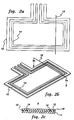
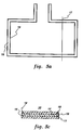
- Figure 2(a) and 2(b) illustrate a very simple drive and sense element fabricated in the same layer in both top planar and perspective views while Figure 2(c) illustrates a cross section through the simple drive and sense element which have been fabricated into a single layer structure using High Density Interconnect multilayer fabrication technology.
- these elements are distinguished by light and dark shading, although either element can operate as a drive or sense element.
- the elements shown are of differing metallized segment widths. This is simply a convenience for the sake of illustration and does not preclude segment elements of equal widths.
- element 12 is designated as a drive element and element 14 is designated as a sense element.
- element 14 is designated as a sense element.
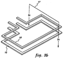
- Figures 3(a) and 3(b) 16 and 18 are designated as drive and sense elements respectively.
- Effective inductive coupling through the inspection surface requires that sense element segments be positioned in close proximity to drive element segments. The closeness of these elements to one another is seen in Figures 2(a) 2(b), 3(a) and 3(b).
- Figure 2(c) illustrates a cross sectional view through the single layer structure 9 of Figures 2(a) and 2(b) taken as indicated at 13.
- the single layer structure 9 of Figure 2(c) is comprised of a flexible substrate 11 such as KaptonTM, a polyimide available from E.I.
- a metallized pattern comprising sense element 14 and drive element 12 have been disposed either directly or after an initial deposition of an intervening dielectric layer (not shown).
- This metal pattern disposition is accomplished by first depositing a layer of metallization using sputtering or electroplating techniques to deposit titanium and copper for example, then patterning with a suitable photo resist to radiation expose a pattern of drive and sense elements from the metallized layer. Thereafter, an etching step erodes away all metal but the patterned elements 12, 14.
- These metallization, patterning and etching steps are accomplished using a photo-lithographic fabrication technique that is capable of achieving precision and uniformity at small dimensions.
- High Density Interconnect (HDI) technology accomodates such a technique of fabrication.
- HDI fabrication technology is described in detail in co-pending application serial no. (RD-20,155) entitled " A Flexible Interconnected System” by Charles W. Eichelberger, et al.
- the width of sense element segments 14 and drive element segments 12 may be the same or different.
- a layer of dielectric 19, like siloxane polyimide, is applied thereupon by spin coating.
- Figure 3(c) illustrates a crossectional view taken at 17 through the double layer structure 10 of Figures 3(a) and 3(b).
- a similar fabrication procedure is followed; however the metallization and dielectric application steps are repeated resulting in the multi-layer structure 10 shown.
- FIGS. 2(c) and 3(c) illustrate several interlayer and intralayer configurational options available when flexible multiple layer probe array elements are fabricated using High Density Interconnect fabrication technology. HDI fabrication accomodates a flexible substrate using photo-lithographic means to achieve a level of intricacy and precision heretofore unattainable by conventional means.
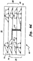
- Figure 4 illustrates some typical elements of a simple eddy current probe array having a single drive element disposed in a back and forth, serpentine arrangement providing long parallel segments disposed in an underlying layer with four associated sense elements disposed in at least another overlying layer.
- Drive element 21 is lightly shaded in the figure to indicate that it resides in a first layer of a multi-layer structure.
- Direction of current flow in the drive element is indicated by arrows.
- the four darker shaded sense elements are herein shown to have narrower metallization widths than those of the underlying drive elements.
- Various configurations for sense elements in a single layer structure include: a single loop in absolute configuration 23, a double-loop in absolute configuration 24, a single turn, double loop in differential configuration 25 and a double turn, double loop in differential configuration 22.
- Sense element 23 is a single turn, single layer, sense element in absolute configuration disposed in close proximity to the underlying drive element 21.
- Sense element 24 is a double turn, single layer sense element also in absolute configuration disposed so that the turn segments of the sense element are proximately positioned near the underlying parallel segments of the drive element 21.
- a sense element can be characterized by multiple turns connected in various configurations.
- Sense element 25 illustrates two, single turn, single layer coil elements connected in differential configuration wherein the short segment 26 between the darkened squares 27 and 28 is disposed in a layer other than that layer in which the turns of the coil element reside.
- this connection provides a "virtual ground" which operates as a common reference potential given idential induced coil voltages. This eliminates the need for a physical ground connection; thereby inherently improving eddy current probe element design.
- Interlayer metallization connections at 27 and 28 divert conduction path 26 to another layer to avoid electrically shorting the element. Both turns however, reside in the same layer.
- a similar coil element comprised of two double turn, single layer coil windings connected in differential mode is illustrated at 22 wherein the double turns of each loop reside in the same layer.
- FIG. 5 is a top planar view of four, double layer, multi-turn, conventional probe array coils, one of which is indicated by numeral 37.
- the coils are shown in an unstaggered configuration which may not be suitable for use as a probe array but illustrative of the appearance of conventional sense and drive coil elements.
- Coils 32 and 34 are wound in the same direction while remaining coils 36 and 38 are wound in the opposite direction.
- a representative connection line 31 electrically connects coil element 32 to respective contact pad 33.
- Each of the other coil elements 34, 36 and 38 are connected in a similar manner to their respective contact pads. Coils are electrically connected to one another as well as to external current sources and output leads using these contact pads.
- Probe test element 30 is comprised of two layers, each layer containing four, coplanar coils.
- the top planar view of Figure 5 shows only the coils of the top layer 32, 34, 36 and 38.
- Four similar coils (not shown) are disposed in a layer beneath the one shown in Figure 5.
- a representative connection line 35 is identified using a dotted line to illustrate electrical communication to similarly situated underlying coils (not shown) disposed in an underlying layer.
- Such coils are designated as sense and drive coils by providing appropriate electrical connection thereto.
- Designated sense and drive coils are proximately disposed with respect to one another in order to provide sufficient inductive coupling through the surface under inspection.
- Designated sense coils responsively cooperate with designated drive coils when said drive coils are electrically driven by an external alternating current source (not shown).
- a drive source is connected across a designated drive coil at respective contact pads.
- an output lead is connected across a designated sense coil at its respective contact pads.
- Figure 6(a) and 6(b) illustrate a top planar and perspective view of a coil element 45 comprised of two. three-turn coil windings 50, 60 disposed in separate but adjacent layers and centrally connected in a serial manner as a probe element.
- the lighter shaded, wider coil segments of underlying coil winding 50 are disposed as shown in Figure 6(c) in a first layer 19 beneath a second layer 20 in which coil 60 is disposed.
- Coil 60 is indicated by darker shaded, narrower coil segments.
- the darkened square 68 indicates an interlayer electrical connection between respective coil layers 19 and 20. Such a connection is accomodated by laser drilling or chemically forming a precision hole through dielectric layer 19 before a second metallization layer is applied thereon.
- Arrows 59 and 69 indicate the direction of current flow through coil element 45 at an instant in time.
- the crossectional view of Figure 6(c) is taken as indicated at numeral 40 in Figures 6(a) and 6(b).
- the instanteous current flow in each crossectionally viewed coil segment of Figure 6(c) is identified using engineering conventions, "+”, indicating current flow into the plane of the page and, ".”, indicating current flow out of the plane of the page .
- numerals identifying coil segments have been preserved in Figures 6(a)-6(c) to facilitate crossectional visualization of the multilayer fabrication of coil element 45 using a High Density Interconnect (HDI) process.
- HDI High Density Interconnect
- the process involves first patterning coil 50 onto a flexible substrate 11 such as KaptonTM, a polyimide available from E.I. DuPont de Nemours Company, which has been bonded to a support carrier (not shown).
- the support carrier is typically made of KovarTM steel, to support flexible substrate 11 throughout (HDI) processing in order to avoid shrinking, wrinkling, etc.
- substrate 11 could be a ferrite material.
- Substrate 11 is adhesively laminated to the support carrier by pretreating with a thermoplastic adhesive such as ULTEMTM polyetherimide (not shown) available from the General Electric Company which upon heating will form a reversible bond; thus, permitting easy removal of the flexible substrate 11 from the support carrier after HDI processing but otherwise remaining stable during the fabrication process.
- the flexible Kapton substrate 11 is usually, 12.5 -25 microns thick.
- a metal etched photo-lithographic procedure is used to apply a metallized pattern.
- Application of a metallization layer proceeds by sputtering a metal such as Titanium and Copper followed by electroplating or simply electroplating. Patterning includes forming the first layer of planar three turn coils corresponding to segments 51, 52, 53, 54, 55, 56, and 57 shown in crossection in Figure 6(c) with instanteous current flow indicated.
- the metallization can be applied directly to the flexible substrate; or an intervening layer of dielectric (not shown) can be deposited onto which coil 50 is then patterned. Patterning is usually accomplished using a laser exposed photo-lithographic resist process on the metallization which is followed by etching with an etchant like ferric chloride. After patterning of coil 50, a dielectric layer 19, like siloxane polyimide, is spin coat deposited thereon. Each layer of metallized coils patterned directly onto the Kapton substrate 11 (or indirectly onto an intervening dielectric (not shown)) is covered by spin coating thereon a subsequent layer of dielectric, like siloxane polyimide.
- additional Kapton can be laminated to the structure using siloxane polyimide/epoxy adhesive (not shown).
- Thicknesses of the metallization layers are approximately .2 mils. Widths of metallized coils range from 1 - 2 mils. Coil winding separation distances range from 1 - 4 mils. Dielectric layer spacing between interlayer coil windings range from .5 to 1.2 mils. If need be, large portions of the dielectric can be removed by laser ablation. Typical electrical connection "via" holes are laser drilled into the applied dielectric layer to align top surface connection sites with appropriate underlying contact pads. Connecting vias provide interlayer electrical connections fabricated by metallization to be substantially normal to the coplanar layers.
- central via 68 between double layer coil windings 50 and 60.
- Typical vias are about 1 square mil in size and downwardly tapered at a slant of about 60 degrees to accommodate uniform metallization coverage.
- a short plasma etch is used to remove debris and residual film from drilled via holes.
- Laser drilling ensures reliable, precise control of via profiles which are critical to effective electrical connection and coil design.
- Chemical means also exist to produce suitable vias.
- a second metallization layer is similarly deposited using sputtering or electroplating to a depth of about 2 - 20 microns onto dielectric layer 19 extending into via hole 68 and providing electrical connection to contact pad 54 disposed thereunder.
- Intricate metallization patterns like the rectangular windings 61, 62, 63, 64, 65, 66 and 67 of coil 60 are provided by depositing a continuous layer of metal using sputtering or electroplating; then, patterning coil windings using radiation exposed photoresist and etching with a suitable etchant in a photo-lithographic step of the HDI process. Etched metallization strip widths of approximately .0015 inch with .0035 inch pitch are achievable. Thereupon another insulating layer of dielectric 20 is applied. Current flows in the same direction in coils 50 and 60. The application of a dielectric layer, followed by drilling, metallization, patterning and etching are steps that can be repeated to provide complex, multi-layer structures.
- connection pads like 54 is computer controlled, wherein such control is based on positional information, to promote a design layout responsive to thermal dissipation, impedance control, etc.
- HDI fabrication accomodates a computerized capability for making adaptive interconnections to provide a probe pattern design which compensates for variability in operating characteristics.
- These adaptive control features provide highly reliable fabrication of precise, high density interconnect eddy current probe arrays quickly, consistently and in bulk. Design dictates where connections can be made although for convenience electrical contacts are usually edge oriented. Connections and mountings can be customized or standard depending on I/O requirements and requirements of the specific application. Conductive leads (not shown) to or from respective vias are patterned as part of each layer's metallization process.
- Conductive leads transmit signals from various probe element components within a layer to the edge of the HDI structure in order to connect to external current sources, and output devices.
- Application of the uppermost dielectric 20 constitutes a passivation layer. Laser ablation is sometimes used to carve away multi-layer deposits if necessary.
- the structure 58 may then be laminated onto a preformed ferrite substrate (not shown). This ferrite may be flexible. The presence of a ferrite backing plate (not shown) operates to intensify magnetic flux penetration into a conductive inspection surface. Depending upon the conductivity of the ferrite, it may be advantageous to interpose a layer of dielectric between the ferrite and the first layer of metal coil windings.
- the support carrier (not shown) is removed by suitable heating after HDI processing is completed.
- Figure 7 illustrates the option of offsetting coil element windings of one layer 41 with respect to those of another adjacent layer 42.
- the relative positioning of the metal coil windings with respect to one another governs capacitive coupling between the windings; the strength of which depends on the width 43, 44 of the respective windings and the dielectric separation 46 between them.
- Figure 7 also illustrates not only independent choice of winding widths but also inter-winding spacings. Winding width 43, 44 and spacing 47,48 constitute the "pitch" 49, 94 of each coil.
- the choice of pitch for each coil element is a design choice.
- Figure 8(a) illustrates a top planar view of two, three-turn, double coil elements 70, 80 deposited in separate, though not adjacent, layers.
- Figure 8(b) and 8(c) illustrate a top planar and corresponding perspective view of the composite multi-layer structure of coil elements 70 and 80.
- the crossectional view of Figure 8(d) is taken at numeral 85 as indicated in Figure 8(b) and 8(c).
- Each coil element pair is comprised of two planar coil windings.
- Coil element 70 is comprised of coil windings 71 and 72 which reside in layers 19 and 74 respectively wherein layer 20 is interposed therebetween.
- Coil element 80 is comprised of coil windings 81 and 82 residing in layers 75 and 20 respectively wherein layer 74 is interposed therebetween.
- Each coil element 70, 80 is fabricated to form multi-layer structure 76 in a manner similar to that of Figure 6(c), but having an intervening layer interposed therebetween; wherein the lower coil winding 82 of the upper coil element 80 is disposed in the intervening layer of the lower coil element 70, and the upper coil winding 71 of the lower coil element 70 is disposed in the intervening layer of the upper coil element 80.
- the central "via" connection 77 of coil 70 is illustrated in Figures 8(b) and 8(c). Current flow is shown by arrows in Figures 8(a) 8(b) and 8(c) and indicated using engineering conventions "+” and ".” in those coil segments shown in cross section in Figure 8(d).
- Either coil could be utilized as a drive or sense coil, depending on which is driven by an external current source (not shown). In fact, both coils could operate as two drive coils, if both are externally driven (not shown); or two sense coils, if both are inductively coupled to an externally driven drive coil.
- the drive coil may be deposited in the layer furthest from the inspection surface having wider coil width than the underlying sense coil. Delineating drive and sense coils in a particular configuration can establish one surface of the probe array as the probe sensitive surface.
- coil element 80 comprising coil windings 81 and 82 is used for driving while coil element 70 comprising coils windings 71 and 72 is used for sensing surface 83 is established as the probe sensitive surface.
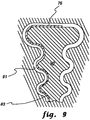
- Figure 9 illustrates the use of ferrite or some other core material to fashion a scanning form 90 onto which a two dimensional flexible HDI fabricated eddy current probe array 76 can be suitably surface bonded.
- the probe sensitive surface 83 of the array is exposed in a conforming fashion to the conductive surface 91 under inspection. Conformability is provided by surface conforming form 90, wherein affixed, probe sensitive surface 83 forms an oppositely signed, close fitting complement to the irregular surface under inspection 91.
- the entire surface or just part of the surface of the surface conforming scanning form 90 may be occupied by the two dimensional, flexible eddy current probe array 76. Affixing the eddy current probe array to scanning form 90 expedites inspection of difficult geometries which cannot be inspected by conventional scanning means.
- inspection surface 91 exhibits translational symmetry along an axis of translation, herein taken to be normal to the plane of Figure 8, inspection can be accomplished in a single axial translation of form 90 along the inspection surface 91. This presumes the probe sensing elements are sufficiently distributed to provide complete coverage in a single scan.
- drive and sense coils are not configured in obvious "coil” configurations are within the scope of this invention.
- Sufficient, uniform drive coverage can be accomplished by configuring the drive coil in long parallel, serpentine drive line segments causing current flow to be alternately oppositely directed in adjacent parallel drive line segments. It is recommended that sense lines be positioned near drive lines to promote coupling; and as already mentioned, staggering of sense coil elements must be sufficient to provide complete scan coverage and eliminate sensitivity nulls.
- Drive coil design is based on presenting a uniform drive, while sense coil design is typically tailored to the requirements of the inspection application and the specific geometry of the surface under inspection.
- Sense coils of varying shapes turns and sizes being electrically interconnected in various ways can be disposed in overlapping layers to provide a capability for selectively varying eddy current probe array sensitivity. In this way flux penetration is selectively varied into the inspection surface by selectively driving various coils of the same probe array. This provides an array with an inherent selective sensitivity feature.
- eddy current probe array When a flexible, HDI fabricated, eddy current probe array is used in conjunction with a multi-channel, multi-frequency eddy current inspection system for industrial nondestructive near surface flaw detection, measurement collection speed and accuracy are improved; thus, increasing inspection productivitly. Furthermore, when utilized in conjunction with such a system, flaw detection and characterization are improved through the implementation of parallel signal processing in image processing. These improvements are made possible by simultaneously collecting a plurality of spatially correlated measurements using an eddy current measurement array enabling formatting of the plurality of measurements for parallel image processing.
Landscapes
- Chemical & Material Sciences (AREA)
- Chemical Kinetics & Catalysis (AREA)
- Electrochemistry (AREA)
- Physics & Mathematics (AREA)
- Health & Medical Sciences (AREA)
- Life Sciences & Earth Sciences (AREA)
- Analytical Chemistry (AREA)
- Biochemistry (AREA)
- General Health & Medical Sciences (AREA)
- General Physics & Mathematics (AREA)
- Immunology (AREA)
- Pathology (AREA)
- Investigating Or Analyzing Materials By The Use Of Magnetic Means (AREA)
Applications Claiming Priority (2)
| Application Number | Priority Date | Filing Date | Title |
|---|---|---|---|
| US696455 | 1991-05-06 | ||
| US07/696,455 US5389876A (en) | 1991-05-06 | 1991-05-06 | Flexible eddy current surface measurement array for detecting near surface flaws in a conductive part |
Publications (3)
| Publication Number | Publication Date |
|---|---|
| EP0512796A2 true EP0512796A2 (fr) | 1992-11-11 |
| EP0512796A3 EP0512796A3 (en) | 1993-05-19 |
| EP0512796B1 EP0512796B1 (fr) | 1997-08-06 |
Family
ID=24797138
Family Applications (1)
| Application Number | Title | Priority Date | Filing Date |
|---|---|---|---|
| EP92304047A Expired - Lifetime EP0512796B1 (fr) | 1991-05-06 | 1992-05-05 | Réseaux de sondes à courant de foucault |
Country Status (4)
| Country | Link |
|---|---|
| US (1) | US5389876A (fr) |
| EP (1) | EP0512796B1 (fr) |
| JP (1) | JPH05142205A (fr) |
| DE (1) | DE69221367T2 (fr) |
Cited By (21)
| Publication number | Priority date | Publication date | Assignee | Title |
|---|---|---|---|---|
| EP0829713A1 (fr) * | 1996-09-13 | 1998-03-18 | Intercontrole | Sonde à courants de Foucault, pour le contrÔle non destructif de pièces électriquement conductrices |
| EP0887642A1 (fr) * | 1997-06-23 | 1998-12-30 | General Electric Company | Sonde combinant un transducteur ultrasonique flexible avec un capteur de courants de Foucault flexible |
| WO1999023484A1 (fr) * | 1997-11-04 | 1999-05-14 | Siemens Aktiengesellschaft | Palpeur pour essai par courants de foucault, procede de production d'un palpeur pour essai par courants de foucault, et procede d'essai par courants de foucault |
| DE19757575C1 (de) * | 1997-12-23 | 1999-07-15 | Siemens Ag | Elektromagnetische Untersuchungseinrichtung, geeignet für Materialuntersuchung, mit Wirbelstrommeßkopf sowie Verfahren zum Betrieb derselben |
| EP1111379A1 (fr) * | 1999-12-22 | 2001-06-27 | General Electric Company | Sonde à courants de Foucault avec un capteur en forme de lame monté sur l'extrémité flexible de la sonde, et son usage |
| WO2004083845A1 (fr) * | 2003-03-14 | 2004-09-30 | The Boeing Company | Sonde a courant de foucault bidimensionnelle et procede d'inspection associe |
| GB2401947A (en) * | 2003-04-18 | 2004-11-24 | Jentek Sensors Inc | High throughput absolute flaw imaging |
| EP1033571A3 (fr) * | 1999-03-04 | 2004-12-22 | intelligeNDT Systems & Services GmbH & Co. KG | Capteur de courant de Foucault et méthode pour sa production |
| US6911826B2 (en) | 2001-06-12 | 2005-06-28 | General Electric Company | Pulsed eddy current sensor probes and inspection methods |
| EP1600769A1 (fr) * | 2004-05-27 | 2005-11-30 | General Electric Company | Sonde omnidirectionnelle à courants de Foucault |
| US7389206B2 (en) | 2006-08-10 | 2008-06-17 | General Electric Company | Inspection systems and methods of operation |
| EP2056103A1 (fr) * | 2007-11-05 | 2009-05-06 | General Electric Company | Sonde de réseau à courant de Foucault flexible et son procédé d'assemblage |
| EP2056102A2 (fr) | 2007-11-05 | 2009-05-06 | General Electric Company | Sonde de courant de Foucault et son procédé d'assemblage |
| EP2192602A1 (fr) * | 2008-11-29 | 2010-06-02 | General Electric Company | Systèmes composites, articles incorporant le système, procédés pour test in situ, non destructif de ceux-ci et sondes de réseau utiles pour les procédés |
| WO2012072725A1 (fr) | 2010-12-02 | 2012-06-07 | Universiteit Gent | Filtres fibreux |
| EP2623976A3 (fr) * | 2012-02-06 | 2014-06-18 | General Electric Company | Inspection de disque de turbine à gaz utilisant une sonde à courant de Foucault flexible |
| US9759686B2 (en) | 2011-05-13 | 2017-09-12 | General Electric Company | Magnetic inspection systems for inspection of target objects |
| EP3336535A1 (fr) * | 2016-12-14 | 2018-06-20 | Rolls-Royce plc | Sonde à courant de foucault flexible et procédé d'utilisation correspondant |
| GB2557719A (en) * | 2016-10-17 | 2018-06-27 | Boeing Co | Three-dimensional gap measurement systems and methods |
| US10352684B2 (en) | 2016-10-17 | 2019-07-16 | The Boeing Company | Three-dimensional gap measurement systems and methods |
| EP4332565A1 (fr) * | 2022-09-05 | 2024-03-06 | General Electric Company | Ensemble capteur flexible |
Families Citing this family (84)
| Publication number | Priority date | Publication date | Assignee | Title |
|---|---|---|---|---|
| US5453689A (en) * | 1991-12-06 | 1995-09-26 | Massachusetts Institute Of Technology | Magnetometer having periodic winding structure and material property estimator |
| US5463201A (en) * | 1993-02-04 | 1995-10-31 | Generla Electric Company | Seam-tracking apparatus for a welding system employing an array of eddy current elements |
| US5659248A (en) * | 1994-10-17 | 1997-08-19 | General Electric Company | Multilayer eddy current probe array for complete coverage of an inspection surface without mechanical scanning |
| US6420867B1 (en) | 1997-03-13 | 2002-07-16 | Jentek Sensors, Inc. | Method of detecting widespread fatigue and cracks in a metal structure |
| US5793206A (en) * | 1995-08-25 | 1998-08-11 | Jentek Sensors, Inc. | Meandering winding test circuit |
| US5801532A (en) * | 1996-07-30 | 1998-09-01 | General Electric Company | Hand-holdable eddy-current probe |
| US5841277A (en) * | 1996-07-30 | 1998-11-24 | General Electric Company | Hand-holdable probe having a flexible eddy current sensor |
| US6781387B2 (en) | 1997-01-06 | 2004-08-24 | Jentek Sensors, Inc. | Inspection method using penetrant and dielectrometer |
| WO1998030921A2 (fr) * | 1997-01-06 | 1998-07-16 | Jentek Sensors, Inc. | Detection d'objets subsurfaces par magnetometre et dielectrometre |
| US6486673B1 (en) | 1997-01-06 | 2002-11-26 | Jentek Sensors, Inc. | Segmented field dielectrometer |
| US6534974B1 (en) | 1997-02-21 | 2003-03-18 | Pemstar, Inc, | Magnetic head tester with write coil and read coil |
| WO1998037429A1 (fr) * | 1997-02-21 | 1998-08-27 | Pemstar, Inc. | Appareil d'essai de tete magnetique d'enregistrement |
| US5903147A (en) * | 1997-03-18 | 1999-05-11 | General Electric Company | Eddy current array inspection device for shaped holes |
| DE19731790A1 (de) * | 1997-07-24 | 1999-01-28 | Bosch Gmbh Robert | Einrichtung zum Erfassen eines Wechselstromes |
| US5895871A (en) * | 1997-07-25 | 1999-04-20 | General Electric Company | Finger controlled inspection apparatus |
| CA2308166C (fr) * | 1997-10-29 | 2007-09-04 | Jentek Sensors, Inc. | Mesurage des proprietes absolues avec capacite d'etalonnage dans l'air ambiant |
| AU1405199A (en) | 1997-11-14 | 1999-06-07 | Jentek Sensors, Inc. | Multiple frequency quantitative coating characterization |
| US6114849A (en) * | 1998-04-17 | 2000-09-05 | United Western Technologies Corp. | Flexible eddy current test probe |
| WO1999058989A1 (fr) * | 1998-05-12 | 1999-11-18 | Jentek Sensors, Incorporated | Procede d'utilisation de signaux dielecytrometriques utilisant des grilles d'estimation |
| US6252393B1 (en) | 1998-06-23 | 2001-06-26 | General Electric Company | System and method for normalizing and calibrating a sensor array |
| DE69942172D1 (de) * | 1998-08-06 | 2010-05-06 | Mitsubishi Heavy Ind Ltd | Wirbelstromsonde zur detektion von fehlern |
| US7290476B1 (en) | 1998-10-20 | 2007-11-06 | Control Products, Inc. | Precision sensor for a hydraulic cylinder |
| US6707540B1 (en) | 1999-12-23 | 2004-03-16 | Kla-Tencor Corporation | In-situ metalization monitoring using eddy current and optical measurements |
| US6433541B1 (en) | 1999-12-23 | 2002-08-13 | Kla-Tencor Corporation | In-situ metalization monitoring using eddy current measurements during the process for removing the film |
| DE50011024D1 (de) * | 2000-06-16 | 2005-09-29 | Amo Automatisierung Mestechnik | Induktives Längenmesssystem |
| US6727691B2 (en) | 2000-06-26 | 2004-04-27 | Jentek Sensors, Inc. | High resolution inductive sensor arrays for material and defect characterization of welds |
| US6545467B1 (en) * | 2000-10-27 | 2003-04-08 | General Electric Company | Contoured surface eddy current inspection system |
| US7385392B2 (en) * | 2000-11-13 | 2008-06-10 | Jentek Sensors, Inc. | Eddy current sensing arrays and system |
| AR033080A1 (es) * | 2001-04-02 | 2003-12-03 | Sentec Ltd | Sensor de corriente |
| US6720775B2 (en) * | 2001-06-12 | 2004-04-13 | General Electric Company | Pulsed eddy current two-dimensional sensor array inspection probe and system |
| WO2003030298A1 (fr) * | 2001-08-23 | 2003-04-10 | Broadcom Corporation | Dispositif de formation d'interfaces magnetiques et applications afferentes |
| US6670808B2 (en) | 2001-08-27 | 2003-12-30 | General Electric Company | Self reference eddy current probe, measurement system, and measurement method |
| US6545469B1 (en) | 2001-10-31 | 2003-04-08 | General Electric Company | Embedded eddy current inspection apparatus, system, and method |
| EP1329730A1 (fr) | 2002-01-17 | 2003-07-23 | Siemens Aktiengesellschaft | Sonde de mesure sur substrat flexible |
| US7100861B2 (en) * | 2002-01-23 | 2006-09-05 | Control Products, Inc. | Lead guide for cable extension type position sensors |
| US7093361B2 (en) * | 2002-01-23 | 2006-08-22 | Control Products, Inc. | Method of assembling an actuator with an internal sensor |
| US6741074B2 (en) | 2002-03-01 | 2004-05-25 | General Electric Company | Method and apparatus for separating electrical runout from mechanical runout |
| US7411390B2 (en) * | 2002-06-04 | 2008-08-12 | Jentek Sensors, Inc. | High resolution inductive sensor arrays for UXO |
| US20040257072A1 (en) * | 2003-06-19 | 2004-12-23 | Rock Samson | Dual-sensitivity eddy current test probe |
| EP1496355A1 (fr) | 2003-07-09 | 2005-01-12 | Siemens Aktiengesellschaft | Sonde de mesure électrique, en particulier pour mesurer des courants de Foucault |
| US6888347B2 (en) * | 2003-09-12 | 2005-05-03 | General Electric Company | Omnidirectional eddy current probes, array probes, and inspection systems |
| US7197974B2 (en) * | 2004-01-15 | 2007-04-03 | Control Products Inc. | Position sensor |
| US7026811B2 (en) * | 2004-03-19 | 2006-04-11 | General Electric Company | Methods and apparatus for eddy current inspection of metallic posts |
| US7609055B2 (en) * | 2004-07-21 | 2009-10-27 | Control Products, Inc. | Position sensing device and method |
| US20060132123A1 (en) * | 2004-12-22 | 2006-06-22 | General Electric Company | Eddy current array probes with enhanced drive fields |
| US7626383B1 (en) | 2005-04-25 | 2009-12-01 | Innovative Materials Testing Technologies, Inc. | Apparatus and method for holding a rotatable eddy-current magnetic probe, and for rotating the probe around a boundary |
| JP4608666B2 (ja) * | 2005-05-27 | 2011-01-12 | 双日マシナリー株式会社 | 鉄系構造物の劣化診断装置 |
| US7560920B1 (en) | 2005-10-28 | 2009-07-14 | Innovative Materials Testing Technologies, Inc. | Apparatus and method for eddy-current scanning of a surface to detect cracks and other defects |
| EP1952135A4 (fr) * | 2005-11-03 | 2011-12-14 | Coastal Res Corp | Réseau à courant de foucault convivial |
| US7994780B2 (en) * | 2007-09-14 | 2011-08-09 | General Electric Company | System and method for inspection of parts with an eddy current probe |
| US8013600B1 (en) | 2007-11-19 | 2011-09-06 | Sandia Corporation | Mountable eddy current sensor for in-situ remote detection of surface and sub-surface fatigue cracks |
| GB2468097B (en) * | 2007-12-28 | 2012-06-13 | Gen Electric | Process and apparatus for testing a component using an omni-directional eddy current probe |
| CA2711168A1 (fr) * | 2007-12-31 | 2009-07-09 | General Electric Company | Procede de compensation des reponses de sondes a courant de foucault |
| DE102008027525B4 (de) * | 2008-06-03 | 2015-02-26 | Fraunhofer-Gesellschaft zur Förderung der angewandten Forschung e.V. | Wirbelstromsonde |
| US7956607B2 (en) * | 2008-09-09 | 2011-06-07 | General Electric Company | Digital ferromagnetic part inspection |
| US8269489B2 (en) * | 2008-11-25 | 2012-09-18 | General Electric Company | System and method for eddy current inspection of parts with complex geometries |
| US8812254B2 (en) * | 2009-02-18 | 2014-08-19 | General Electric Company | Methods and systems for monitoring stator winding vibration |
| CN101576534B (zh) * | 2009-03-10 | 2011-12-14 | 林俊明 | 一种以手指触觉为辅助手段的涡流检测方法及装置 |
| GB0918221D0 (en) * | 2009-10-16 | 2009-12-02 | Cambridge Silicon Radio Ltd | Inductor structure |
| US8344478B2 (en) * | 2009-10-23 | 2013-01-01 | Maxim Integrated Products, Inc. | Inductors having inductor axis parallel to substrate surface |
| US9190738B2 (en) * | 2010-04-11 | 2015-11-17 | Broadcom Corporation | Projected artificial magnetic mirror |
| US8896300B2 (en) | 2010-07-08 | 2014-11-25 | Olympus Ndt Inc. | 2D coil and a method of obtaining EC response of 3D coils using the 2D coil configuration |
| US8704513B2 (en) * | 2011-02-16 | 2014-04-22 | Olympus Ndt Inc. | Shielded eddy current coils and methods for forming same on printed circuit boards |
| JP2012242358A (ja) * | 2011-05-24 | 2012-12-10 | Kobe Steel Ltd | 渦流探傷装置 |
| FR2979790B1 (fr) * | 2011-09-07 | 2013-10-11 | Commissariat Energie Atomique | Capteur de courant |
| US8884614B2 (en) | 2011-10-31 | 2014-11-11 | General Electric Company | Eddy current array probe |
| US10241080B2 (en) * | 2011-11-07 | 2019-03-26 | Nissan Motor Co., Ltd. | Magnet evaluation device and method |
| JP2014074638A (ja) * | 2012-10-04 | 2014-04-24 | Kyocera Document Solutions Inc | 差動トランス式磁気センサー |
| JP5544406B2 (ja) * | 2012-10-12 | 2014-07-09 | 東京理学検査株式会社 | 渦流探傷装置 |
| JP5820795B2 (ja) * | 2012-10-15 | 2015-11-24 | 京セラドキュメントソリューションズ株式会社 | 画像形成装置 |
| EP2746795B1 (fr) * | 2012-12-20 | 2015-10-07 | Alstom Technology Ltd | Dispositif et procédé pour mesurer le champ magnétique dans l'entrefer d'une machine électrique |
| DE102013216019A1 (de) | 2013-08-13 | 2015-02-19 | Magnetische Prüfanlagen Gmbh | Mehrschicht-Wirbelstromsonde, Verfahren zur Herstellung einer Mehrschicht-Wirbelstromsonde und Prüfgerät mit Mehrschicht-Wirbelstromsonde |
| US9322806B2 (en) * | 2013-10-25 | 2016-04-26 | General Electric Company | Eddy current sensor with linear drive conductor |
| DE102013222523A1 (de) * | 2013-11-06 | 2015-05-07 | Magnetische Prüfanlagen Gmbh | Wirbelstromsonde und Wirbelstrom-Prüfgerät |
| US20160290781A1 (en) * | 2013-11-08 | 2016-10-06 | Empire Technology Development Llc | Apparatus and methods for detecting substrate alignment during a printing process |
| US9408298B2 (en) * | 2014-03-18 | 2016-08-02 | Eaton Corporation | Flexible circuit Rogowski coil |
| US10209223B2 (en) | 2015-05-26 | 2019-02-19 | The Boeing Company | Real-time fusion of ultrasound and eddy current data during non-destructive examination |
| DE102017107708A1 (de) | 2017-04-10 | 2018-10-11 | Prüftechnik Dieter Busch AG | Differenzsonde, Prüfvorrichtung und Herstellungsverfahren |
| CN109541018A (zh) * | 2018-11-19 | 2019-03-29 | 厦门大学 | 一种柔性周向交叉阵列涡流传感薄膜及其监测裂纹的方法 |
| KR102802030B1 (ko) | 2020-04-22 | 2025-05-02 | 삼성메디슨 주식회사 | 초음파 프로브 |
| JP2023141887A (ja) * | 2022-03-24 | 2023-10-05 | 原子燃料工業株式会社 | 多層フレキシブルプリント基板、渦電流探傷検査コイル、渦電流探傷検査装置および渦電流探傷検査方法 |
| CN118251648A (zh) * | 2022-07-22 | 2024-06-25 | 深圳市韶音科技有限公司 | 一种可穿戴设备 |
| JP7647711B2 (ja) * | 2022-08-30 | 2025-03-18 | 横河電機株式会社 | 磁気パイプセンサ |
| CN121311769A (zh) * | 2023-06-14 | 2026-01-09 | 加拿大埃维登特有限公司 | 用于无损检测的挠性探头衬垫 |
Family Cites Families (12)
| Publication number | Priority date | Publication date | Assignee | Title |
|---|---|---|---|---|
| US3271662A (en) * | 1962-08-22 | 1966-09-06 | Api Instr Company | Flaw detecting apparatus having multiple pick-up and exciting coils on the same side of the test piece |
| SE301731B (fr) * | 1966-02-24 | 1968-06-17 | Essem Metotest Ab | |
| SU700830A1 (ru) * | 1978-06-08 | 1979-11-30 | Кубанский Ордена Трудового Красного Знамени Сельскохозяйственный Институт | Токовихревой накладной преобразователь |
| JPS55113947A (en) * | 1979-02-26 | 1980-09-02 | Electron Kiyooto:Kk | Flaw detector for cast iron pipe |
| CA1194117A (fr) * | 1981-10-09 | 1985-09-24 | Richard T. Dewalle | Detecteurs de courants de foucault et methode de fabrication |
| US4706021A (en) * | 1983-08-08 | 1987-11-10 | The Charles Stark Draper Laboratory, Inc. | Crossed wire defect detector employing eddy currents |
| US4593245A (en) * | 1983-12-12 | 1986-06-03 | General Electric Company | Eddy current method for detecting a flaw in semi-conductive material |
| EP0228177A3 (fr) * | 1985-11-19 | 1988-11-02 | Electric Power Research Institute, Inc | Bobine flexible de courant tourbillonnaire et disposition de bobines d'essais non destructif |
| SE456863B (sv) * | 1986-07-15 | 1988-11-07 | Toernbloms Kvalitetskontroll | Maet- och/eller kontrollanordning utnyttjande virvelstroemsteknik med undertryckning av godartade ytdeformationer |
| CH673896A5 (en) * | 1988-01-28 | 1990-04-12 | Asea Brown Boveri | Non-destructive eddy-current tester - has pairs of coils excited and sampled by multiplexer in clock circuit pre-programmed for computerised scanning of flexible test mat |
| CH677152A5 (fr) * | 1989-02-08 | 1991-04-15 | Asea Brown Boveri | |
| US5047719A (en) * | 1990-05-25 | 1991-09-10 | The Failure Group, Inc. | Flexible coil assembly for reflectance-mode nondestructive eddy-current examination |
-
1991
- 1991-05-06 US US07/696,455 patent/US5389876A/en not_active Expired - Lifetime
-
1992
- 1992-04-30 JP JP4111359A patent/JPH05142205A/ja active Pending
- 1992-05-05 EP EP92304047A patent/EP0512796B1/fr not_active Expired - Lifetime
- 1992-05-05 DE DE69221367T patent/DE69221367T2/de not_active Expired - Fee Related
Cited By (29)
| Publication number | Priority date | Publication date | Assignee | Title |
|---|---|---|---|---|
| FR2753534A1 (fr) * | 1996-09-13 | 1998-03-20 | Intercontrole Sa | Sonde a courants de foucault, pour le controle non destructif de pieces electriquement conductrices |
| EP0829713A1 (fr) * | 1996-09-13 | 1998-03-18 | Intercontrole | Sonde à courants de Foucault, pour le contrÔle non destructif de pièces électriquement conductrices |
| EP0887642A1 (fr) * | 1997-06-23 | 1998-12-30 | General Electric Company | Sonde combinant un transducteur ultrasonique flexible avec un capteur de courants de Foucault flexible |
| WO1999023484A1 (fr) * | 1997-11-04 | 1999-05-14 | Siemens Aktiengesellschaft | Palpeur pour essai par courants de foucault, procede de production d'un palpeur pour essai par courants de foucault, et procede d'essai par courants de foucault |
| DE19757575C1 (de) * | 1997-12-23 | 1999-07-15 | Siemens Ag | Elektromagnetische Untersuchungseinrichtung, geeignet für Materialuntersuchung, mit Wirbelstrommeßkopf sowie Verfahren zum Betrieb derselben |
| EP1033571A3 (fr) * | 1999-03-04 | 2004-12-22 | intelligeNDT Systems & Services GmbH & Co. KG | Capteur de courant de Foucault et méthode pour sa production |
| EP1111379A1 (fr) * | 1999-12-22 | 2001-06-27 | General Electric Company | Sonde à courants de Foucault avec un capteur en forme de lame monté sur l'extrémité flexible de la sonde, et son usage |
| US6911826B2 (en) | 2001-06-12 | 2005-06-28 | General Electric Company | Pulsed eddy current sensor probes and inspection methods |
| WO2004083845A1 (fr) * | 2003-03-14 | 2004-09-30 | The Boeing Company | Sonde a courant de foucault bidimensionnelle et procede d'inspection associe |
| US6914427B2 (en) | 2003-03-14 | 2005-07-05 | The Boeing Company | Eddy current probe having sensing elements defined by first and second elongated coils and an associated inspection method |
| GB2401947A (en) * | 2003-04-18 | 2004-11-24 | Jentek Sensors Inc | High throughput absolute flaw imaging |
| EP1600769A1 (fr) * | 2004-05-27 | 2005-11-30 | General Electric Company | Sonde omnidirectionnelle à courants de Foucault |
| US7015690B2 (en) | 2004-05-27 | 2006-03-21 | General Electric Company | Omnidirectional eddy current probe and inspection system |
| US7389206B2 (en) | 2006-08-10 | 2008-06-17 | General Electric Company | Inspection systems and methods of operation |
| EP2056103A1 (fr) * | 2007-11-05 | 2009-05-06 | General Electric Company | Sonde de réseau à courant de Foucault flexible et son procédé d'assemblage |
| EP2056102A3 (fr) * | 2007-11-05 | 2009-11-25 | General Electric Company | Sonde de courant de Foucault et son procédé d'assemblage |
| US7888932B2 (en) | 2007-11-05 | 2011-02-15 | General Electric Company | Surface flaw detection system to facilitate nondestructive inspection of a component and methods of assembling the same |
| EP2056102A2 (fr) | 2007-11-05 | 2009-05-06 | General Electric Company | Sonde de courant de Foucault et son procédé d'assemblage |
| EP2192602A1 (fr) * | 2008-11-29 | 2010-06-02 | General Electric Company | Systèmes composites, articles incorporant le système, procédés pour test in situ, non destructif de ceux-ci et sondes de réseau utiles pour les procédés |
| US8378668B2 (en) | 2008-11-29 | 2013-02-19 | General Electric Company | Method for non-destructive testing of composite systems |
| WO2012072725A1 (fr) | 2010-12-02 | 2012-06-07 | Universiteit Gent | Filtres fibreux |
| US9759686B2 (en) | 2011-05-13 | 2017-09-12 | General Electric Company | Magnetic inspection systems for inspection of target objects |
| EP2623976A3 (fr) * | 2012-02-06 | 2014-06-18 | General Electric Company | Inspection de disque de turbine à gaz utilisant une sonde à courant de Foucault flexible |
| GB2557719A (en) * | 2016-10-17 | 2018-06-27 | Boeing Co | Three-dimensional gap measurement systems and methods |
| US10240909B2 (en) | 2016-10-17 | 2019-03-26 | The Boeing Company | Three-dimensional gap measurement systems and methods |
| US10352684B2 (en) | 2016-10-17 | 2019-07-16 | The Boeing Company | Three-dimensional gap measurement systems and methods |
| GB2557719B (en) * | 2016-10-17 | 2021-02-03 | Boeing Co | Three-dimensional gap measurement systems and methods |
| EP3336535A1 (fr) * | 2016-12-14 | 2018-06-20 | Rolls-Royce plc | Sonde à courant de foucault flexible et procédé d'utilisation correspondant |
| EP4332565A1 (fr) * | 2022-09-05 | 2024-03-06 | General Electric Company | Ensemble capteur flexible |
Also Published As
| Publication number | Publication date |
|---|---|
| US5389876A (en) | 1995-02-14 |
| JPH05142205A (ja) | 1993-06-08 |
| EP0512796A3 (en) | 1993-05-19 |
| EP0512796B1 (fr) | 1997-08-06 |
| DE69221367D1 (de) | 1997-09-11 |
| DE69221367T2 (de) | 1998-03-19 |
Similar Documents
| Publication | Publication Date | Title |
|---|---|---|
| EP0512796B1 (fr) | Réseaux de sondes à courant de foucault | |
| US5510709A (en) | Eddy current surface inspection probe for aircraft fastener inspection, and inspection method | |
| US5262722A (en) | Apparatus for near surface nondestructive eddy current scanning of a conductive part using a multi-layer eddy current probe array | |
| US5659248A (en) | Multilayer eddy current probe array for complete coverage of an inspection surface without mechanical scanning | |
| US20050007108A1 (en) | Probes and methods for detecting defects in metallic structures | |
| US5182513A (en) | Method and apparatus for a multi-channel multi-frequency data acquisition system for nondestructive eddy current inspection testing | |
| US3504276A (en) | Printed circuit coils for use in magnetic flux leakage flow detection | |
| JP4662539B2 (ja) | 多方向距離無接触測定器 | |
| US5382898A (en) | High density probe card for testing electrical circuits | |
| US5047719A (en) | Flexible coil assembly for reflectance-mode nondestructive eddy-current examination | |
| US4855677A (en) | Multiple coil eddy current probe and method of flaw detection | |
| KR101697812B1 (ko) | 와전류 센서 및 연마 방법 및 장치 | |
| US7098655B2 (en) | Eddy-current sensor with planar meander exciting coil and spin valve magnetoresistive element for nondestructive testing | |
| JP7781594B2 (ja) | 走査素子とこの走査素子を備えた誘導式位置測定装置 | |
| US6975108B2 (en) | Methods and devices for eddy current PCB inspection | |
| JPH1151905A (ja) | 渦流探傷装置用探傷コイルアレイおよび該探傷コイルアレイを用いた渦流探傷方法 | |
| US20050270041A1 (en) | Non-contact capacitive sensor and cable with dual layer active shield | |
| WO1994008248A1 (fr) | Procede et systeme de mise a l'essai sans contact de plaquettes de circuits imprimes | |
| JPH08278342A (ja) | 導体回路基板の検査方法およびその検査装置 | |
| US9322806B2 (en) | Eddy current sensor with linear drive conductor | |
| EP0228177A2 (fr) | Bobine flexible de courant tourbillonnaire et disposition de bobines d'essais non destructif | |
| JP3376731B2 (ja) | 高周波用のプリント基板及びこれを用いたプローブカード | |
| JP5215303B2 (ja) | 分離した放射/受信機能により導電部の渦電流検査を行う方法及びデバイス | |
| GB2273782A (en) | Eddy current flaw detection of sheet metal adjacent fasteners | |
| EP0369393A2 (fr) | Positionnement d'un ouvrage de préssion par un moyen de mesure électrique |
Legal Events
| Date | Code | Title | Description |
|---|---|---|---|
| PUAI | Public reference made under article 153(3) epc to a published international application that has entered the european phase |
Free format text: ORIGINAL CODE: 0009012 |
|
| AK | Designated contracting states |
Kind code of ref document: A2 Designated state(s): DE FR GB IT |
|
| PUAL | Search report despatched |
Free format text: ORIGINAL CODE: 0009013 |
|
| AK | Designated contracting states |
Kind code of ref document: A3 Designated state(s): DE FR GB IT |
|
| 17P | Request for examination filed |
Effective date: 19931102 |
|
| 17Q | First examination report despatched |
Effective date: 19951103 |
|
| GRAG | Despatch of communication of intention to grant |
Free format text: ORIGINAL CODE: EPIDOS AGRA |
|
| GRAH | Despatch of communication of intention to grant a patent |
Free format text: ORIGINAL CODE: EPIDOS IGRA |
|
| GRAH | Despatch of communication of intention to grant a patent |
Free format text: ORIGINAL CODE: EPIDOS IGRA |
|
| GRAA | (expected) grant |
Free format text: ORIGINAL CODE: 0009210 |
|
| AK | Designated contracting states |
Kind code of ref document: B1 Designated state(s): DE FR GB IT |
|
| ET | Fr: translation filed | ||
| REF | Corresponds to: |
Ref document number: 69221367 Country of ref document: DE Date of ref document: 19970911 |
|
| ITF | It: translation for a ep patent filed | ||
| PLBE | No opposition filed within time limit |
Free format text: ORIGINAL CODE: 0009261 |
|
| STAA | Information on the status of an ep patent application or granted ep patent |
Free format text: STATUS: NO OPPOSITION FILED WITHIN TIME LIMIT |
|
| 26N | No opposition filed | ||
| REG | Reference to a national code |
Ref country code: GB Ref legal event code: IF02 |
|
| PGFP | Annual fee paid to national office [announced via postgrant information from national office to epo] |
Ref country code: DE Payment date: 20070702 Year of fee payment: 16 |
|
| PGFP | Annual fee paid to national office [announced via postgrant information from national office to epo] |
Ref country code: GB Payment date: 20070525 Year of fee payment: 16 |
|
| PGFP | Annual fee paid to national office [announced via postgrant information from national office to epo] |
Ref country code: IT Payment date: 20070526 Year of fee payment: 16 |
|
| PGFP | Annual fee paid to national office [announced via postgrant information from national office to epo] |
Ref country code: FR Payment date: 20070517 Year of fee payment: 16 |
|
| GBPC | Gb: european patent ceased through non-payment of renewal fee |
Effective date: 20080505 |
|
| REG | Reference to a national code |
Ref country code: FR Ref legal event code: ST Effective date: 20090119 |
|
| PG25 | Lapsed in a contracting state [announced via postgrant information from national office to epo] |
Ref country code: DE Free format text: LAPSE BECAUSE OF NON-PAYMENT OF DUE FEES Effective date: 20081202 Ref country code: FR Free format text: LAPSE BECAUSE OF NON-PAYMENT OF DUE FEES Effective date: 20080602 |
|
| PG25 | Lapsed in a contracting state [announced via postgrant information from national office to epo] |
Ref country code: GB Free format text: LAPSE BECAUSE OF NON-PAYMENT OF DUE FEES Effective date: 20080505 |
|
| PG25 | Lapsed in a contracting state [announced via postgrant information from national office to epo] |
Ref country code: IT Free format text: LAPSE BECAUSE OF NON-PAYMENT OF DUE FEES Effective date: 20080505 |