EP0514005A2 - Abtast- und Halteschaltung - Google Patents
Abtast- und Halteschaltung Download PDFInfo
- Publication number
- EP0514005A2 EP0514005A2 EP92303326A EP92303326A EP0514005A2 EP 0514005 A2 EP0514005 A2 EP 0514005A2 EP 92303326 A EP92303326 A EP 92303326A EP 92303326 A EP92303326 A EP 92303326A EP 0514005 A2 EP0514005 A2 EP 0514005A2
- Authority
- EP
- European Patent Office
- Prior art keywords
- capacitors
- input
- voltages
- sample
- operational amplifier
- Prior art date
- Legal status (The legal status is an assumption and is not a legal conclusion. Google has not performed a legal analysis and makes no representation as to the accuracy of the status listed.)
- Granted
Links
- 239000003990 capacitor Substances 0.000 claims abstract description 57
- 238000005070 sampling Methods 0.000 claims abstract description 5
- 238000010586 diagram Methods 0.000 description 3
- 239000004973 liquid crystal related substance Substances 0.000 description 2
- 239000011159 matrix material Substances 0.000 description 2
- 230000003247 decreasing effect Effects 0.000 description 1
Images


Classifications
-
- G—PHYSICS
- G11—INFORMATION STORAGE
- G11C—STATIC STORES
- G11C27/00—Electric analogue stores, e.g. for storing instantaneous values
- G11C27/02—Sample-and-hold arrangements
- G11C27/024—Sample-and-hold arrangements using a capacitive memory element
- G11C27/026—Sample-and-hold arrangements using a capacitive memory element associated with an amplifier
Definitions
- the present invention relates to a sample-and-hold circuit.
- Analog signals are input to the sample-and-hold circuit through signal lines V1 to Vn.
- the sample-and-hold circuit is provided with capacitors C1 to Cn and capacitors D1 to Dn for sampling and holding input voltages from the signal lines (the capacities of those capacitors include wire capacitances and stray capacitances). Ends on one side of the capacitors C1 to Cn are connected to the signal lines V1 to Vn through the analog switches S1 to Sn which are turned on and off by control signals SS1 to SSn, respectively, and the other ends of the capacitors C1 to Cn are all connected to ground.
- Ends on one side of the capacitors D1 to Dn are connected to the ends on one side of the capacitors C1 to Cn through analog switches H1 to Hn which are turned on and off by a control signal HS.
- the other ends of the capacitors D1 to Dn are connected to ground.
- Noninverting input terminals of operational amplifier circuits P1 to Pn are connected to the ends on one side of the capacitors D1 to Dn, respectively, while the inverting input terminals are connected to output terminals thereof, respectively.
- the output terminals of the operational amplifier circuits P1 to Pn are tied to a common line.
- Output control signals CN1 to CNn are input respectively to the operational amplifiers.
- the object of the present invention can be achieved by a sample-and-hold circuit comprising a plurality of first capacitors, respectively connected to a plurality of input signal lines through respective first analog switches, for sampling input signal voltages, a plurality of second capacitors, respectively connected to the plurality of first capacitors through respective second analog switches, for holding the sampled voltages, and a single operational amplifier for selectively receiving one of the voltages held in the plurality of second capacitors according to a control signal supplied thereto, and amplifying and outputting the received voltage.
- a plurality of input signals to be sampled are taken into a plurality of first capacitors, and then, held respectively in a plurality of second capacitors.
- the operational amplifier selects one of the voltages held in the plurality of the second capacitors, and amplifies and outputs it according to contents of a control signal supplied from the outside. Therefore, it is not necessary to provide a plurality of an operational amplifier according to each capacitor.
- the operational amplifier may include a first input connected to an output thereof, a plurality of second inputs connected to ends of the second capacitors, respectively, a control signal input for a control signal supplied from the outside, and mechanism for selecting one of the second inputs as a noninverting input according to the control signal.
- control signal input includes a plurality of binary signal inputs.
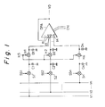
- Fig. 1 shows a sample-and-hold circuit according to the present invention, which constitutes a part of an active matrix type liquid crystal driver circuit.
- Analog signals are input to this sample-and-hold circuit through signal lines V1 to Vn.
- the sample-and-hold circuit is provided with capacitors C1 to Cn and capacitors D1 to Dn for sampling and holding signal voltages from the signal lines (the capacities of the capacitors include wire capacitances and stray capacitances). Ends on one side of the capacitors C1 to Cn are connected to the signal lines V1 to Vn through analog switches S1 to Sn which are turned on and off by control signals SS1 to SSn.
- the other ends of the capacitors C1 to Cn are all connected to ground. Ends on one side of the capacitors D1 to Dn are connected to the ends on one side of the capacitors C1 to Cn through analog switches H1 to Hn which are turned on and off by a control signal HS. The other ends of the capacitors D1 to Dn are connected to ground.
- an operational amplifier circuit OPA having input terminals I1 to In for receiving the voltages held in the capacitors D1 to Dn.
- the operational amplifier circuit OPA selects one of the voltages supplied to the input terminals I1 to by means of a selection signal CNi, and uses the selected voltage as a noninverting input voltage.
- the inverting input terminal of the operational amplifier circuit OPA is connected to the output terminal thereof.
- the operational amplifier circuit OPA selects one of the voltages supplied to the input terminals I1 to In according to the contents of the signal, and uses this selected voltage as the noninverting input. Therefore, for example, in case that a selection signal CNi is applied which specifies that the voltage of the input terminal I1 be selected, the operational amplifier circuit OPA gets the voltage held in the capacitor D1 as a noninverting voltage, and sends it out as the output Vo. By varying the contents of the control signal CNi, the operational amplifier circuit OPA is made to sequentially output the voltages held in the capacitors D1 to Dn as the output Vo.
- the operational amplifier OPA is basically a differential amplifier and has the arrangement shown in Fig. 2.
- the operational amplifier OPA according to the example in Fig. 2 is provided with two noninverting terminals I1 and I2. Therefore, the voltages held in the capacitors connected to the noninverting terminals, respectively, are output sequentially as the output Vo from the amplifier.
- One terminal of an n-channel MOS transistor N57 is connected to the ground, and a potential Vb is applied to the gate of the transistor N57.
- Each one terminal of p-channel MOS transistors P51, P52 is connected to a power supply VDD and each gate of the transistors P51, P52 is connected to the other terminal of the transistor P51.
- Each one terminal of n-channel MOS transistors N56, N53 is connected to the other terminal of the transistor N57.
- the other terminals of the transistors N56, N53 are connected to the other terminal of the transistor P51 through the MOS transistors N55, N51, respectively.
- the gates of the transistors N56, N53 are connected to the non-inverting input terminals I1 and I2 of the operational amplifier OPA, respectively.
- Control signals CNi are applied to the gates of the transistors N55 and N51 respectively.
- An n-channel MOS transistor N54 whose gate is connected to the inverting input terminal is connected between the other terminal of the transistor P52 through the n-channel MOS transistor N52 and the other terminal of the transistor N57.
- a contact of the transistors N52 and P52 is connected to the output terminal Vo of the operational amplifier OPA.
- the gate of the transistor N52 is connected to the power supply VDD.
- the operational amplifier circuit selectively receives one of the voltages held in a plurality of capacitors according to the contents of the control circuit supplied from outside, and amplifies and outputs the received voltage. Therefore, it is not necessary to provide a plurality of an operational amplifier circuit according to each capacitor. As a result, the number of devices constituting the circuit can be decreased and the chip area required for forming the circuit as an integrated circuit can be reduced.
Landscapes
- Liquid Crystal Display Device Control (AREA)
- Electronic Switches (AREA)
- Analogue/Digital Conversion (AREA)
- Amplifiers (AREA)
Applications Claiming Priority (2)
| Application Number | Priority Date | Filing Date | Title |
|---|---|---|---|
| JP82396/91 | 1991-04-15 | ||
| JP3082396A JP2698225B2 (ja) | 1991-04-15 | 1991-04-15 | サンプルホールド回路 |
Publications (3)
| Publication Number | Publication Date |
|---|---|
| EP0514005A2 true EP0514005A2 (de) | 1992-11-19 |
| EP0514005A3 EP0514005A3 (en) | 1993-01-13 |
| EP0514005B1 EP0514005B1 (de) | 1997-06-18 |
Family
ID=13773431
Family Applications (1)
| Application Number | Title | Priority Date | Filing Date |
|---|---|---|---|
| EP92303326A Expired - Lifetime EP0514005B1 (de) | 1991-04-15 | 1992-04-14 | Abtast- und Halteschaltung |
Country Status (4)
| Country | Link |
|---|---|
| US (1) | US5304866A (de) |
| EP (1) | EP0514005B1 (de) |
| JP (1) | JP2698225B2 (de) |
| DE (1) | DE69220416T2 (de) |
Families Citing this family (9)
| Publication number | Priority date | Publication date | Assignee | Title |
|---|---|---|---|---|
| US5481212A (en) * | 1993-03-12 | 1996-01-02 | Kabushiki Kaisha Toshiba | Sample-and-hold circuit device |
| JP3222276B2 (ja) * | 1993-07-30 | 2001-10-22 | セイコーインスツルメンツ株式会社 | コンパレータ回路およびコンパレータ回路の制御方法 |
| JPH0845298A (ja) * | 1994-07-29 | 1996-02-16 | Nec Corp | 差動サンプル・ホールド回路 |
| JP3208299B2 (ja) * | 1995-02-20 | 2001-09-10 | シャープ株式会社 | アクティブマトリクス方式液晶駆動回路 |
| WO2000025174A1 (fr) * | 1998-10-28 | 2000-05-04 | Hitachi, Ltd. | Circuit d'alimentation commandant des cristaux liquides et affichage a cristaux liquides correspondant |
| JP2002300542A (ja) * | 2001-04-03 | 2002-10-11 | Mitsubishi Electric Corp | データスライサ回路 |
| JP2002368592A (ja) * | 2001-06-11 | 2002-12-20 | Oki Electric Ind Co Ltd | サンプル・ホールド回路 |
| TWI300936B (en) * | 2006-07-03 | 2008-09-11 | Novatek Microelectronics Corp | A high-accuracy sample and hold circuit |
| JP4900065B2 (ja) * | 2006-10-19 | 2012-03-21 | 株式会社デンソー | マルチチャネルサンプルホールド回路およびマルチチャネルa/d変換器 |
Family Cites Families (10)
| Publication number | Priority date | Publication date | Assignee | Title |
|---|---|---|---|---|
| JPS5085265A (de) * | 1973-11-28 | 1975-07-09 | ||
| DE2718175C2 (de) * | 1977-04-23 | 1983-12-15 | Licentia Patent-Verwaltungs-Gmbh, 6000 Frankfurt | Abtast-Halte-Schaltung für einen Phasendiskriminator |
| JPS57204611A (en) * | 1981-06-10 | 1982-12-15 | Toshiba Corp | Voltage follower circuit |
| JPS619900A (ja) * | 1984-06-25 | 1986-01-17 | Nippon Gakki Seizo Kk | サンプル・ホ−ルド回路 |
| JPS6242399A (ja) * | 1985-08-19 | 1987-02-24 | Nec Corp | サンプルホ−ルド回路 |
| DE3616818A1 (de) * | 1986-05-17 | 1987-11-19 | Philips Patentverwaltung | Schaltung zum umsetzen von drei-zustands-signalen in binaere signale |
| JPH02134006A (ja) * | 1988-11-14 | 1990-05-23 | Nec Corp | 増幅回路 |
| JP2520162B2 (ja) * | 1988-12-07 | 1996-07-31 | キヤノン株式会社 | 相関2重サンプリング回路 |
| JPH0389545A (ja) * | 1989-08-31 | 1991-04-15 | Sharp Corp | 集積回路のためのキャパシタ |
| US5162670A (en) * | 1990-01-26 | 1992-11-10 | Kabushiki Kaisha Toshiba | Sample-and-hold circuit device |
-
1991
- 1991-04-15 JP JP3082396A patent/JP2698225B2/ja not_active Expired - Fee Related
-
1992
- 1992-04-14 DE DE69220416T patent/DE69220416T2/de not_active Expired - Fee Related
- 1992-04-14 US US07/868,213 patent/US5304866A/en not_active Expired - Lifetime
- 1992-04-14 EP EP92303326A patent/EP0514005B1/de not_active Expired - Lifetime
Also Published As
| Publication number | Publication date |
|---|---|
| EP0514005B1 (de) | 1997-06-18 |
| EP0514005A3 (en) | 1993-01-13 |
| DE69220416T2 (de) | 1998-01-02 |
| JPH04315897A (ja) | 1992-11-06 |
| DE69220416D1 (de) | 1997-07-24 |
| JP2698225B2 (ja) | 1998-01-19 |
| US5304866A (en) | 1994-04-19 |
Similar Documents
| Publication | Publication Date | Title |
|---|---|---|
| KR100564275B1 (ko) | 액정표시장치 | |
| US6529049B2 (en) | Pre-charged sample and hold | |
| US5459483A (en) | Electronic device with feedback loop | |
| KR960030403A (ko) | 반도체 장치, 이 장치를 갖는 반도체 회로, 상관 연산 장치, 신호 변환기, 및 신호 처리 시스템 | |
| KR19990024003A (ko) | 액정표시장치 | |
| US5304866A (en) | Sample-and-hold circuit | |
| US3696305A (en) | High speed high accuracy sample and hold circuit | |
| JPH033515A (ja) | 積分器回路 | |
| US3638039A (en) | Operation of field-effect transistor circuits having substantial distributed capacitance | |
| US6043812A (en) | Liquid crystal drive circuit and liquid crystal display device | |
| US10868502B2 (en) | Switched capacitor circuit to make amount of change in reference voltage even regardless of input level | |
| KR870002585A (ko) | 반도체 메모리 장치 | |
| GB2072980A (en) | Dynamic shift register circuit | |
| NL8802973A (nl) | Geintegreerde geheugenschakeling. | |
| US5296751A (en) | Sample-and-hold circuit | |
| EP0810730B1 (de) | Analoge FIFO-Speicher | |
| US6091619A (en) | Array architecture for long record length fast-in slow-out (FISO) analog memory | |
| US4044342A (en) | Dynamic type semiconductor memory device | |
| US6657909B2 (en) | Memory sense amplifier | |
| US6181610B1 (en) | Semiconductor device having current auxiliary circuit for output circuit | |
| US5204838A (en) | High speed readout circuit | |
| KR950001128B1 (ko) | 반도체기억장치 | |
| Bienstman et al. | An 8 channel 8b µ P compatible NMOS converter with programmable ranges | |
| JP2994000B2 (ja) | サンプル・ホールド増幅回路 | |
| EP0696804A2 (de) | Abtast- und Halterschaltung |
Legal Events
| Date | Code | Title | Description |
|---|---|---|---|
| PUAI | Public reference made under article 153(3) epc to a published international application that has entered the european phase |
Free format text: ORIGINAL CODE: 0009012 |
|
| AK | Designated contracting states |
Kind code of ref document: A2 Designated state(s): DE FR NL |
|
| PUAL | Search report despatched |
Free format text: ORIGINAL CODE: 0009013 |
|
| AK | Designated contracting states |
Kind code of ref document: A3 Designated state(s): DE FR NL |
|
| 17P | Request for examination filed |
Effective date: 19930330 |
|
| 17Q | First examination report despatched |
Effective date: 19960214 |
|
| GRAG | Despatch of communication of intention to grant |
Free format text: ORIGINAL CODE: EPIDOS AGRA |
|
| GRAH | Despatch of communication of intention to grant a patent |
Free format text: ORIGINAL CODE: EPIDOS IGRA |
|
| GRAH | Despatch of communication of intention to grant a patent |
Free format text: ORIGINAL CODE: EPIDOS IGRA |
|
| GRAA | (expected) grant |
Free format text: ORIGINAL CODE: 0009210 |
|
| AK | Designated contracting states |
Kind code of ref document: B1 Designated state(s): DE FR NL |
|
| REF | Corresponds to: |
Ref document number: 69220416 Country of ref document: DE Date of ref document: 19970724 |
|
| ET | Fr: translation filed | ||
| PLBE | No opposition filed within time limit |
Free format text: ORIGINAL CODE: 0009261 |
|
| STAA | Information on the status of an ep patent application or granted ep patent |
Free format text: STATUS: NO OPPOSITION FILED WITHIN TIME LIMIT |
|
| 26N | No opposition filed | ||
| PGFP | Annual fee paid to national office [announced via postgrant information from national office to epo] |
Ref country code: DE Payment date: 20060406 Year of fee payment: 15 |
|
| PGFP | Annual fee paid to national office [announced via postgrant information from national office to epo] |
Ref country code: FR Payment date: 20060410 Year of fee payment: 15 |
|
| PGFP | Annual fee paid to national office [announced via postgrant information from national office to epo] |
Ref country code: NL Payment date: 20060417 Year of fee payment: 15 |
|
| NLV4 | Nl: lapsed or anulled due to non-payment of the annual fee |
Effective date: 20071101 |
|
| PG25 | Lapsed in a contracting state [announced via postgrant information from national office to epo] |
Ref country code: NL Free format text: LAPSE BECAUSE OF NON-PAYMENT OF DUE FEES Effective date: 20071101 Ref country code: DE Free format text: LAPSE BECAUSE OF NON-PAYMENT OF DUE FEES Effective date: 20071101 |
|
| PG25 | Lapsed in a contracting state [announced via postgrant information from national office to epo] |
Ref country code: FR Free format text: LAPSE BECAUSE OF NON-PAYMENT OF DUE FEES Effective date: 20070430 |