EP0514083A2 - Anzeigesystem - Google Patents
Anzeigesystem Download PDFInfo
- Publication number
- EP0514083A2 EP0514083A2 EP92304125A EP92304125A EP0514083A2 EP 0514083 A2 EP0514083 A2 EP 0514083A2 EP 92304125 A EP92304125 A EP 92304125A EP 92304125 A EP92304125 A EP 92304125A EP 0514083 A2 EP0514083 A2 EP 0514083A2
- Authority
- EP
- European Patent Office
- Prior art keywords
- light
- information
- emitting devices
- modulator
- spatial
- Prior art date
- Legal status (The legal status is an assumption and is not a legal conclusion. Google has not performed a legal analysis and makes no representation as to the accuracy of the status listed.)
- Withdrawn
Links
Images

Classifications
-
- G—PHYSICS
- G09—EDUCATION; CRYPTOGRAPHY; DISPLAY; ADVERTISING; SEALS
- G09G—ARRANGEMENTS OR CIRCUITS FOR CONTROL OF INDICATING DEVICES USING STATIC MEANS TO PRESENT VARIABLE INFORMATION
- G09G3/00—Control arrangements or circuits, of interest only in connection with visual indicators other than cathode-ray tubes
- G09G3/001—Control arrangements or circuits, of interest only in connection with visual indicators other than cathode-ray tubes using specific devices not provided for in groups G09G3/02 - G09G3/36, e.g. using an intermediate record carrier such as a film slide; Projection systems; Display of non-alphanumerical information, solely or in combination with alphanumerical information, e.g. digital display on projected diapositive as background
- G09G3/002—Control arrangements or circuits, of interest only in connection with visual indicators other than cathode-ray tubes using specific devices not provided for in groups G09G3/02 - G09G3/36, e.g. using an intermediate record carrier such as a film slide; Projection systems; Display of non-alphanumerical information, solely or in combination with alphanumerical information, e.g. digital display on projected diapositive as background to project the image of a two-dimensional display, such as an array of light emitting or modulating elements or a CRT
-
- G—PHYSICS
- G09—EDUCATION; CRYPTOGRAPHY; DISPLAY; ADVERTISING; SEALS
- G09G—ARRANGEMENTS OR CIRCUITS FOR CONTROL OF INDICATING DEVICES USING STATIC MEANS TO PRESENT VARIABLE INFORMATION
- G09G3/00—Control arrangements or circuits, of interest only in connection with visual indicators other than cathode-ray tubes
- G09G3/02—Control arrangements or circuits, of interest only in connection with visual indicators other than cathode-ray tubes by tracing or scanning a light beam on a screen
Definitions
- the present invention relates to a display system and, more particularly, to a display system including a spatial light modulator (SLM).
- SLM spatial light modulator
- a display system has been known in which a light beam whose intensity is modulated with a signal of information, is projected onto a screen by a optical projector system to display a two-dimensional image of the information.
- a conventional system utilizes an optical beam whose intensity is modulated according to pixel data of the image carried by an image signal, and the optical beam scans a display screen vertically and horizontally.
- a light source projects light rays of a rectilinear cross section onto a linear light modulator, in which the incident light rays are intensity-modulated correspondingly with pixels of information aligned in the linear light modulator, in turn, the intensity modulated light rays leave the light modulator as a light beam of a rectilinear cross section.
- the outgoing beam is deflected horizontally at a given frequency by a rotating polygon mirror and projected onto a screen via a projector lens to create a two-dimensional image.
- This improved system makes it easy to display a high-definition image with high brightness.
- the system proposed by the present Applicant as described above has a disadvantage that the intensity modulation of light in the light modulator according to the pixels of information, is slow in response.
- the present Applicant has proposed another display system as described in Japanese patent application No. 130498/1990 corresponding to U.S. patent application Ser. No. 702,817. Specifically, a stream of information to be displayed as a two dimensional image, is divided into plural pieces. A linear array of light-emitting devices is arranged to have N light-emitting devices corresponding to N pixels contained in each divided piece of the stream of information.
- the N light-emitting devices are driven with each divided piece of information as such that signals of N pixels in each divided piece of the information are concurrently supplied to their respective N light-emitting devices to light up them simultaneously and according to each divided piece of information.
- Light rays emitted from the array of light-emitting devices are concurrently deflected in a direction perpendicular to the direction of the array of the light rays. These deflected light rays impinges as writing light onto a spatial light modulator comprising at least a photoconductive layer and a light modulation layer interposed between electrodes.
- the writing light is focused onto the photoconductive layer.
- Reading light is arranged to impinge the spatial light modulator to project the image information read from the modulator onto a screen.
- the contrast ratio deteriorates.
- an intense reading light in the visible region must be directed to the spatial light modulator. In this case, the amount of the reading light leaking into the photoconductive layer of the modulator increases. As a result, it is inevitable that the contrast of the displayed image reduces.
- the present invention offers a display system for displaying information comprising a linear array of N light-emitting devices emitting light of predetermined wavelength, the devices are arranged respectively with N pixels, a stream of the information is divided into pieces each of which containing the N pixels, and the N light-emitting devices are caused to emit N light beams simultaneously in a form of array during a given period for every divided piece of the information, the every divided piece of information may correspond to one line of a frame of picture, the N light beams are intensity-modulated respectively with the divided piece of the information, the N light beams are deflected simultaneously in a direction perpendicular to a direction of the array of the N light beams, and a spatial light modulator having a photoconductive layer and a light modulation layer interposed between a pair of electrodes, the photoconductive layer is responsive to the deflected N light beams incident thereto through a focusing lens as a writing light, and comprising a reading light of visible wavelength which is shorter than the predetermined wavelength of the emitted
- the photomodulation layer may be comprised of homeotropically oriented liquid crystal having an electric field-controlled birefringence.
- a display system includes a linear array REA having N light-emitting devices in line corresponding to N pixels fed to drive thereof.
- N is a natural number equal to or greater than 2.
- the linear array REA may be comprised of light-emitting diodes, semiconductor lasers, or the like on a substrate.
- the linear array REA may be. an array of light-emitting devices with microlenses thereon.
- the linear array REA of the light-emitting devices emits writing light to a spatial light modulator SLM having a photoconductive layer PCL (described later).
- SLM spatial light modulator
- PCL photoconductive layer
- the wavelength of the writing light is so selected that it falls into a proximity of the peak of the spectral sensitivity of the photoconductive layer PCL.
- the intensity of the writing light of N light rays is distributed along the linear array of the N light emitting devices correspondingly with N pixels which constitute one line of the image to be displayed.
- the N light-emitting devices of the N light rays are driven to lit up simultaneously for a given period which may be equivalent to one scanning line period for a frame of picture in a conventional image scanning system.
- the image information to be displayed is in a form of image signal in a time domain being supplied to the display system from an image information source
- the image signal is divided into a plurality of segments each of which contains N pixels and corresponds to each of the divided pieces of the image information, and each segment (piece of the information) is converted to simultaneously presenting signals at a rate of every piece of the information by a series-to-parallel converter such as shift register.
- the intensity-modulated N light rays emitted from the N light-emitting devices of the linear array REA are directed onto an optical deflector or scanner such as a galvano-mirror Mg or revolving polygon mirror via a lens L.
- the mirror Mg vibrates in the direction indicated by the double headed arrow at a predetermined rate.
- the light rays deflected by the vibrating mirror Mg scans across a surface of the spatial light modulator SLM from its top to bottom at a scanning speed corresponding to the predetermined rate of the mirror vibration.
- the deflected light rays are focused as writing light onto the photoconductive layer of the light modulator SLM to write the image information thereon.
- the N light-emitting devices of the linear array REA are caused to emit light rays as such that they are intensity-modulated according to the information of N pixels aligned in one straight line across the image to be displayed. Similar operations are successively performed of plurality of such straight lines forming the image to be displayed. In this way, the image to be displayed is written to the spatial light modulator SLM.
- the spatial light modulator SLM used in the display system shown in Fig. 1 can be fabricated by laminating a transparent substrate BP1, a transparent electrode Et1, a photoconductive layer PCL, a dielectric mirror DML, an orientation film ALL, a light modulation layer PML, a transparent electrode Et2, and a transparent substrate BP2 interfacing each other in this order as shown in Fig. 2.
- the spatial light modulator SLM can be either of a light reflection type or a light transmission type. In the following description, the reflection type spatial light modulator is used as the spatial light modulator SLM.
- Each of the transparent electrodes Et1 and Et2 of the modulator SLM consists of a thin transparent electro-conductive material.
- the photoconductive layer PCL exhibits photoconductivity responsive in the wavelength range of the writing light.
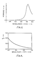
- the vertical axis of Fig. 3 represents the ratio of the impedance Zd of the photoconductive layer PCL when no light is incident on it to the impedance Zp of the photoconductive layer PCL when light is incident on it, i.e., Zd/Zp.
- the dielectric mirror DML can take a well-known form such as a multilayer film reflecting a light in the predetermined wavelength range.
- the light modulation layer PML is made of a light-modulating material which varies or modulates the mode of the light transmitted therethrough in response to the strength of the applied electric field.
- this layer PML is made of a homeotropically oriented liquid crystal exhibiting birefringence controlled by the applied electric field.
- the orientation film ALL shown in Fig. 2 is for orienting the liquid crystal homeotropically.
- a voltage supply E applies a predetermined voltage between the transparent electrodes Et1 and Et2.
- the writing light WL enters the substrate BP1 and is focused onto the photoconductive layer PCL causing the electrical resistance of the photoconductive layer PCL to reduce in response to the intensity of the writing light WL.
- This resistance reduction takes place two dimensionally over the surface of the photoconductive layer PCL as the surface is scanned with the writing light.
- a charge image is formed on the interface between the photoconductive layer PCL and the dielectric mirror DML.
- Electric potential distribution of the charge image corresponds to the amount of writing light of N light rays which scan the photoconductive layer PCL, where the N light rays are intensity modulated with the image information line by line to cove one full frame of the image to be displayed.
- the photomodulation layer PML is two dimensionally subjected to an electric field generated by the charge image.
- the wavelength of the writing light WL is selected to be in the proximity of the peak of the spectral sensitivity of the photoconductive layer PCL, which peak in this embodiment is slightly over 700 nm, which is in the near infrared region as shown in Fig.3.
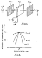
- Fig. 4 shows dependence of the index of double refraction ⁇ n of crystals or liquid crystals showing electro-optical effects on the wavelength of light.
- the index of double refraction ⁇ n varies depending on the wavelength of the light.
- the light modulation layer PML made of a nematic liquid-crystal cell, for example, is positioned between two polarizers PL1, and PL2 whose principal planes are perpendicular to each other in the crossed Nicol's relation.
- V is a driving voltage and SW indicates a switch to apply the driving voltage and SW indicates a switch to apply the driving voltage.
- the factor ⁇ ( V ) included in equation (2) is the tilt angle of the major axis of the average molecule of the liquid crystal.
- the conventional homogeneously oriented liquid crystal is driven generally with a large value of the order m, thus the intensity of the transmitted light varies greatly with its wavelength. Therefore, where a homogeneously oriented liquid crystal is employed as the light modulation layer PML, the intensity of transmitted light varies greatly with the wavelength of the reading light. Consequently, it is inevitable that the contrast ratio deteriorates. Meanwhile, the homeotropically oriented liquid crystal used in the present invention is used generally at a small value of the order m. Therefore, the intensity of the transmitted light is less affected by the wavelength value.
- the present invention using the homeotropically oriented liquid crystal presents a high contrast ratio.
- the reading light RL is produced by a light source LS.
- the reading light RL is in the visible range and does not include wavelength components to which the photoconductive layer PCL of the spatial light modulator SLM is sensitive.
- the light in the wavelength range from 420 nm to 630 nm is preferable for reading light RL for color image displays, such preferable wavelength range is utilized on the present invention unlike the writing light WL which scans the spatial light modulator SLM, the reading light RL is a signal beam of light which irradiates the modulator SLM simultaneously as follows.
- the "S" polarized component of the reading light RL is reflected toward the reading side of the spatial light modulator SLM by the beam splitter PBS and enters the transparent substrate BP2 of the moduator SLM.
- the reading light RL then passes through the transparent electrode Et2 , the light modulation layer PML comprising the homeotropically oriented liquid crystal, the orientation film ALL, and the dielectric mirror DML where the reading light RL is reflected back by the dielectric mirror DML to the orientation film ALL, passing again the light modulation layer PML, the transparent electrode Et2 , and the transparent substrate BP2.
- the reading light RL then exits out the spatial light modulator SLM.
- the reading light RL passed through twice the photomodulation layer PML undergoing the electric field produced by the effectric charge image is polarization modulated correspondingly with pixels of the image information written on the photoconductive layer PCL.
- the polarization modulated reading light RL enters the polarization beam splitter PBS.
- P polarized component of the reading light RL passes through the polarization beam splitter PBS, is projected on the screen S by the projection lens L p .
- the spatial light modulator SLM is of the reflection type.
- the inventive display system can also use a transmission type spatial light modulator.
- the N light-emitting devices of the linear array REA emit N light rays which are intensity-modulated according to the image information to be projected on displayed , and such writing light rays are focused onto the spatial light modulator SLM. These N light rays from one straight line of N light spots on the spatial light modulator at a time. And this straight line of N light spots concurrently scans the modulator SLM to write the information.
- a single beam of light is intensity-modulated with a signal carrying image information to be displayed.
- the modulated signal beam of light scans the spatial light modulator SLM sequentially by being deflected in vertical and horizontal directions to write the image information.
- the time of exposure to the writing light is N times longer in the present invention than that in the prior art. This enables the present invention system to use a low intensity light spot, thus the writing light leakage into the photoconductive layer PML is minimized.
- the photomodulation layer PML of the spatial light modulator SLM is made of a homeotropically oriented liquid crystal exhibiting electric field-controlled birefringence which is less dependent on wavelength, for example , a wide range of wavelength , e.g., from 420 nm to 630 nm in the visible region in which the photoconductive layer PCL is responsive, can be effectively utilized as the reading light RL.
- the display system of the present invention features a displayed image of bright, high resolution and high contrast ratio by utilizing a white reading light quite efficiency.
Landscapes
- Engineering & Computer Science (AREA)
- Physics & Mathematics (AREA)
- Computer Hardware Design (AREA)
- General Physics & Mathematics (AREA)
- Theoretical Computer Science (AREA)
- Liquid Crystal (AREA)
- Devices For Indicating Variable Information By Combining Individual Elements (AREA)
Applications Claiming Priority (2)
| Application Number | Priority Date | Filing Date | Title |
|---|---|---|---|
| JP3132007A JPH04333027A (ja) | 1991-05-08 | 1991-05-08 | 表示装置 |
| JP132007/91 | 1991-05-08 |
Publications (2)
| Publication Number | Publication Date |
|---|---|
| EP0514083A2 true EP0514083A2 (de) | 1992-11-19 |
| EP0514083A3 EP0514083A3 (en) | 1993-09-08 |
Family
ID=15071367
Family Applications (1)
| Application Number | Title | Priority Date | Filing Date |
|---|---|---|---|
| EP19920304125 Withdrawn EP0514083A3 (en) | 1991-05-08 | 1992-05-07 | Display system |
Country Status (3)
| Country | Link |
|---|---|
| US (1) | US5381188A (de) |
| EP (1) | EP0514083A3 (de) |
| JP (1) | JPH04333027A (de) |
Cited By (1)
| Publication number | Priority date | Publication date | Assignee | Title |
|---|---|---|---|---|
| EP0762370A3 (de) * | 1995-08-02 | 1998-01-07 | Canon Kabushiki Kaisha | Ansteuerungsverfahren für ein Anzeigegerät mit optischer Modulationsvorrichtung |
Family Cites Families (5)
| Publication number | Priority date | Publication date | Assignee | Title |
|---|---|---|---|---|
| US4150396A (en) * | 1974-09-06 | 1979-04-17 | Thomson-Csf | Erasable thermo-optic storage display of a transmitted color image |
| US3971931A (en) * | 1975-01-23 | 1976-07-27 | The United States Of America As Represented By The Secretary Of The Navy | Led image tube light valve |
| CH638623A5 (fr) * | 1980-06-11 | 1983-09-30 | Cortaillod Cables Sa | Dispositif a cristaux liquides pour visualiser le rayonnement infrarouge. |
| DE68921686T2 (de) * | 1988-08-19 | 1995-07-27 | Victor Company Of Japan | Wiedergabegerät für ein Ladungslatentbildaufzeichnungsmedium. |
| JPH0317618A (ja) * | 1989-06-15 | 1991-01-25 | Seiko Instr Inc | 光書込型液晶ライトバルブの光書込み駆動方法 |
-
1991
- 1991-05-08 JP JP3132007A patent/JPH04333027A/ja active Pending
-
1992
- 1992-05-04 US US07/878,046 patent/US5381188A/en not_active Expired - Fee Related
- 1992-05-07 EP EP19920304125 patent/EP0514083A3/en not_active Withdrawn
Cited By (2)
| Publication number | Priority date | Publication date | Assignee | Title |
|---|---|---|---|---|
| EP0762370A3 (de) * | 1995-08-02 | 1998-01-07 | Canon Kabushiki Kaisha | Ansteuerungsverfahren für ein Anzeigegerät mit optischer Modulationsvorrichtung |
| US5856814A (en) * | 1995-08-02 | 1999-01-05 | Canon Kk | Driving method for display apparatus |
Also Published As
| Publication number | Publication date |
|---|---|
| JPH04333027A (ja) | 1992-11-20 |
| US5381188A (en) | 1995-01-10 |
| EP0514083A3 (en) | 1993-09-08 |
Similar Documents
| Publication | Publication Date | Title |
|---|---|---|
| US5614962A (en) | Method for projecting image obtained by using liquid crystal panels and display apparatus for realizing the same | |
| US4611245A (en) | Real-time ultra-high resolution image projection display using laser-addressed liquid crystal light valve | |
| US5973727A (en) | Video image viewing device and method | |
| KR950014547B1 (ko) | 디스플레이 유니트 | |
| US4533215A (en) | Real-time ultra-high resolution image projection display using laser-addressed liquid crystal light valve | |
| KR960013313B1 (ko) | 전기광학 표시장치 | |
| KR0140706B1 (ko) | 다층 액정장치 | |
| JPH09511588A (ja) | 表示スクリーン | |
| US5231282A (en) | Optical writing type liquid crystal light valve and writing apparatus therefor | |
| EP0517517A1 (de) | Aus einem einzelnen Lichtventil bestehender Vollfarbenprojektor | |
| US6388697B1 (en) | Image forming device and two dimensional optical scanning device | |
| US3707323A (en) | Liquid crystal devices and systems for ultrasonic imaging | |
| JPH07199213A (ja) | 光書き込み型液晶表示記録装置 | |
| US4992880A (en) | High definition video-rate laser-addressed liquid-crystal light-valve projection display | |
| US5381188A (en) | Light to light modulator with reading light of specified wavelength | |
| JP2536694B2 (ja) | 光―光変換素子による光―光変換方法と表示装置 | |
| JPS63109422A (ja) | 画像投影機 | |
| JP3109283B2 (ja) | 液晶表示装置 | |
| US5185617A (en) | Method of information conversion and apparatus thereof | |
| JPH07104310A (ja) | 表示装置 | |
| JPH04161925A (ja) | 空間光変調素子及びその表示装置 | |
| JP3086927B2 (ja) | 小型光パターン認識装置およびその駆動方式 | |
| JPH05323123A (ja) | 光学装置 | |
| JPS6113771A (ja) | Plztを用いたラインスキヤナ− | |
| Shields et al. | Light valve and projection mode LCDs |
Legal Events
| Date | Code | Title | Description |
|---|---|---|---|
| PUAI | Public reference made under article 153(3) epc to a published international application that has entered the european phase |
Free format text: ORIGINAL CODE: 0009012 |
|
| AK | Designated contracting states |
Kind code of ref document: A2 Designated state(s): DE FR GB |
|
| PUAL | Search report despatched |
Free format text: ORIGINAL CODE: 0009013 |
|
| AK | Designated contracting states |
Kind code of ref document: A3 Designated state(s): DE FR GB |
|
| 17P | Request for examination filed |
Effective date: 19931008 |
|
| 17Q | First examination report despatched |
Effective date: 19950320 |
|
| STAA | Information on the status of an ep patent application or granted ep patent |
Free format text: STATUS: THE APPLICATION IS DEEMED TO BE WITHDRAWN |
|
| 18D | Application deemed to be withdrawn |
Effective date: 19951001 |