EP0514629A2 - Méthode de démodulation et de synchronisation des signaux modulés numériquement - Google Patents
Méthode de démodulation et de synchronisation des signaux modulés numériquement Download PDFInfo
- Publication number
- EP0514629A2 EP0514629A2 EP92103109A EP92103109A EP0514629A2 EP 0514629 A2 EP0514629 A2 EP 0514629A2 EP 92103109 A EP92103109 A EP 92103109A EP 92103109 A EP92103109 A EP 92103109A EP 0514629 A2 EP0514629 A2 EP 0514629A2
- Authority
- EP
- European Patent Office
- Prior art keywords
- symbol
- signal
- demodulation
- pattern
- memory
- Prior art date
- Legal status (The legal status is an assumption and is not a legal conclusion. Google has not performed a legal analysis and makes no representation as to the accuracy of the status listed.)
- Granted
Links
Images



Classifications
-
- H—ELECTRICITY
- H04—ELECTRIC COMMUNICATION TECHNIQUE
- H04L—TRANSMISSION OF DIGITAL INFORMATION, e.g. TELEGRAPHIC COMMUNICATION
- H04L7/00—Arrangements for synchronising receiver with transmitter
- H04L7/02—Speed or phase control by the received code signals, the signals containing no special synchronisation information
- H04L7/033—Speed or phase control by the received code signals, the signals containing no special synchronisation information using the transitions of the received signal to control the phase of the synchronising-signal-generating means, e.g. using a phase-locked loop
- H04L7/0334—Processing of samples having at least three levels, e.g. soft decisions
Definitions
- the invention relates to a method specified in the preamble of claim 1.
- the invention has for its object to reduce the computer effort in a method of the type mentioned and to provide a solution that works reliably and safely within wide limits even with disturbed transmission channel.
- the basic principle of the demodulation and synchronization method according to the invention is based on the recognition of patterns and the derived meaning of the received symbols as well as the generation of synchronization pulses which serve to track an oscillator which supplies the reference clock for the entire circuit.
- the basis of the subsequent processing is the amplitude quantization of the baseband signal obtained after hard limitation and linear FM demodulation, which is carried out at regular time intervals which are in whole-number relation to the symbol clock.
- the method according to the invention can be used particularly advantageously in connection with two- and multi-stage angle modulation methods with constant amplitude.
- the process is not coherent in the classic sense. Instead, a relatively hard limitation can be applied so that automatic gain control (AGC) is not required and remarkable insensitivity to frequency and phase errors is achieved.
- AGC automatic gain control
- the synchronization of the symbol clock f s can best be derived from the symbol edge.
- T s is the symbol duration.
- the PLL circuit contains a gate for masking out the reference pulses if no edge pulse is generated, as is the case when there is no information change, that is to say with 1-1 and 0-0 transitions. This means that only 0-1 and 1-0 transitions have an influence on the demodulation result.
- Phase jumps can be compensated for by a digital auxiliary loop, which can be implemented very easily as a counter. If the expected impulse does not fall into the expectation window several times, this auxiliary loop can be used to make a quick transition to the new position in one or more steps with an expanded expectation window.
- the definition of the window size and the correction step size is critical and, if necessary, determined experimentally. The aim is to maintain the synchronization with the lowest possible S / N ratio.
- demodulation takes place by means of pattern recognition and is characterized in more detail below.
- the signal curve piece that comes closest to one of the expected pattern curves is assumed to be received.
- the size of the deviation can be used as a quality criterion, and irregular states due to disturbances in the transmission path can also be specially identified. Both support the successful decoding of disturbed signals when using certain types of error-detecting codes.
- a preferred embodiment is based on the fact that the corresponding pattern, which is scanned with the correct symbol clock, is recorded over the symbol length T s in the case of centering towards the center of the symbol and is compared with the stored pattern curves.
- the pattern sought is then that which has, for example, the smallest sum of the square differences to the received pattern.
- this requires a large number of comparisons, especially for higher-quality modulation types or when scanning over more than one symbol duration, which also requires fast hardware at higher transmission rates.
- a further preferred embodiment makes use of the possibility that certain characteristics are extracted from the time course, from which the symbol content can be calculated.
- Such procedures are partial Computationally intensive and rely on complicated and extensive algorithms, the processing of which requires high-performance hardware at higher transmission speeds, which is usually also quite expensive.
- a preferred third method uses a memory for demodulation.
- Some digitized amplitude values of the received signal serve as addresses for a memory in which there is directly the associated result, which was originally obtained by quasi-symmetrical considerations or with a suitable algorithm, self-learning systems also being suitable.
- the memory content can be directly assigned to the pattern by means of a suitable address arrangement.
- Illegal addresses or combinations of states can be used directly to output a quality criterion.
- an address space of 216 to 220 should not be exceeded in order to be able to economically implement the required memory.
- This principle is as simple as it is powerful because it is ultimately based on a type of associative storage.
- To implement it only simple hardware is required, which mainly consists of memories whose maximum operating speed is in the MHz range, while the focus here is on digital transmission via mobile radio channels at transmission speeds of only a few hundred kbit / s based.
- the eight to sixteen times symbol clock is sometimes required as the working speed, so that certain minimum requirements must be placed on the speed of the hardware.
- the memory can then be the most likely sub-symbol sequence, e.g. B. "010", a fault message 1 or 0 and a quality criterion with (k-1) bit, here 3 bit, so that a result word contains 8 bits in this case.
- a ROM of 32 kByte is sufficient.
- bit clock pulses can also be derived. They are set to the center of the edge in the memory and appear when the middle of a 0-1 or 1-0 transition has just been reached and
- ⁇ p O / 2nd is maximum.
- the pattern memory can thus be used for demodulation and for synchronous clock acquisition at the same time.
- sampling over several symbol periods is also possible. In the case of several symbol periods, five sampling periods represent preferred values. For a sampling with data words of four bits results an address space of 220. This also allows a longer part of a symbol sequence to be decoded, such as the symbols "01" or the likely neighboring symbol sequence, for example "0010". If these are combined with a signal bit obtained on the basis of an interference criterion and three bits characterizing the signal quality, a signal sequence of 8 bits is obtained. The resulting memory requirement is 1 MB.
- the method according to the invention can be used advantageously in particular if, instead of an amplitude and mean normalization, deviations from the central position are taken into account in the decoding.
- averaging over several successive symbols can be used.
- the averaging uses the fact that several pieces of information are obtained about one symbol, for example a symbol content "1" and a probable partial sequence "010".
- the averaging can be taken over by a memory.
- the address space results from the number of linked symbols multiplied by the number of quantization bits per symbol.
- 3 x 4 bits follows, i.e. an address space of 212.
- the center of the symbol is given a higher rating. But you can also only look at the symbol and the adjacent edges and get, for example, the symbol "1" from the edge 01 and the neighboring edges 0-1 and 1-0 the word "01110", which is why the symbol under consideration has its meaning "1" can be assigned.
- Synchronization and demodulation can be realized on the basis of a simple pattern recognition by means of two memories connected in series and are therefore very easy to manufacture in an integrated form.
- the method according to the invention is particularly suitable for so-called "higher modulation types" and partial response methods.
- an appropriate extension to multi-stage modulation types such as CP-4FSK (2RC)
- CP-4FSK (2RC) is favorable.
- this requires a slightly higher-level quantization, which results in a higher memory requirement, so that the effort increases.
- scanning over two symbols becomes relatively complex since the required address space of the pattern memory becomes quite large.
- sample I-ROM contents of the sample I-ROM can be obtained by quasi-geometric considerations, as has already been indicated. Majority decisions are then taken as a basis for the sample II ROM, for example the sequence "+”, “1", “-” ("+” and “-” stand for rising or falling edges) is a clear indication of a received one "1", which will most likely be between two zeros. If a total of more than 50% probability for "1" is found with all values, the state in question is finally declared as "1" - the same applies to "0".
- sample II-ROM is to be made much larger if the averaging is to be carried out directly with the digitized signal values, the sample I-ROM must first have the quantized signal values in a likewise quantized preliminary result, not just the logical value "1 "or” 0 ", have converted and made available.
- the quality information can then be used in two ways. On the one hand, she can use the pattern II ROM to obtain the average signal quality, on the other hand it can be used when decoding the information in the sample I-ROM, provided that an error-correcting code is used that can make useful use of this information, as is possible with some code families constructed in this regard.
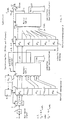
- the baseband signal appearing at an input connection 1 reaches a low-pass filter 2 and is there freed from disturbing harmonic components.
- the output of the low pass 2 is connected to the input of an analog-digital converter 3.
- This D / A converter quantizes the baseband signal with a width of 4 bits, for example.
- This digitization is preferably carried out with the eight or sixteen times symbol clock, ie each "symbol" is sampled eight times or six times in equidistant time intervals and thus converted into eight or sixteen digital words of 4 bits in length.
- This clock is generated by a clock generator 4, the output signal of which also reaches the clock input of a first word shift register 5, which receives the digital output signal of the A / D converter at its data input.
- the word shift register 5 holds nine words of 4 bits each for addressing a downstream ROM memory 6. (The waveform of the corresponding "sample I comparison" for raw demodulation and synchronization are shown schematically in FIG. 2a.)
- the clock signal of the clock generator 4 has a clock rate which is so high that the possibility of synchronization of the signal in digital processing has a sufficiently fine grid. If, for example, the sixteenth symbol clock is selected for sufficiently precise synchronization, the first word shift register 5 must be made correspondingly longer. However, since only the beginning, end and end of the symbol are required, an address space in the ROM memory 6 of 12 bits is sufficient.
- a synchronizing pulse With a ROM memory with a capacity of 32 kbytes, a synchronizing pulse, a fault message bit, three bits characterizing the signal quality and three bits for identifying the information content of the respectively decoded curve section of the relevant signal section - for example "010" - be preserved.
- a further (second) word shift register 8 is connected downstream of the output of the first ROM 6, the output lines, ie the lines on which the information content of the decoded curve segment appears, being connected to the data input of the second word shift register.
- the reading out of the first ROM 6 and the clocking of the second shift register 8 takes place with the double symbol clock, ie with the sampling clock of the clock generator 4 which is reduced by a factor of four.
- the reduced clock (for example 2 fsymb ) is provided at the input 7.
- the coupling between the clock of the clock generator 4 and the input 7 for the reduced clock is not rigid, but is dependent on the synchronization with the input signal, whereby this synchronization means a fixed phase position in relation to the symbols of the input signal, so that the further processing can be carried out symbol-synchronously.
- Synchronous pulses (mids or flanks) as output pulses of the ROM 6 reach the clock generator 4 via a phase locked loop (PLL system).
- PLL system phase locked loop
- the information contents of the symbols form a word sequence in the second word shift register 8, which is used for addressing a further ROM 9 connected downstream of the shift register 8.
- the word sequence contained in the shift register 8 corresponds to five successive curve elements and represents the decoded information content of two successive symbols. (The corresponding signal relationships are shown schematically in FIG. 2b).
- Averaging is carried out with the addressing of the ROM memory 9, the segments of the curve - in a symbolizing representation, for example, having the sequence "FMFMF". "F” stands for flank and "M” for middle.
- the averaging of the information content of two symbols of the input signal takes place in the sample ROM 9.
- the latter has - in the example shown - an address space of 215 and provides the decoded information as well as an averaged quality criterion, which means that a necessary amount of memory of 16 kByte is available results.
- the averaged decoded information appears at the output of the ROM 9.
- a clock signal f SYMB is available at an input 10 and corresponds to the rate of the symbols appearing at the input.
- the decoded information consisting of the averaged "O" and "1" values is one Output 12 supplied.
- the scope of the second memory is reduced considerably, in the present example to 0.25 kbytes.
- the clock frequency at the input 7 is thus also reduced to half, ie it then only has to be clocked with f s , the rate of arrival of the symbols at the input, and no longer with 2 ⁇ f s , and the gate 11 at the decoding output can likewise omitted.
- What is essential in the operation of the demodulation and synchronization method according to the invention is the recognition of patterns and the derived meaning of the received symbols as well as the acquisition of synchronous pulses, which are used in particular to track the oscillator 4, which provides the reference clock for the entire circuit.
- amplitude quantization of the baseband signal obtained after hard limitation and linear FM demodulation which is carried out at regular intervals which are in whole-number relation to the symbol clock.
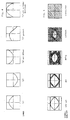
- FIG. 2a and 2b show (as already mentioned) details of the evaluation in a schematic representation.
- the assignment of the sampling times to the symbol for synchronization and raw demodulation is shown in FIG. 2a.
- the sampling times during synchronization are located at the beginning of the symbol, the middle of the symbol and at the end of the symbol.
- the signal shown in solid lines forms the symbol, while the signal edge shown in dashed lines relates to the synchronization behavior.
- FIG. 2c the conditions during the evaluation of CP-BFSK (2RC) are shown schematically:
- the symbol T to be evaluated is detected by means of the hatched evaluation window 18 within an evaluation window 18 which is limited in terms of time and amplitude and which has a raster corresponding to the course of the time to be expected in time Symbols.
- Evaluation fields 21 and 22 are provided at the beginning and end of the "window" at the zero crossing.
- evaluation fields 23 and 24 are provided in the area of the positive or negative minimum in the middle of the evaluation window.
- Further evaluation fields 25 to 28 are provided in the intermediate and temporal range.
- Figure 3 shows schematically the pattern assignment to the addresses.
- an address space of 216 to 22 Speicher appears to be suitable or should not be exceeded in order to be able to economically implement the required memory.
- This principle is so powerful because it is ultimately based on a type of associative storage. To implement it, all that is required is simple hardware, which mainly consists of memories whose maximum operating speed is in the MHz range, while the focus here on digital transmission via mobile radio channels is based on transmission speeds of only a few hundred kbit / s. However, the eight to sixteen times symbol clock is sometimes required as the working speed, so that certain minimum requirements must be placed on the speed of the hardware.
- the symbol start, the symbol center and the symbol end with k bits each, for example k 4, this results in an address space of 2 3 k , here 2 1 2.
- the memory can then have the symbol meaning, e.g. B. "010", a fault message 1 or 0 and a quality criterion with (k-1) bit, in this case 3 bit, so that a result word contains 8 bits in this case (cf. again FIG. 3).
- a ROM of 32 kByte would be sufficient. If you clock the arrangement with the eightfold symbol clock and take equidistant samples in time, you can also derive bit clock pulses.
- sampling over several symbol periods is also possible. In the case of several symbol periods, five sampling periods are preferred values.
- the address space is 220. This also allows a longer part of a symbol sequence to be decoded, such as the symbols of a "01" or the likely neighboring symbol sequence, for example "0010". If these are combined with a signal bit obtained on the basis of an interference criterion and three bits characterizing the signal quality, a signal sequence of 8 bits is obtained. The resulting memory requirement is 1 MB.
- the method according to the invention can be used advantageously in particular if, instead of an amplitude and mean normalization, deviations from the central position are taken into account in the decoding.
- FIG. 4 shows some important examples for the evaluation of disturbed symbols in the case of amplitude errors, offset errors, signal deformations and the like.
- the signal shape is automatically assigned to the meaning resulting from the overall appearance. This means that the signal shape is evaluated more precisely than with a simple threshold comparison with fixed thresholds, since the total information available is better used.
- the signal influencing by noise or interference is shown qualitatively in FIG. 5. It also becomes clear how a quality criterion can be determined from the signal position and its shape. When determining this quality criterion, preference is given to using the results when decoding several symbols. This makes it easy to obtain information about the average reception quality.
- Averaging can take advantage of the fact that more information is obtained from one symbol, e.g. Symbol "1" and probable substring "010".
- FIG. 6 shows an example of how the evaluation can be carried out.
- the averaging is fault-tolerant, so that individual incorrect information is covered, but here too, values between "1/2" and “1” or “0” and “1/2” can be used to infer the signal quality, with "1 / 2 "is intended to symbolize the middle between the amplitude values assigned to the two logic states.
- Synchronization and demodulation are realized on the basis of a simple pattern recognition by two series-connected memories and manufactured in an integrated form.
- the embodiment of the invention is not limited to the preferred exemplary embodiment specified above. Rather, a number of variants are conceivable which make use of the solution shown even in the case of fundamentally different types.
Landscapes
- Engineering & Computer Science (AREA)
- Computer Networks & Wireless Communication (AREA)
- Signal Processing (AREA)
- Digital Transmission Methods That Use Modulated Carrier Waves (AREA)
- Dc Digital Transmission (AREA)
- Synchronisation In Digital Transmission Systems (AREA)
Applications Claiming Priority (2)
| Application Number | Priority Date | Filing Date | Title |
|---|---|---|---|
| DE4116614A DE4116614A1 (de) | 1991-05-22 | 1991-05-22 | Verfahren zur demodulation und synchronisation fuer digital modulierte signale |
| DE4116614 | 1991-05-22 |
Publications (3)
| Publication Number | Publication Date |
|---|---|
| EP0514629A2 true EP0514629A2 (fr) | 1992-11-25 |
| EP0514629A3 EP0514629A3 (en) | 1993-05-19 |
| EP0514629B1 EP0514629B1 (fr) | 1998-05-13 |
Family
ID=6432126
Family Applications (1)
| Application Number | Title | Priority Date | Filing Date |
|---|---|---|---|
| EP92103109A Expired - Lifetime EP0514629B1 (fr) | 1991-05-22 | 1992-02-25 | Méthode de démodulation et de synchronisation de signaux modulés numériquement |
Country Status (5)
| Country | Link |
|---|---|
| US (1) | US5333150A (fr) |
| EP (1) | EP0514629B1 (fr) |
| JP (1) | JPH05153174A (fr) |
| DE (2) | DE4116614A1 (fr) |
| FI (1) | FI921894A7 (fr) |
Cited By (1)
| Publication number | Priority date | Publication date | Assignee | Title |
|---|---|---|---|---|
| EP0547960A1 (fr) * | 1991-12-19 | 1993-06-23 | Institut Français du Pétrole | Méthode et dispositif pour mesurer les niveaux d'amplitude successifs de signaux reçus sur une voie de transmission |
Families Citing this family (10)
| Publication number | Priority date | Publication date | Assignee | Title |
|---|---|---|---|---|
| DE4239509A1 (de) * | 1992-11-25 | 1994-05-26 | Daimler Benz Ag | Verfahren und Empfänger für die terrestrische digitale Rundfunkübertragung |
| JPH07321862A (ja) * | 1994-05-25 | 1995-12-08 | Matsushita Electric Ind Co Ltd | ディジタル変調波復調装置 |
| US5666330A (en) * | 1994-07-21 | 1997-09-09 | Telecom Solutions, Inc. | Disciplined time scale generator for primary reference clocks |
| DE4431237A1 (de) * | 1994-09-02 | 1996-03-07 | Bosch Gmbh Robert | Verfahren zur Gewinnung von bitspezifischen Zuverlässigkeitsinformationen |
| US5590159A (en) * | 1995-02-07 | 1996-12-31 | Wandel & Goltermann Technologies, Inc. | Digital data sequence pattern filtering |
| JPH0983588A (ja) * | 1995-09-18 | 1997-03-28 | Mitsubishi Electric Corp | 復調器及び変復調システム及び復調方法 |
| US6002728A (en) | 1997-04-17 | 1999-12-14 | Itt Manufacturing Enterprises Inc. | Synchronization and tracking in a digital communication system |
| US7068739B1 (en) * | 2002-03-29 | 2006-06-27 | Cypress Semiconductor Corp. | Method and system for providing a binary demodulator |
| KR100686410B1 (ko) * | 2002-08-01 | 2007-02-28 | 삼성전자주식회사 | 이동 통신 시스템에서 트래픽 채널과 파일럿 채널간전력비 검출 장치 및 방법 |
| CN102148681B (zh) * | 2011-05-19 | 2013-08-07 | 北京邮电大学 | 连续相位调制信号实现迭代定时同步的系统与方法 |
Family Cites Families (6)
| Publication number | Priority date | Publication date | Assignee | Title |
|---|---|---|---|---|
| GB1577916A (en) * | 1978-01-18 | 1980-10-29 | Ibm | Data recognition apparatus |
| US4378526A (en) * | 1980-09-25 | 1983-03-29 | Northern Telecom Limited | Pulse code demodulator for frequency shift keyed data |
| FR2508739B1 (fr) * | 1981-06-24 | 1986-01-03 | Labo Electronique Physique | Circuit numerique de demodulation d'un signal module en frequence, application de ce circuit a la realisation d'un etage de demodulation du signal de chrominance d'un recepteur de television, et recepteur de television equipe d'un tel etage |
| FR2549322B1 (fr) * | 1983-07-11 | 1985-10-25 | Radiotechnique | Procede de mise en forme par echantillonnage d'un signal numerique, et dispositif correspondant |
| CH669489A5 (fr) * | 1986-01-17 | 1989-03-15 | Bbc Brown Boveri & Cie | |
| US5073905A (en) * | 1989-08-22 | 1991-12-17 | Cincinnati Electronics Corporation | Apparatus for and method of synchronizing a local oscillator to a received digital bit stream |
-
1991
- 1991-05-22 DE DE4116614A patent/DE4116614A1/de not_active Withdrawn
-
1992
- 1992-02-25 DE DE59209321T patent/DE59209321D1/de not_active Expired - Fee Related
- 1992-02-25 EP EP92103109A patent/EP0514629B1/fr not_active Expired - Lifetime
- 1992-04-28 FI FI921894A patent/FI921894A7/fi not_active Application Discontinuation
- 1992-05-21 US US07/887,359 patent/US5333150A/en not_active Expired - Fee Related
- 1992-05-21 JP JP12849392A patent/JPH05153174A/ja active Pending
Cited By (1)
| Publication number | Priority date | Publication date | Assignee | Title |
|---|---|---|---|---|
| EP0547960A1 (fr) * | 1991-12-19 | 1993-06-23 | Institut Français du Pétrole | Méthode et dispositif pour mesurer les niveaux d'amplitude successifs de signaux reçus sur une voie de transmission |
Also Published As
| Publication number | Publication date |
|---|---|
| JPH05153174A (ja) | 1993-06-18 |
| EP0514629A3 (en) | 1993-05-19 |
| US5333150A (en) | 1994-07-26 |
| EP0514629B1 (fr) | 1998-05-13 |
| DE59209321D1 (de) | 1998-06-18 |
| DE4116614A1 (de) | 1992-11-26 |
| FI921894A0 (fi) | 1992-04-28 |
| FI921894A7 (fi) | 1992-11-23 |
Similar Documents
| Publication | Publication Date | Title |
|---|---|---|
| DE69328058T2 (de) | Kodierung für ein Vielfachpegel-Übertragungssystem | |
| DE69530554T2 (de) | Datenratenermittlung für eine Endstation | |
| DE69031205T2 (de) | Digitaler Phasenregelschleifendekoder, insbesondere für Manchester Kode | |
| DE2648977C3 (de) | Demodulator für differentiell phasencodierte Digitaldaten | |
| DE4403910C2 (de) | Verfahren und Vorrichtung zur Generierung von Schwellwertpegeln in einer Funkkommunikationsvorrichtung zum Empfang von Signalen mit vier Pegeln | |
| DE2801468A1 (de) | Dekodierschaltung fuer digitale signale | |
| DE4290412C2 (de) | Verfahren zur Wiedergewinnung von Information aus einem differentiell codierten GMSK-Signal und entsprechende nicht-kohärente Demodulationsempfangseinrichtung | |
| DE3308903A1 (de) | Adaptive schwellenwertvorrichtung | |
| DE69007609T2 (de) | Kodeerfassungsverfahren und schaltung für spreizspektrumsignalempfänger. | |
| DE1213882B (de) | Verfahren und Schaltungsanordnung zum UEbertragen von Daten in Form einer binaer-codierten Impulsfolge | |
| DE3686105T2 (de) | Synchronisierte wiedergewinnung bei uebertragungssystemen. | |
| DE69226074T2 (de) | Vorrichtung zur phasenunabhängigen bandbreitenregelung in dem empfänger eines datenübertragungssystems | |
| DE2820229A1 (de) | Dekoder fuer abonnement-fernsehen | |
| EP0514629A2 (fr) | Méthode de démodulation et de synchronisation des signaux modulés numériquement | |
| EP1315304B1 (fr) | Récepteur pour signaux de communication | |
| DE69428153T2 (de) | Bittaktrückgewinnung für CPFSK-Signale | |
| DE69006043T2 (de) | Verfahren und Anordnung für die Bitsynchronisation in einem digitalen Datenempfänger. | |
| DE3804080C2 (de) | Verfahren und Vorrichtung zur digitalen Decodierung | |
| DE2461581A1 (de) | Adaptives deltamodulationssystem | |
| EP1490962B1 (fr) | Demodulation d'un signal de reception analogique module en frequence numeriquement par evaluation des ecarts temporels entre les passages par zero | |
| DE69427894T2 (de) | Pegeleinstellungs- und Enscheidungsschaltung | |
| DE4024239C1 (en) | Synchronisation of scanning pulse generator - using Walsh transformation o calculate max. of power intensity spectrum of individual unit pulse sequence | |
| DE2837868C2 (fr) | ||
| DE2853058A1 (de) | Einrichtung zur taktrueckgewinnung in einer empfangsstation eines digitalen datenuebertragungssystems | |
| EP0845178B1 (fr) | Procede de synchronisation |
Legal Events
| Date | Code | Title | Description |
|---|---|---|---|
| PUAI | Public reference made under article 153(3) epc to a published international application that has entered the european phase |
Free format text: ORIGINAL CODE: 0009012 |
|
| AK | Designated contracting states |
Kind code of ref document: A2 Designated state(s): DE FR GB IT NL SE |
|
| PUAL | Search report despatched |
Free format text: ORIGINAL CODE: 0009013 |
|
| AK | Designated contracting states |
Kind code of ref document: A3 Designated state(s): DE FR GB IT NL SE |
|
| 17P | Request for examination filed |
Effective date: 19931022 |
|
| 17Q | First examination report despatched |
Effective date: 19960415 |
|
| GRAG | Despatch of communication of intention to grant |
Free format text: ORIGINAL CODE: EPIDOS AGRA |
|
| GRAG | Despatch of communication of intention to grant |
Free format text: ORIGINAL CODE: EPIDOS AGRA |
|
| GRAH | Despatch of communication of intention to grant a patent |
Free format text: ORIGINAL CODE: EPIDOS IGRA |
|
| GRAH | Despatch of communication of intention to grant a patent |
Free format text: ORIGINAL CODE: EPIDOS IGRA |
|
| GRAA | (expected) grant |
Free format text: ORIGINAL CODE: 0009210 |
|
| AK | Designated contracting states |
Kind code of ref document: B1 Designated state(s): DE FR GB IT NL SE |
|
| REF | Corresponds to: |
Ref document number: 59209321 Country of ref document: DE Date of ref document: 19980618 |
|
| ET | Fr: translation filed | ||
| ITF | It: translation for a ep patent filed | ||
| GBT | Gb: translation of ep patent filed (gb section 77(6)(a)/1977) |
Effective date: 19980715 |
|
| PLBE | No opposition filed within time limit |
Free format text: ORIGINAL CODE: 0009261 |
|
| STAA | Information on the status of an ep patent application or granted ep patent |
Free format text: STATUS: NO OPPOSITION FILED WITHIN TIME LIMIT |
|
| 26N | No opposition filed | ||
| PG25 | Lapsed in a contracting state [announced via postgrant information from national office to epo] |
Ref country code: NL Free format text: LAPSE BECAUSE OF NON-PAYMENT OF DUE FEES Effective date: 19990901 |
|
| REG | Reference to a national code |
Ref country code: GB Ref legal event code: 732E |
|
| REG | Reference to a national code |
Ref country code: GB Ref legal event code: IF02 |
|
| PGFP | Annual fee paid to national office [announced via postgrant information from national office to epo] |
Ref country code: GB Payment date: 20020205 Year of fee payment: 11 |
|
| PGFP | Annual fee paid to national office [announced via postgrant information from national office to epo] |
Ref country code: SE Payment date: 20020221 Year of fee payment: 11 |
|
| PGFP | Annual fee paid to national office [announced via postgrant information from national office to epo] |
Ref country code: FR Payment date: 20020228 Year of fee payment: 11 |
|
| PGFP | Annual fee paid to national office [announced via postgrant information from national office to epo] |
Ref country code: DE Payment date: 20020422 Year of fee payment: 11 |
|
| PG25 | Lapsed in a contracting state [announced via postgrant information from national office to epo] |
Ref country code: GB Free format text: LAPSE BECAUSE OF NON-PAYMENT OF DUE FEES Effective date: 20030225 |
|
| PG25 | Lapsed in a contracting state [announced via postgrant information from national office to epo] |
Ref country code: SE Free format text: LAPSE BECAUSE OF NON-PAYMENT OF DUE FEES Effective date: 20030226 |
|
| PG25 | Lapsed in a contracting state [announced via postgrant information from national office to epo] |
Ref country code: DE Free format text: LAPSE BECAUSE OF NON-PAYMENT OF DUE FEES Effective date: 20030902 |
|
| EUG | Se: european patent has lapsed | ||
| GBPC | Gb: european patent ceased through non-payment of renewal fee | ||
| PG25 | Lapsed in a contracting state [announced via postgrant information from national office to epo] |
Ref country code: FR Free format text: LAPSE BECAUSE OF NON-PAYMENT OF DUE FEES Effective date: 20031031 |
|
| REG | Reference to a national code |
Ref country code: FR Ref legal event code: ST |
|
| PG25 | Lapsed in a contracting state [announced via postgrant information from national office to epo] |
Ref country code: IT Free format text: LAPSE BECAUSE OF NON-PAYMENT OF DUE FEES;WARNING: LAPSES OF ITALIAN PATENTS WITH EFFECTIVE DATE BEFORE 2007 MAY HAVE OCCURRED AT ANY TIME BEFORE 2007. THE CORRECT EFFECTIVE DATE MAY BE DIFFERENT FROM THE ONE RECORDED. Effective date: 20050225 |