EP0514921A1 - Röntgenbildröhre - Google Patents
Röntgenbildröhre Download PDFInfo
- Publication number
- EP0514921A1 EP0514921A1 EP92108674A EP92108674A EP0514921A1 EP 0514921 A1 EP0514921 A1 EP 0514921A1 EP 92108674 A EP92108674 A EP 92108674A EP 92108674 A EP92108674 A EP 92108674A EP 0514921 A1 EP0514921 A1 EP 0514921A1
- Authority
- EP
- European Patent Office
- Prior art keywords
- phosphor layer
- columnar crystals
- discontinuous
- substance
- ray
- Prior art date
- Legal status (The legal status is an assumption and is not a legal conclusion. Google has not performed a legal analysis and makes no representation as to the accuracy of the status listed.)
- Granted
Links
- 238000003384 imaging method Methods 0.000 title claims abstract description 38
- OAICVXFJPJFONN-UHFFFAOYSA-N Phosphorus Chemical compound [P] OAICVXFJPJFONN-UHFFFAOYSA-N 0.000 claims abstract description 158
- 239000013078 crystal Substances 0.000 claims abstract description 100
- 239000000126 substance Substances 0.000 claims abstract description 30
- 239000000758 substrate Substances 0.000 claims abstract description 30
- 150000001875 compounds Chemical class 0.000 claims abstract description 14
- XQPRBTXUXXVTKB-UHFFFAOYSA-M caesium iodide Chemical compound [I-].[Cs+] XQPRBTXUXXVTKB-UHFFFAOYSA-M 0.000 claims description 33
- 239000010949 copper Substances 0.000 claims description 23
- RYGMFSIKBFXOCR-UHFFFAOYSA-N Copper Chemical compound [Cu] RYGMFSIKBFXOCR-UHFFFAOYSA-N 0.000 claims description 22
- 229910052802 copper Inorganic materials 0.000 claims description 22
- XEEYBQQBJWHFJM-UHFFFAOYSA-N Iron Chemical compound [Fe] XEEYBQQBJWHFJM-UHFFFAOYSA-N 0.000 claims description 18
- 238000000034 method Methods 0.000 claims description 17
- GBRBMTNGQBKBQE-UHFFFAOYSA-L copper;diiodide Chemical compound I[Cu]I GBRBMTNGQBKBQE-UHFFFAOYSA-L 0.000 claims description 12
- QPLDLSVMHZLSFG-UHFFFAOYSA-N Copper oxide Chemical compound [Cu]=O QPLDLSVMHZLSFG-UHFFFAOYSA-N 0.000 claims description 11
- QVGXLLKOCUKJST-UHFFFAOYSA-N atomic oxygen Chemical compound [O] QVGXLLKOCUKJST-UHFFFAOYSA-N 0.000 claims description 11
- 239000001301 oxygen Substances 0.000 claims description 10
- 229910052760 oxygen Inorganic materials 0.000 claims description 10
- IJGRMHOSHXDMSA-UHFFFAOYSA-N Atomic nitrogen Chemical compound N#N IJGRMHOSHXDMSA-UHFFFAOYSA-N 0.000 claims description 9
- 229910052742 iron Inorganic materials 0.000 claims description 9
- 239000011734 sodium Substances 0.000 claims description 9
- VYZAMTAEIAYCRO-UHFFFAOYSA-N Chromium Chemical compound [Cr] VYZAMTAEIAYCRO-UHFFFAOYSA-N 0.000 claims description 8
- 229910052804 chromium Inorganic materials 0.000 claims description 8
- 239000011651 chromium Substances 0.000 claims description 8
- WPBNNNQJVZRUHP-UHFFFAOYSA-L manganese(2+);methyl n-[[2-(methoxycarbonylcarbamothioylamino)phenyl]carbamothioyl]carbamate;n-[2-(sulfidocarbothioylamino)ethyl]carbamodithioate Chemical compound [Mn+2].[S-]C(=S)NCCNC([S-])=S.COC(=O)NC(=S)NC1=CC=CC=C1NC(=S)NC(=O)OC WPBNNNQJVZRUHP-UHFFFAOYSA-L 0.000 claims description 7
- QSHDDOUJBYECFT-UHFFFAOYSA-N mercury Chemical compound [Hg] QSHDDOUJBYECFT-UHFFFAOYSA-N 0.000 claims description 7
- 229910052753 mercury Inorganic materials 0.000 claims description 7
- 229910052712 strontium Inorganic materials 0.000 claims description 7
- CIOAGBVUUVVLOB-UHFFFAOYSA-N strontium atom Chemical compound [Sr] CIOAGBVUUVVLOB-UHFFFAOYSA-N 0.000 claims description 7
- 239000005751 Copper oxide Substances 0.000 claims description 6
- 229910000431 copper oxide Inorganic materials 0.000 claims description 6
- 229910052708 sodium Inorganic materials 0.000 claims description 5
- FVAUCKIRQBBSSJ-UHFFFAOYSA-M sodium iodide Chemical compound [Na+].[I-] FVAUCKIRQBBSSJ-UHFFFAOYSA-M 0.000 claims description 5
- 238000004519 manufacturing process Methods 0.000 claims description 4
- 239000000203 mixture Substances 0.000 claims description 4
- 229910052757 nitrogen Inorganic materials 0.000 claims description 4
- 150000004767 nitrides Chemical class 0.000 claims description 3
- 229910052716 thallium Inorganic materials 0.000 claims description 3
- 238000000151 deposition Methods 0.000 claims description 2
- 238000001771 vacuum deposition Methods 0.000 claims description 2
- DGAQECJNVWCQMB-PUAWFVPOSA-M Ilexoside XXIX Chemical compound C[C@@H]1CC[C@@]2(CC[C@@]3(C(=CC[C@H]4[C@]3(CC[C@@H]5[C@@]4(CC[C@@H](C5(C)C)OS(=O)(=O)[O-])C)C)[C@@H]2[C@]1(C)O)C)C(=O)O[C@H]6[C@@H]([C@H]([C@@H]([C@H](O6)CO)O)O)O.[Na+] DGAQECJNVWCQMB-PUAWFVPOSA-M 0.000 claims 1
- 235000009518 sodium iodide Nutrition 0.000 claims 1
- BKVIYDNLLOSFOA-UHFFFAOYSA-N thallium Chemical compound [Tl] BKVIYDNLLOSFOA-UHFFFAOYSA-N 0.000 claims 1
- 238000010438 heat treatment Methods 0.000 description 20
- 239000010408 film Substances 0.000 description 17
- 230000003287 optical effect Effects 0.000 description 15
- 229910052782 aluminium Inorganic materials 0.000 description 12
- XAGFODPZIPBFFR-UHFFFAOYSA-N aluminium Chemical compound [Al] XAGFODPZIPBFFR-UHFFFAOYSA-N 0.000 description 12
- -1 sodium-activated cesium iodide Chemical class 0.000 description 12
- 239000012535 impurity Substances 0.000 description 8
- 150000002500 ions Chemical class 0.000 description 8
- 239000000843 powder Substances 0.000 description 7
- 238000006243 chemical reaction Methods 0.000 description 6
- 239000011630 iodine Substances 0.000 description 6
- 229910052740 iodine Inorganic materials 0.000 description 6
- JPVYNHNXODAKFH-UHFFFAOYSA-N Cu2+ Chemical compound [Cu+2] JPVYNHNXODAKFH-UHFFFAOYSA-N 0.000 description 5
- 239000011358 absorbing material Substances 0.000 description 5
- 229910001431 copper ion Inorganic materials 0.000 description 5
- 230000000694 effects Effects 0.000 description 5
- 235000019557 luminance Nutrition 0.000 description 5
- 238000007254 oxidation reaction Methods 0.000 description 5
- ZCYVEMRRCGMTRW-UHFFFAOYSA-N 7553-56-2 Chemical compound [I] ZCYVEMRRCGMTRW-UHFFFAOYSA-N 0.000 description 4
- 239000007789 gas Substances 0.000 description 4
- 229910001415 sodium ion Inorganic materials 0.000 description 4
- 238000000149 argon plasma sintering Methods 0.000 description 3
- 229910052792 caesium Inorganic materials 0.000 description 3
- 230000003247 decreasing effect Effects 0.000 description 3
- 230000001590 oxidative effect Effects 0.000 description 3
- 238000001556 precipitation Methods 0.000 description 3
- FAPWRFPIFSIZLT-UHFFFAOYSA-M Sodium chloride Chemical compound [Na+].[Cl-] FAPWRFPIFSIZLT-UHFFFAOYSA-M 0.000 description 2
- 230000002238 attenuated effect Effects 0.000 description 2
- 230000015572 biosynthetic process Effects 0.000 description 2
- 239000013626 chemical specie Substances 0.000 description 2
- 239000000470 constituent Substances 0.000 description 2
- 230000002950 deficient Effects 0.000 description 2
- 239000000463 material Substances 0.000 description 2
- 238000002834 transmittance Methods 0.000 description 2
- QGZKDVFQNNGYKY-UHFFFAOYSA-N Ammonia Chemical compound N QGZKDVFQNNGYKY-UHFFFAOYSA-N 0.000 description 1
- 0 C***C(C)N Chemical compound C***C(C)N 0.000 description 1
- 238000010521 absorption reaction Methods 0.000 description 1
- NCMHKCKGHRPLCM-UHFFFAOYSA-N caesium(1+) Chemical compound [Cs+] NCMHKCKGHRPLCM-UHFFFAOYSA-N 0.000 description 1
- LSXDOTMGLUJQCM-UHFFFAOYSA-M copper(i) iodide Chemical compound I[Cu] LSXDOTMGLUJQCM-UHFFFAOYSA-M 0.000 description 1
- 230000008021 deposition Effects 0.000 description 1
- 238000005137 deposition process Methods 0.000 description 1
- 238000003745 diagnosis Methods 0.000 description 1
- 238000009792 diffusion process Methods 0.000 description 1
- 229910001873 dinitrogen Inorganic materials 0.000 description 1
- 230000001771 impaired effect Effects 0.000 description 1
- 230000002452 interceptive effect Effects 0.000 description 1
- 230000031700 light absorption Effects 0.000 description 1
- GEYXPJBPASPPLI-UHFFFAOYSA-N manganese(III) oxide Inorganic materials O=[Mn]O[Mn]=O GEYXPJBPASPPLI-UHFFFAOYSA-N 0.000 description 1
- 238000005259 measurement Methods 0.000 description 1
- 238000012544 monitoring process Methods 0.000 description 1
- 238000009659 non-destructive testing Methods 0.000 description 1
- 230000000704 physical effect Effects 0.000 description 1
- 230000001376 precipitating effect Effects 0.000 description 1
- 230000002035 prolonged effect Effects 0.000 description 1
- 238000006862 quantum yield reaction Methods 0.000 description 1
- 239000011780 sodium chloride Substances 0.000 description 1
- 239000010409 thin film Substances 0.000 description 1
- 238000012546 transfer Methods 0.000 description 1
Images


Classifications
-
- H—ELECTRICITY
- H01—ELECTRIC ELEMENTS
- H01J—ELECTRIC DISCHARGE TUBES OR DISCHARGE LAMPS
- H01J29/00—Details of cathode-ray tubes or of electron-beam tubes of the types covered by group H01J31/00
- H01J29/02—Electrodes; Screens; Mounting, supporting, spacing or insulating thereof
- H01J29/10—Screens on or from which an image or pattern is formed, picked up, converted or stored
- H01J29/36—Photoelectric screens; Charge-storage screens
- H01J29/38—Photoelectric screens; Charge-storage screens not using charge storage, e.g. photo-emissive screen, extended cathode
- H01J29/385—Photocathodes comprising a layer which modified the wave length of impinging radiation
Definitions
- the present invention relates to an X-ray imaging tube having a high resolution.
- Conventional X-ray imaging tubes have been generally used in a variety of applications as medical X-ray image pickup apparatuses and industrial non-destructive testing X-ray TV monitors.
- a conventional X-ray imaging tube comprises a vacuum envelope having an input window for receiving an X-ray.
- An arcuated substrate is arranged inside the vacuum envelope to oppose the input window.
- An input phosphor screen and a photocathode are sequentially stacked on the opposite surface of the arcuated substrate with respect to the input window.
- a focusing electrode is arranged along the inner side wall of the vacuum envelope.
- An anode and an output phosphor screen are arranged on the output side.
- An X-ray emitted from an X-ray tube passes through an object to be examined and then passes through the input window and the substrate of the X-ray imaging tube.
- the X-ray is then converted into light by the input phosphor screen.
- This light is converted into electrons by the photocathode.
- the electrons are accelerated and focused by an electron lens constituted by the focusing electrode and the anode.
- the focused electrons are converted into a visible image by the output phosphor screen. This visible image is picked up by a television camera, movie camera, or spot camera and is used for medical diagnosis.
- the input phosphor screen comprises an aluminum substrate 1, a discontinuous layer 2 made of cesium iodide (CsI) formed on the aluminum substrate 1, a continuous layer 3 made of cesium iodide (CsI) formed on the discontinuous layer 2, and a photocathode 4 formed on the continuous layer 3.
- the input phosphor screen having the above structure has a light guide effect. That is, since cesium iodide has a refractive index of 1.84 for emission at a wavelength of about 420 nm, light emitted by the cesium iodide crystal is theoretically subjected to total reflection when it is incident on an interface between the crystal and the vacuum at an obtuse angle of 33x or more. For this reason, the light cannot emerge outside the crystal. Part of emission cannot be scattered laterally and reaches the photocathode 4.
- the light is attenuated at the interface between the crystal and the vacuum.
- Light emerging outside the crystal at a critical angle of 33° or less reaches the adjacent discontinuous layer 2.
- the adjacent discontinuous layer 2 At the time, most of the light is absorbed by the adjacent discontinuous layer 2, but the light partially returns to the original crystal by Fresnel reflection. This applies to emergence of light from the crystal to the vacuum.
- Light scattered laterally is gradually attenuated. Light farther away from a crystal growth direction passes the interface more frequently, thereby increasing the degree of attenuation. Therefore, light closer to the crystal growth direction can reach the photocathode 4 with a small attenuation amount.
- the thickness of the input phosphor screen is set to be 400 ⁇ m or more, thereby improving X-ray absorption efficiency.
- the light guide effect does not depend on the thickness of the input phosphor screen.
- the thickness of the input phosphor screen is increased, a light attenuation effect at the interface between the vacuum and the crystal is weakened, and the resolution of the input phosphor screen is decreased.
- each columnar crystal of the discontinuous layer 2 depends on the substrate temperature in a screen deposition process.
- a cesium iodide film was formed at a pressure of 4.5 Pa while the substrate temperature was maintained at 150°C during deposition, a discontinuous layer 2 of columnar crystals each having a diameter of 6 fm was obtained.
- the substrate temperature was set at 180°C, a discontinuous layer 2 of columnar crystals each having a diameter of 9 ⁇ m was obtained.
- CTF Contrast Transfer Function
- the CTF value of the input phosphor screen having the discontinuous layer of columnar crystals each having the diameter of 6 ⁇ m was larger than that of the columnar crystals each having the diameter of 9 ⁇ m by 1% at 50 lp/cm. This CTF difference results in a small difference appearing on the TV monitor through an image pickup system when the input phosphor screen is mounted in an X-ray imaging tube.
- a light-absorbing or light-reflecting layer is formed at the optical interface constituted by the columnar structure, thereby increasing the lateral light attenuation.
- a method of increasing light attenuation at the interface between the crystal and the vacuum is disclosed in Published Unexamined Japanese Patent Application No. 62-43046. According to this method, a light-absorbing layer is formed between the crystal columns of the discontinuous layer.
- Another method is disclosed in Published Unexamined Japanese Patent Application No. 59-121733, in which a light-reflecting material powder is filled between the columns of the discontinuous layer.
- the gap between the columns of the discontinuous layer is 1 ⁇ m, it is very difficult to perform the above process in the small gap between the crystal columns.
- the present invention has been made in consideration of the above situation, and has as its object to provide an X-ray imaging tube, in which lateral light scattering from a columnar crystal of a phosphor can be suppressed to increase the resolution.
- an X-ray imaging tube comprising an input phosphor screen which includes a substrate, a discontinuous phosphor layer formed on the substrate, and a continuous phosphor layer formed on the discontinuous phosphor layer, wherein the discontinuous phosphor layer comprises a large number of columnar crystals separated from each other and containing a substance for absorbing light emitted from a phosphor upon incidence of an X-ray, light-absorbing layers containing a compound of the substance and having a concentration of the substance higher on outer surfaces thereof than that in interiors thereof are formed on adjacent side surfaces of the columnar crystals, the light-absorbing layers are not present at an interface between the discontinuous phosphor layer and the continuous phosphor layer, and a gap between the adjacent side surfaces of the columnar crystals is not less than 0.1 ⁇ m.
- a method of manufacturing an X-ray imaging tube comprising the steps of: forming a discontinuous phosphor layer on a substrate, the discontinuous phosphor layer containing a substance for absorbing light emitted from a phosphor upon incidence of an X-ray and being constituted by a large number of columnar crystals separated from each other so that a gap between adjacent side surfaces of the columnar crystals falls within a range of 0.1 to 40 ⁇ m; forming a continuous phosphor layer on the discontinuous phosphor layer; and heat-treating the continuous and discontinuous phosphor layers at 60°C to 380°C to form light-absorbing layers on the adjacent side surfaces of the columnar crystals, the light-absorbing layers containing a compound of the substance and having a concentration of the substance higher on outer surfaces thereof than that in interiors thereof.
- an X-ray photographic apparatus comprising X-ray generating means for generating an X-ray emitted onto an object to be examined, an X-ray grid for eliminating scattered light from the X-ray emitted from the X-ray generating means onto the object and transmitted through the object, an X-ray imaging tube for converting an X-ray fluoroscopic image having passed through the X-ray grid into a visible image, and means for picking up or printing the visible image
- the X-ray imaging tube comprises an input phosphor screen which includes a substrate, a discontinuous phosphor layer formed on the substrate, and a continuous phosphor layer formed on the discontinuous phosphor layer, the discontinuous phosphor layer comprises a large number of columnar crystals separated from each other and containing a substance for absorbing light emitted from a phosphor upon incidence of an X-ray, light-absorbing layers containing a compound of the substance and having a concentration of the substance higher on outer surfaces thereof than that
- Fig. 2 is a sectional view showing part of an input phosphor screen of an X-ray imaging tube according to an embodiment of the present invention.
- a discontinuous phosphor layer 12 discontinuous in a planar direction and comprising a large number of columnar crystals 12a consisting of cesium iodide is formed on an aluminum substrate 11.
- a continuous phosphor layer 13 made of cesium iodide is formed on the discontinuous phosphor layer 12.
- a photoelectric surface 14 is formed on the continuous phosphor layer 13.
- Each columnar crystal 12a of the discontinuous phosphor layer 12 contains copper (Cu) in the form of copper iodide in an average concentration of 0.1 wt% or less, and more preferably 0.01 to 0.1 wt%.
- a gap is present between the adjacent columnar crystals 12a.
- Black films 15 made of copper oxide (CuO) as an oxide of copper are formed on the surfaces of the adjacent columnar crystals 12a defining the gap. Note that no black film 15 is formed on the upper surface of each columnar crystal 12a which contacts the continuous phosphor layer 13. The black film 15 constitutes an optical interface with the gap.
- Copper is more active to oxygen than the major constituent of the phosphor, such as sodium-activated cesium iodide (CsI:Na). Copper can more effectively absorb light from the phosphor in the form of an oxide outside the crystals than in the form of ions within the columnar crystals 12a.
- CsI:Na cesium iodide
- the gap between the adjacent columnar crystals 12a i.e., the gap between the optical interface preferably falls within the range of 0.1 to 40 ⁇ m, and more preferably 0.1 to 3 ⁇ m.
- the diameter of the columnar crystal 12a preferably falls within the range of 40 ⁇ m or less, and more preferably 5 to 15 ⁇ m.
- Fig. 3 is a view showing the schematic arrangement of an apparatus for manufacturing the input phosphor screen.
- an aluminum substrate 11 is located inside a vacuum tank 21.
- a heater 22 is located above the aluminum substrate 11, and first and second boats 23 and 24 are located below the aluminum substrate 11.
- Cesium iodide (CsI) containing 0.02 wt% of copper iodide (CuI) and a small amount of sodium iodide (NaI) are contained in the first boat 23.
- Cesium iodide (CsI) and a small amount of sodium iodide (NaI) are contained in the second boat 24.
- Formation of the discontinuous phosphor layer 12 and the continuous phosphor layer 13 on the aluminum substrate 11 is performed using the apparatus shown in Fig. 3 in the following manner.
- the aluminum substrate 11 is heated to 180°C by the heater 22.
- the first boat 23 is heated while the pressure of the vacuum tank 21 is kept at 4.5 ⁇ 10 ⁇ 1 Pa to form a discontinuous phosphor layer 12 having a thickness of 380 ⁇ m and a columnar crystal structure on the aluminum substrate 11.
- the second boat 24 is heated while the aluminum substrate 11 is kept heated at 180°C and the pressure in the vacuum tank 21 is kept at 10 ⁇ 3 Pa, thereby forming a continuous phosphor layer 13 on the aluminum substrate 11.
- the thickness of the continuous phosphor layer 13 is about 20 ⁇ m.
- the average diameter of the columnar crystals 12a of the resultant discontinuous phosphor layer 12 was 12 fm, and the gap between the optical interfaces of the adjacent columnar crystals 12a was 0.3 to 1 ⁇ m.
- CsI cesium iodide
- Cs+ cesium ions
- I ⁇ iodine ions
- small amounts of thallium ions (Tl+) and sodium ions (Na+) added to improve luminous efficacy in the input phosphor screen can be substituted with cesium ions as follows:
- light-absorbing materials can be mixed in the columnar crystals 12a of the discontinuous phosphor layer 12 while the crystal lattice is maintained. This can be achieved even by multivalent ions.
- the amount of light-absorbing materials is small, the physical properties of the phosphor itself of the discontinuous phosphor layer 12 are not impaired.
- divalent iron (Fe++) is to be mixed in a phosphor, it is substituted with a cesium ion as follows:
- a crystal mixed with ions of a given chemical species has light-absorbing characteristics which cannot be obtained by pure cesium iodide (CsI) or cesium iodide (CsI) mixed with only thallium ions (Tl+) and sodium ions (Na+). That is, an input phosphor screen which is originally almost transparent to light emission has a smaller transmittance. For this reason, light directed farther away from the crystal direction of the discontinuous phosphor layer 12 has a longer distance to reach the photocathode 14, thereby increasing the light attenuation. In other words, when the input phosphor screen has a smaller transmittance, light reaching the photocathode 14 at a position away from a light emission point is increased, so that the resolution of the input phosphor screen is increased.
- a greater effect can be obtained by selecting a substance which exhibits a greater light absorption capability when contained in the crystal in the form of an oxide than when contained in the form of an ion.
- the particular light rays constitute a factor for improving MTF.
- the particular substances include, for example, copper.
- copper is incorporated into the crystal as follows.
- CsI cesium iodide
- Cu+ monovalent copper
- CuO copper oxide
- impurity ions present within the crystal also provide a negative factor impairing the quantum yield of the phosphor.
- a temperature for obtaining a sufficiently high reaction temperature for causing a reaction to form the black film 15 can be obtained by monitoring the amount of iodine gas (I2) produced by oxidizing copper iodide to form copper oxide. More specifically, in the graph shown in Fig. 4, time is plotted along the abscissa, the total amount of iodine gas is plotted along the ordinate, and measurement values are plotted in the graph. When the temperature is increased to a maximum of 280°C, the amount of produced iodine gas increases abruptly. Therefore, 280°C is a sufficiently high temperature which can cause the oxidation reaction.
- a powder mixture obtained by mixing a copper iodide power in a cesium iodide (CsI) powder is vacuum-deposited to form the discontinuous phosphor layer 12 comprising the columnar crystals 12a.
- the cesium iodide (CsI) powder is deposited to form the continuous phosphor layer 13, and then the resultant structure is heated in air at 280°C for 5 hours, thereby easily forming the black film 15 made of copper oxide (CuO) having a high concentration on the columnar crystals 12a at the optical interface.
- CuO copper oxide
- the heating temperature in air preferably falls within the range of 60 to 350°C, and more preferably 260 to 300°C.
- the heating time is preferably 24 hour or less, and more preferably 3 to 5.
- the gap between the adjacent columnar crystals 12a at the optical interface serves as an oxygen supply source during heating. If this gap is excessively small, the amount of oxygen during heating becomes deficient, and the reaction rate becomes low. In actually manufactured films, they had gaps of 0.3 ⁇ m or more, thus posing no problems. However, if the gap is smaller than 0.1 ⁇ m, it is difficult to form even an oxide film having a thickness of several tens of ⁇ .
- Sample A an input phosphor screen obtained such that an input phosphor screen having a discontinuous phosphor layer made of sodium-activated cesium iodide (CsI:Na) and a continuous phosphor layer was heated in a vacuum at 260°C (no heating in air was performed after the continuous phosphor layer was formed).
- CsI:Na cesium iodide
- Sample B an input phosphor screen vacuum-heated at 260°C and having a discontinuous phosphor layer made of sodium-activated cesium iodide (CsI:Na) containing 0.02 wt% of copper iodide and a continuous phosphor layer (no heating in air was performed).
- CsI:Na sodium-activated cesium iodide
- Sample C an input phosphor screen obtained such that an input phosphor screen having a discontinuous phosphor layer made of sodium-activated cesium iodide (CsI:Na) containing 0.02 wt% of copper iodide and a continuous phosphor layer was formed as in the above embodiment and was heated in a vacuum at 260°C (heating in air was performed at 280°C for 5 hours after the continuous phosphor layer was formed).
- CsI:Na sodium-activated cesium iodide
- Heating in a vacuum at 260°C was performed to activate the phosphors.
- the CTF curves (curve C) of sample C exhibits better results than those of the CTF curves (curves A and B) of samples A and B.
- the light emission amount of sample C was about 36% that of sample A, and the light emission amount of sample B was greatly reduced to be about 29% that of sample A due to the following reasons.
- the discontinuous phosphor layer of sample C contains copper, most of it is present in the form of copper oxide near the optical interface, and the amount of copper in the columnar crystals in the bulk is small. Therefore, light emission of the phosphor is not much interfered.
- the discontinuous phosphor layer of sample B a large number of copper ions are present in the columnar crystals of the bulk, thereby interfering light emission of the phosphor.
- Luminances ((cd/m2)/(mR/sec)) of these two X-ray imaging tubes were measured.
- the luminance of the X-ray imaging tube comprising the input phosphor screen of sample C was lower than that of the X-ray imaging tube comprising the input phosphor screen of sample A.
- This decrease in luminance can be prevented to some extent by decreasing the concentration of copper mixed in the phosphor. Since the X-ray imaging tube according to the present invention does not have a copper oxide film between the discontinuous phosphor layer and continuous phosphor layer of the input phosphor screen, a decrease in luminance can be prevented.
- copper is used as a light-absorbing material mixed in the phosphor constituting the discontinuous phosphor layer.
- the present invention is not limited to copper. Any light-absorbing material such as iron, chromium, manganese, strontium, or mercury can be used if it is contained as ions in the crystal lattice of the phosphor (CsI) and an oxide film can be formed by a heat treatment in an atmosphere containing oxygen.
- a heat-treatment atmosphere is not limited to the atmosphere containing oxygen such as air, but can be replaced with an atmosphere containing nitrogen such as nitrogen gas or ammonia gas.
- nitrogen such as nitrogen gas or ammonia gas.
- chromium or iron can be used as light-absorbing materials. In this case, nitride films of these materials are formed.
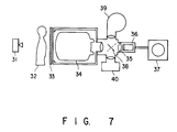
- Fig. 7 is a view showing a fluoroscopic/indirect photographic type X-ray photographic system.
- an X-ray is emitted from an X-ray tube 31 onto an object 32 to be examined.
- the X-ray passes through the object 32 to form an X-ray fluoroscopic image.
- This X-ray fluoroscopic image passes through an X-ray grid 33, so that scattered X-rays are eliminated.
- the resultant X-ray is incident on an X-ray imaging tube (X-ray image intensifier) 34.
- the X-ray fluoroscopic image is converted into a visible image by the X-ray imaging tube 34. If this system is a fluoroscopic system, the visible image passes through a TV lens 35 and is picked up by a TV camera 36. As a result, an X-ray fluoroscopic image is output to a TV monitor 37.
- this system is an indirect photographic system
- 90% of the total light amount of the image are supplied to a movie camera 39 through a half mirror 38, and the remaining 10% light amount is supplied to the TV camera 36 to output the X-ray fluoroscopic image on the TV monitor 37.
- the half mirror is reversed so that 90% light is supplied to a spot camera 40, so that the X-ray fluoroscopic image is printed on a roll or cut film.
- the X-ray imaging tube can be combined with a high-sensitivity image pickup element to constitute an X-ray photographic system (Fig. 7) having an S/N ratio equal to that of the conventional system and a high resolution.
- the X-ray imaging tube of the present invention since the light-absorbing layers having a higher concentration of a light-absorbing element on the outer surfaces thereof than that in the interiors and containing a compound of this element are formed on the side surfaces of the adjacent columnar crystals of the phosphor constituting the input phosphor screen, lateral light scattering can be suppressed, and the resolution can be increased. In addition, since no light-absorbing layer is formed on the surface of each columnar crystal which contacts the continuous phosphor layer, the luminous efficacy and luminance are not greatly decreased.
Landscapes
- Image-Pickup Tubes, Image-Amplification Tubes, And Storage Tubes (AREA)
- Apparatus For Radiation Diagnosis (AREA)
- Formation Of Various Coating Films On Cathode Ray Tubes And Lamps (AREA)
Applications Claiming Priority (4)
| Application Number | Priority Date | Filing Date | Title |
|---|---|---|---|
| JP12017891 | 1991-05-24 | ||
| JP120178/91 | 1991-05-24 | ||
| JP12077592A JP3297078B2 (ja) | 1991-05-24 | 1992-05-13 | X線イメージ管およびその製造方法 |
| JP120775/92 | 1992-05-13 |
Publications (2)
| Publication Number | Publication Date |
|---|---|
| EP0514921A1 true EP0514921A1 (de) | 1992-11-25 |
| EP0514921B1 EP0514921B1 (de) | 1996-07-17 |
Family
ID=26457801
Family Applications (1)
| Application Number | Title | Priority Date | Filing Date |
|---|---|---|---|
| EP92108674A Expired - Lifetime EP0514921B1 (de) | 1991-05-24 | 1992-05-22 | Röntgenbildröhre |
Country Status (4)
| Country | Link |
|---|---|
| US (2) | US5338926A (de) |
| EP (1) | EP0514921B1 (de) |
| JP (1) | JP3297078B2 (de) |
| DE (1) | DE69212231T2 (de) |
Cited By (2)
| Publication number | Priority date | Publication date | Assignee | Title |
|---|---|---|---|---|
| EP0667635A1 (de) * | 1994-02-09 | 1995-08-16 | Koninklijke Philips Electronics N.V. | Bildverstärkerröhre |
| WO2002048739A3 (de) * | 2000-12-11 | 2002-09-19 | Agfa Gevaert Ag | Speicherschicht und wandlungsschicht sowie vorrichtung zum auslesen von röntgeninformationen und röntgenkassette |
Families Citing this family (13)
| Publication number | Priority date | Publication date | Assignee | Title |
|---|---|---|---|---|
| US5646477A (en) * | 1993-03-17 | 1997-07-08 | Kabushiki Kaisha Toshiba | X-ray image intensifier |
| DE19516450C1 (de) * | 1995-05-04 | 1996-08-08 | Siemens Ag | Verfahren und Vorrichtung zum Herstellen einer Leuchtschicht aus Cesiumiodid-Thallium auf einem Substrat in einer Bedampfungsanlage |
| JPH0998970A (ja) * | 1995-10-06 | 1997-04-15 | Canon Inc | X線撮像装置 |
| WO1999022394A1 (en) * | 1997-10-27 | 1999-05-06 | Evgeny Invievich Givargizov | Cathodoluminescent screen with a columnar structure, and the method for its preparation |
| US7091501B2 (en) * | 2002-03-08 | 2006-08-15 | Agfa-Gevaert | Binderless storage phosphor screen on a dedicated support |
| US6977385B2 (en) * | 2002-03-26 | 2005-12-20 | Agfa-Gevaert | Storage phosphor screen having binderless colored layers |
| JP2006098241A (ja) * | 2004-09-29 | 2006-04-13 | Fuji Photo Film Co Ltd | 放射線像変換パネル |
| CN102725658B (zh) * | 2010-01-28 | 2014-09-03 | 佳能株式会社 | 闪烁体结晶体、其制造方法和放射线检测器 |
| JP2012098175A (ja) * | 2010-11-02 | 2012-05-24 | Sony Corp | 放射線検出素子およびその製造方法、放射線検出モジュール並びに放射線画像診断装置 |
| JP5456013B2 (ja) * | 2010-12-17 | 2014-03-26 | 富士フイルム株式会社 | 放射線撮像装置 |
| JP5460572B2 (ja) | 2010-12-27 | 2014-04-02 | 富士フイルム株式会社 | 放射線画像検出装置及びその製造方法 |
| JP5121960B2 (ja) * | 2011-03-30 | 2013-01-16 | キヤノン株式会社 | 相分離構造を有するシンチレータ結晶体 |
| JP6442988B2 (ja) * | 2014-10-31 | 2018-12-26 | コニカミノルタ株式会社 | X線耐久性劣化機能を有するシンチレータ、および該シンチレータを有する放射線検出器、並びにこれらの製造方法 |
Citations (2)
| Publication number | Priority date | Publication date | Assignee | Title |
|---|---|---|---|---|
| EP0283020A2 (de) * | 1987-03-18 | 1988-09-21 | Kabushiki Kaisha Toshiba | Photokathode und ihr Herstellungsverfahren |
| US4803366A (en) * | 1985-08-23 | 1989-02-07 | Gerard Vieux | Input screen scintillator for a radiological image intensifier tube and a method of manufacturing such a scintillator |
Family Cites Families (12)
| Publication number | Priority date | Publication date | Assignee | Title |
|---|---|---|---|---|
| US3089956A (en) * | 1953-07-10 | 1963-05-14 | Westinghouse Electric Corp | X-ray fluorescent screen |
| US3482104A (en) * | 1965-05-24 | 1969-12-02 | Jack Finkle | System for televising radiant energy images employing image transducer device with radiant energy image responsive photocathode |
| FR2360989A1 (fr) * | 1976-08-03 | 1978-03-03 | Thomson Csf | Intensificateur d'image radiologique, et son procede de fabrication |
| JPS5440071A (en) * | 1977-09-05 | 1979-03-28 | Sharp Corp | Electronic timer device |
| US4479061A (en) * | 1980-07-25 | 1984-10-23 | Canon Kabushiki Kaisha | Luminance amplifier and an apparatus including the same |
| JPS59121733A (ja) * | 1982-12-28 | 1984-07-13 | Yoshihiro Hamakawa | X線イメ−ジ管入力面の製造方法 |
| JPS59121737A (ja) * | 1982-12-28 | 1984-07-13 | Yoshihiro Hamakawa | X線イメ−ジ管の入力面 |
| JPS6243046A (ja) * | 1985-08-19 | 1987-02-25 | Toshiba Corp | X線イメ−ジ管の入力面 |
| US4739172A (en) * | 1986-01-08 | 1988-04-19 | Tokyo Shibaura Denki Kabushiki Kaisha | Fiber optic phosphor screen and a method of manufacturing the same |
| JPS63228728A (ja) * | 1987-03-18 | 1988-09-22 | Sumitomo Electric Ind Ltd | 半導体チツプのダイボンデイング装置 |
| FR2623659B1 (fr) * | 1987-11-24 | 1990-03-09 | Labo Electronique Physique | Tube intensificateur d'images a rayons x |
| JP2996711B2 (ja) * | 1990-10-18 | 2000-01-11 | 株式会社東芝 | X線イメージ管及びその製造方法 |
-
1992
- 1992-05-13 JP JP12077592A patent/JP3297078B2/ja not_active Expired - Fee Related
- 1992-05-22 DE DE69212231T patent/DE69212231T2/de not_active Expired - Fee Related
- 1992-05-22 EP EP92108674A patent/EP0514921B1/de not_active Expired - Lifetime
- 1992-05-22 US US07/886,824 patent/US5338926A/en not_active Expired - Lifetime
-
1994
- 1994-02-28 US US08/202,466 patent/US5445846A/en not_active Expired - Lifetime
Patent Citations (2)
| Publication number | Priority date | Publication date | Assignee | Title |
|---|---|---|---|---|
| US4803366A (en) * | 1985-08-23 | 1989-02-07 | Gerard Vieux | Input screen scintillator for a radiological image intensifier tube and a method of manufacturing such a scintillator |
| EP0283020A2 (de) * | 1987-03-18 | 1988-09-21 | Kabushiki Kaisha Toshiba | Photokathode und ihr Herstellungsverfahren |
Non-Patent Citations (3)
| Title |
|---|
| DATABASE WPI Week 7635, Derwent Publications Ltd., London, GB; AN 76-65736 & JP-A-51 080 690 (TOKYO SHIBAURA) * |
| JOURNAL OF CRYSTAL GROWTH vol. 7, 1970, pages 259 - 261 M.JOSE YACAMAN ET AL. 'Growth of Mn2O3 thin films by impurity diffusion from volume to surface in impure NaCl crystals' * |
| PATENT ABSTRACTS OF JAPAN vol. 8, no. 239 (E-276)(1676) 2 November 1984 & JP-A-59 121 733 ( Y. HAMAKAWA ) 13 July 1984 * |
Cited By (4)
| Publication number | Priority date | Publication date | Assignee | Title |
|---|---|---|---|---|
| EP0667635A1 (de) * | 1994-02-09 | 1995-08-16 | Koninklijke Philips Electronics N.V. | Bildverstärkerröhre |
| BE1008070A3 (nl) * | 1994-02-09 | 1996-01-09 | Philips Electronics Nv | Beeldversterkerbuis. |
| WO2002048739A3 (de) * | 2000-12-11 | 2002-09-19 | Agfa Gevaert Ag | Speicherschicht und wandlungsschicht sowie vorrichtung zum auslesen von röntgeninformationen und röntgenkassette |
| US7109496B2 (en) | 2000-12-11 | 2006-09-19 | Agfa-Gevaert Healthcare Gmbh | Storage layer, conversion layer and a device for reading x-ray information, in addition to an x-ray cassette |
Also Published As
| Publication number | Publication date |
|---|---|
| DE69212231D1 (de) | 1996-08-22 |
| JP3297078B2 (ja) | 2002-07-02 |
| US5445846A (en) | 1995-08-29 |
| JPH05174747A (ja) | 1993-07-13 |
| DE69212231T2 (de) | 1996-12-05 |
| EP0514921B1 (de) | 1996-07-17 |
| US5338926A (en) | 1994-08-16 |
Similar Documents
| Publication | Publication Date | Title |
|---|---|---|
| EP0514921B1 (de) | Röntgenbildröhre | |
| US5594253A (en) | Hybrid luminescent device for imaging of ionizing and penetrating radiation | |
| US4297584A (en) | Rare earth phosphors and phosphor screens | |
| CN1276269C (zh) | 固态x光探测器 | |
| DE69726080T2 (de) | Photokathode und solche Kathode enthaltende Elektronenröhre | |
| WO2004029657A1 (ja) | 放射線検出器用蛍光体シートおよびそれを用いた放射線検出器と放射線検査装置 | |
| US3693018A (en) | X-ray image intensifier tubes having the photo-cathode formed directly on the pick-up screen | |
| EP0283020B1 (de) | Photokathode und ihr Herstellungsverfahren | |
| EP0667635B1 (de) | Bildverstärkerröhre | |
| CN87102131A (zh) | 辐射转换屏幕 | |
| EP0240951B1 (de) | Röntgenstrahlenbildverstärker | |
| EP0197597B1 (de) | Mit einer die Sekundärstrahlung absorbierende lumineszierenden Schicht versehene Röntgenbildverstärkerröhre | |
| JP4764039B2 (ja) | 放射線検出器用蛍光体シートおよびそれを用いた放射線検出器 | |
| CN1130794A (zh) | 辐射换能器中具有针状组织的闪烁体 | |
| EP0282089B1 (de) | Röntgenbildverstärker | |
| JPH0636715A (ja) | X線イメージ管 | |
| WO2018110061A1 (ja) | シンチレータプレート、放射線検出装置および放射線検出システム | |
| JPH0636717A (ja) | X線イメージ管 | |
| JP2575359B2 (ja) | X線イメ−ジインテンシフアイア | |
| JPH0636716A (ja) | X線イメージ管およびその製造方法 | |
| JP2695820B2 (ja) | 光電面及びその形成方法 | |
| JPH11500857A (ja) | X線検出器 | |
| CN1051871C (zh) | X射线图像管及其制造方法 | |
| Beauvais et al. | New progress in high-performance x-ray image intensifiers | |
| JPH04154032A (ja) | X線蛍光増倍管及びその製造方法 |
Legal Events
| Date | Code | Title | Description |
|---|---|---|---|
| PUAI | Public reference made under article 153(3) epc to a published international application that has entered the european phase |
Free format text: ORIGINAL CODE: 0009012 |
|
| 17P | Request for examination filed |
Effective date: 19920619 |
|
| AK | Designated contracting states |
Kind code of ref document: A1 Designated state(s): DE FR GB NL |
|
| K1C1 | Correction of patent application (title page) published |
Effective date: 19921125 |
|
| 17Q | First examination report despatched |
Effective date: 19941221 |
|
| GRAH | Despatch of communication of intention to grant a patent |
Free format text: ORIGINAL CODE: EPIDOS IGRA |
|
| GRAH | Despatch of communication of intention to grant a patent |
Free format text: ORIGINAL CODE: EPIDOS IGRA |
|
| GRAA | (expected) grant |
Free format text: ORIGINAL CODE: 0009210 |
|
| AK | Designated contracting states |
Kind code of ref document: B1 Designated state(s): DE FR GB NL |
|
| REF | Corresponds to: |
Ref document number: 69212231 Country of ref document: DE Date of ref document: 19960822 |
|
| ET | Fr: translation filed | ||
| PLBE | No opposition filed within time limit |
Free format text: ORIGINAL CODE: 0009261 |
|
| STAA | Information on the status of an ep patent application or granted ep patent |
Free format text: STATUS: NO OPPOSITION FILED WITHIN TIME LIMIT |
|
| 26N | No opposition filed | ||
| REG | Reference to a national code |
Ref country code: GB Ref legal event code: 746 Effective date: 19981012 |
|
| REG | Reference to a national code |
Ref country code: FR Ref legal event code: D6 |
|
| REG | Reference to a national code |
Ref country code: GB Ref legal event code: IF02 |
|
| PGFP | Annual fee paid to national office [announced via postgrant information from national office to epo] |
Ref country code: DE Payment date: 20080529 Year of fee payment: 17 |
|
| PGFP | Annual fee paid to national office [announced via postgrant information from national office to epo] |
Ref country code: NL Payment date: 20080501 Year of fee payment: 17 |
|
| PGFP | Annual fee paid to national office [announced via postgrant information from national office to epo] |
Ref country code: GB Payment date: 20080528 Year of fee payment: 17 |
|
| REG | Reference to a national code |
Ref country code: FR Ref legal event code: ST Effective date: 20090119 |
|
| PG25 | Lapsed in a contracting state [announced via postgrant information from national office to epo] |
Ref country code: FR Free format text: LAPSE BECAUSE OF NON-PAYMENT OF DUE FEES Effective date: 20080602 |
|
| REG | Reference to a national code |
Ref country code: FR Ref legal event code: D3 |
|
| GBPC | Gb: european patent ceased through non-payment of renewal fee |
Effective date: 20090522 |
|
| NLV4 | Nl: lapsed or anulled due to non-payment of the annual fee |
Effective date: 20091201 |
|
| PG25 | Lapsed in a contracting state [announced via postgrant information from national office to epo] |
Ref country code: NL Free format text: LAPSE BECAUSE OF NON-PAYMENT OF DUE FEES Effective date: 20091201 |
|
| REG | Reference to a national code |
Ref country code: FR Ref legal event code: ST Effective date: 20100129 |
|
| PGFP | Annual fee paid to national office [announced via postgrant information from national office to epo] |
Ref country code: FR Payment date: 20080514 Year of fee payment: 17 |
|
| PG25 | Lapsed in a contracting state [announced via postgrant information from national office to epo] |
Ref country code: GB Free format text: LAPSE BECAUSE OF NON-PAYMENT OF DUE FEES Effective date: 20090522 |
|
| PG25 | Lapsed in a contracting state [announced via postgrant information from national office to epo] |
Ref country code: DE Free format text: LAPSE BECAUSE OF NON-PAYMENT OF DUE FEES Effective date: 20091201 |
|
| PGRI | Patent reinstated in contracting state [announced from national office to epo] |
Ref country code: FR Effective date: 20090414 |
|
| PG25 | Lapsed in a contracting state [announced via postgrant information from national office to epo] |
Ref country code: FR Free format text: LAPSE BECAUSE OF NON-PAYMENT OF DUE FEES Effective date: 20090531 |