EP0515533B1 - Affichage tridimensionnel - Google Patents
Affichage tridimensionnel Download PDFInfo
- Publication number
- EP0515533B1 EP0515533B1 EP91905003A EP91905003A EP0515533B1 EP 0515533 B1 EP0515533 B1 EP 0515533B1 EP 91905003 A EP91905003 A EP 91905003A EP 91905003 A EP91905003 A EP 91905003A EP 0515533 B1 EP0515533 B1 EP 0515533B1
- Authority
- EP
- European Patent Office
- Prior art keywords
- display
- layers
- liquid crystal
- display material
- visual state
- Prior art date
- Legal status (The legal status is an assumption and is not a legal conclusion. Google has not performed a legal analysis and makes no representation as to the accuracy of the status listed.)
- Expired - Lifetime
Links
Images


Classifications
-
- G—PHYSICS
- G02—OPTICS
- G02B—OPTICAL ELEMENTS, SYSTEMS OR APPARATUS
- G02B30/00—Optical systems or apparatus for producing three-dimensional [3D] effects, e.g. stereoscopic images
- G02B30/50—Optical systems or apparatus for producing three-dimensional [3D] effects, e.g. stereoscopic images the image being built up from image elements distributed over a three-dimensional [3D] volume, e.g. voxels
- G02B30/52—Optical systems or apparatus for producing three-dimensional [3D] effects, e.g. stereoscopic images the image being built up from image elements distributed over a three-dimensional [3D] volume, e.g. voxels the three-dimensional [3D] volume being constructed from a stack or sequence of two-dimensional [2D] planes, e.g. depth sampling systems
-
- G—PHYSICS
- G02—OPTICS
- G02F—OPTICAL DEVICES OR ARRANGEMENTS FOR THE CONTROL OF LIGHT BY MODIFICATION OF THE OPTICAL PROPERTIES OF THE MEDIA OF THE ELEMENTS INVOLVED THEREIN; NON-LINEAR OPTICS; FREQUENCY-CHANGING OF LIGHT; OPTICAL LOGIC ELEMENTS; OPTICAL ANALOGUE/DIGITAL CONVERTERS
- G02F1/00—Devices or arrangements for the control of the intensity, colour, phase, polarisation or direction of light arriving from an independent light source, e.g. switching, gating or modulating; Non-linear optics
- G02F1/01—Devices or arrangements for the control of the intensity, colour, phase, polarisation or direction of light arriving from an independent light source, e.g. switching, gating or modulating; Non-linear optics for the control of the intensity, phase, polarisation or colour
- G02F1/13—Devices or arrangements for the control of the intensity, colour, phase, polarisation or direction of light arriving from an independent light source, e.g. switching, gating or modulating; Non-linear optics for the control of the intensity, phase, polarisation or colour based on liquid crystals, e.g. single liquid crystal display cells
- G02F1/133—Constructional arrangements; Operation of liquid crystal cells; Circuit arrangements
- G02F1/1333—Constructional arrangements; Manufacturing methods
- G02F1/1347—Arrangement of liquid crystal layers or cells in which the final condition of one light beam is achieved by the addition of the effects of two or more layers or cells
-
- H—ELECTRICITY
- H04—ELECTRIC COMMUNICATION TECHNIQUE
- H04N—PICTORIAL COMMUNICATION, e.g. TELEVISION
- H04N13/00—Stereoscopic video systems; Multi-view video systems; Details thereof
- H04N13/30—Image reproducers
- H04N13/388—Volumetric displays, i.e. systems where the image is built up from picture elements distributed through a volume
- H04N13/395—Volumetric displays, i.e. systems where the image is built up from picture elements distributed through a volume with depth sampling, i.e. the volume being constructed from a stack or sequence of two-dimensional [2D] image planes
-
- G—PHYSICS
- G02—OPTICS
- G02F—OPTICAL DEVICES OR ARRANGEMENTS FOR THE CONTROL OF LIGHT BY MODIFICATION OF THE OPTICAL PROPERTIES OF THE MEDIA OF THE ELEMENTS INVOLVED THEREIN; NON-LINEAR OPTICS; FREQUENCY-CHANGING OF LIGHT; OPTICAL LOGIC ELEMENTS; OPTICAL ANALOGUE/DIGITAL CONVERTERS
- G02F1/00—Devices or arrangements for the control of the intensity, colour, phase, polarisation or direction of light arriving from an independent light source, e.g. switching, gating or modulating; Non-linear optics
- G02F1/01—Devices or arrangements for the control of the intensity, colour, phase, polarisation or direction of light arriving from an independent light source, e.g. switching, gating or modulating; Non-linear optics for the control of the intensity, phase, polarisation or colour
- G02F1/13—Devices or arrangements for the control of the intensity, colour, phase, polarisation or direction of light arriving from an independent light source, e.g. switching, gating or modulating; Non-linear optics for the control of the intensity, phase, polarisation or colour based on liquid crystals, e.g. single liquid crystal display cells
- G02F1/133—Constructional arrangements; Operation of liquid crystal cells; Circuit arrangements
- G02F1/1333—Constructional arrangements; Manufacturing methods
- G02F1/1347—Arrangement of liquid crystal layers or cells in which the final condition of one light beam is achieved by the addition of the effects of two or more layers or cells
- G02F1/13476—Arrangement of liquid crystal layers or cells in which the final condition of one light beam is achieved by the addition of the effects of two or more layers or cells in which at least one liquid crystal cell or layer assumes a scattering state
Definitions
- This invention relates to a display a presenting three dimensional visual effect.
- a number of three-dimensional (3D) displays are known. They may be broadly classified into two types: (1) fixed viewing direction ones and (2) real 3D image ones.
- a fixed viewing direction display the 3D image is viewed from one direction only -- when the viewer moves around the displayed image, the image does not change.
- Perspective and binocular displays are examples of fixed viewing direction displays.
- a real 3D image display permits the viewer to have a side view of the object when moving around the image. That is, the 3D effect is preserved even when the viewer changes the viewing angle.
- Holography, internal photography, and varifocal mirror displays generate real 3D images.
- JP-A-62-235929 discloses a device comprising a plurality of liquid crystal cells which allows to display a real 3D image.
- Tamura et al., Applied Optics 21(20), 3659 (1982), disclose a multilayer 3D display comprising multiple layers of images, in which each image layer is placed at a different optical path length position from a viewing window by a multidirectional beam splitter, to show a composite 3D image.
- a light reflecting 3D display system discloses a light reflecting 3D display system.
- a light source provides a sequence of images, each representing a different depth plane of a subject.
- Each of the images is selectively reflected from one of a plurality of differently positioned light direction modulators, to synthesize a 3D image of the subject.
- Ruderfer, US 2,749,480 (1956), discloses an apparatus for producing 3D visual patterns.
- the apparatus comprises a plurality of illuminable points or zones determining a cubical or spherical volume.
- the light points are equipped with electrically operated lamp means and switch means for selectively choosing the lamp means to be actuated.
- Fergason discloses a complementary color display device having color layers of encapsulated liquid crystal material, so that light reaching an observer's eyes passes through the layers. By selectively switching the transparency of the colored layers, the observed light is colored or not.
- Aizawa discloses a multilayered matrix-type liquid crystal display, comprising front and rear substrates and at least one intermediate substrate interposed therebetween, with liquid crystal layers interposed between the substrates. Switching of the liquid crystal material is effected by intersecting signal and scanning electrodes arranged on opposed mutually facing surfaces of the intermediate and rear substrate and of the intermediate and front substrate. Color layers are arranged in an optical path corresponding to the intersecting portions of the signal and scanning electrodes, but on the opposite side of the intermediate substrate on which the associated intersecting signal and scanning lines are located.
- Each colored unit includes either a standard liquid crystal display unit and a colored polarized filter, or a dichroic liquid crystal display unit. By selectively energizing one or more of the liquid crystal displays, display characters of varying colors can be produced.
- Benton discloses a multi-band liquid crystal film for visual observation of two or more patterns, prepared by laminating at least two polyurethane films, each containing discrete aggregates of liquid crystals against a black film, such that the visual response of the liquid crystals of each succeeding film is different from that of the other films.
- the prior art 3D display devices are disadvantageous in that they are rather bulky, and require expensive optics. I have made a three dimensional display device which can generate real 3D images without the need for special glasses or other visual aids, but which is compact and simple to construct.
- the device of this invention is dynamic, as opposed to static; that is, it can present different 3D images, or even moving 3D images in real time.
- This invention provides a display device as defined by claim 1.
- Figures 1 and 1a depict schematically in cross-section an encapsulated liquid crystal material which can be used for devices of this invention.
- Figures 2a-c depict various electrode patterns for addressing the display material.
- Figures 3 and 3a depict another addressing scheme, this one using multiplexed active matrix elements.
- Figures 4a and 4b depict schematically how the multiple layers of display material in this invention are used to form an image having presenting a three-dimensional visual effect.
- Figure 5 depicts schematically a multiple layer construction, with spacers, for a display of this invention.
- Figure 6 depicts another preferred multiple layer construction.
- the pixels in the display material are switched from the first visual state to the second visual state by the application or removal of an electric field or by the passage of current.
- the pixels in the first visual state the pixels may be nontransparent -- strongly absorb and/or scatter incident light, or interact with incident light so as to cause it to be absorbed by associated elements such as polarizers -- while in the second visual state the pixels may be substantially transparent, permitting the incident light to be reflected back to the viewer by a reflector located behind them or permitting, in the case of a back-lit display, that light pass through the display and reach the viewer.
- the layers of display material comprise an encapsulated liquid crystal material, whose preparation is disclosed in U.S. Pat. Nos. 4,435,047 (1984), 4,606,611 (1986), 4,616,903 (1986), and 4,707,080 (1987), all to Fergason; published European patent application EP 156,615 (1985), by Pearlman et al.; U.S. Pat. No. 4,671,618 (1987), to Wu et al.; U.S. Pat. Nos. 4,673,255 (1987) and 4,685,771 (1987), to West et al.; and U.S. Pat. No.
- Liquid crystals denotes a composition having liquid crystalline properties, whether that composition is a single discrete liquid crystalline compound, a mixture of different liquid crystalline compounds, or a mixture of liquid crystalline and non-liquid crystalline compounds.
- Liquid crystals have typically elongated molecular shapes, with a tendency to align or orient themselves with their long molecular axes parallel to each other.
- This alignment causes liquid crystals to be anisotropic, meaning that their measured physical, optical, and other properties are dependent on the direction of measurement (parallel or perpendicular to the direction of alignment).
- the alignment direction can be influenced by an external stimulus, such as an electrical or magnetic field, causing the liquid crystals to exhibit a particular value of a physical characteristic in one direction when the stimulus is absent, but rapidly switching to a different value when the stimulus is applied. It is because of their anisotropy and their ready realignment that liquid crystals are useful as materials for displays.
- the containment medium is preferably a polymeric material.
- Suitable containment media include but are not limited to poly(vinyl alcohol), polyurethane, acrylic and methacrylic polymers and copolymers, epoxies, polyoelfins, vinyl polymers, and the like.
- Encapsulated liquid crystal material can be formed by deposition from an emulsion containing both the containment medium and liquid crystals or by the evaporation of liquid from a solution containing both containment medium and liquid crystals. It can also be formed by making an initially homogeneous mixture containing both containment medium and liquid crystals at an elevated temperature, then cooling to phase-separate out liquid crystal volumes contained in the containment medium. Further, it can be formed by an in-situ polymerization process, in which the containment medium is polymerized and simultaneously encapsulates liquid crystal material. The liquid crystal need not be entirely surrounded by the polymer, and may exist as part of a system with co-continuous phases.
- the encapsulated liquid crystal material is substantially non-transparent in the absence of a sufficient electric field (the "field-off” state) and substantially transparent in the presence of a sufficient electric field (or "field-on” state).
- the electric field induces a change in the alignment of the liquid crystals, in turn causing the encapsulated liquid crystal material to switch from a highly light-scattering (and/or absorbent) state to a highly non-scattering and substantially transparent state.
- the liquid crystals have a positive dielectric anisotropy and that the ordinary index of refraction of the liquid crystals be matched with the refractive index of the containment medium, while the extraordinary index of refraction is substantially mismatched therewith.
- Pleochroic dyes have been mixed with liquid crystals to form a solution therewith.
- the molecules of pleochroic dyes generally align with the molecules of liquid crystals, so that the application of the electric field affects not only the predominant alignment of the liquid crystals, but also of the pleochroic dye.
- the extent of the absorption of incident light by the pleochroic dye depends on its orientation relative to the incident light, the application of an external stimulus to a liquid crystal-pleochroic dye combination also provides a means for the controlled attenuation of light.
- liquid crystals also means, in context, liquid crystals containing pleochroic dye dissolved therein.
- Pleochroic dyes may be used in encapsulated liquid crystals, as described in the aforementioned Fergason patents, or in non-encapsulated systems, as described in Goldmacher et al., US 3,499,702 (1970) and Heilmeier, US 3,551,026 (1970).
- color images can be created by using pleochroic dyes, with arrays of individually colored pixels within each layer being created by selective deposition, for example by screen printing.
- a layer capable of displaying colored images can be formed by depositing side by side red, blue, and green pixels.
- the pixels need not be colored, and can simply switch between a substantially transparent state and a substantially non-transparent state which is black or gray.
- a substantially transparent state which is black or gray.
- at least two of the display material layers are the same; that is, have pixels with the same chromatic characteristics - all black-and-white pixels, all pixels of the same color, or the same groupings of red, green, and blue pixels. More preferably, each of the display material layers in the display are the same.
- the means for applying the electric field and switching each pixel from its substantially non-transparent state to its substantially transparent state may be various.
- the display material has an electrically conductive material or electrode on either side. The application of a sufficient voltage across the two electrodes then induces a corresponding change in the visual appearance of the display material between the electrodes.
- Each pixel is defined by the area of overlap between the two electrodes.
- Direct addressing meaning there is one independently addressable line for each pixel, may be used.
- Multiplexing combining rows of independently addressable strips of electrode material on one side of the display material and columns of independently addressable strips of electrode material on the other side, may also be used.
- Active matrix addressing utilizing non-linear electrical devices at each pixel, represents yet another way of addressing the pixels. Suitable active matrix devices include transistors (particularly thin-film transistors or TFT's), back-to-back diodes, metal-insulator-metal (or MIM) devices, and varistors.
- encapsulated liquid crystal material 10 comprising a containment medium 11 containing discrete volumes of liquid crystals 12.
- Transparent support materials 13 and 14 (made of, for example, glass, plexiglass, or a polyester such as polyethylene terephthalate) provide support for the encapsulated liquid crystal material 10 and electrodes 15 and 16.
- Electrode 15 is a ground plane electrode substantially coextensive with the encapsulated liquid crystal material, while electrodes 16 are patterned in a desired pattern. Each pixel is defined by the overlap between electrode 15 and the corresponding electrode 16, as illustrated in one instance by dotted reference lines 17a and 17b.
- Electrodes 15 and 16 may be made of a transparent electrically conductive material, such as indium tin oxide (ITO) or a vapor deposited thin coating of a metal such as nickel or gold.
- ITO indium tin oxide
- a metal such as nickel or gold.
- the top electrode 15 may also be patterned, as illustrated in Fig. la. In this figure, the top electrode is now depicted as a pattern of electrodes 15. Numerals 10, 11, 12, 13, 14, 16, and 17a-b retain the same significance as in Fig. 1.
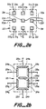
- Fig. 2a-c depict some common electrode patterns.
- Fig. 2a there is depicted a regular array 20 of electrodes 21a-i, each addressed by its own lead 22a-i, respectively.
- Fig. 2b depicts the familiar seven-segment figure-eight pattern 23 found in watches, calculators and other devices requiring a digital numerical display.
- Each of segments 24a-g is addressed by its own lead 25a-g, respectively.
- any of the numerals 0-9 may be displayed.
- any other pattern or shaped picture element may be used to represent a portion of a three dimensional object. While Fig. 2a and 2b use a direct addressing Fig.
- FIG. 2c depicts an electrode pattern 26 in which multiplexing is used. Rows of top electrodes 27a-c, each connected to respective leads 28a-c, are superimposed on columns of bottom electrodes 29a-c.
- By the application of a voltage across selected top and bottom electrodes particular pixels, defined by the overlap between the electrodes, can be switched. For example, by application of a voltage across electrodes 27a and 29a, pixel 31 can be switched, while by the application of a voltage across electrodes 27c and 29b, pixel 32 can be switched.
- an array of multiplexed active matrix devices may be employed. Such a scheme is illustrated in Fig. 3, in an exploded view, with TFT's as the active matrix devices.
- Fig. 3 depicts a sandwich 40 of encapsulated liquid crystal material 41 between a first support material 43 coated with a transparent ground plane electrode 42 (made for example from ITO) and a second support material 45 (typically glass) having thereon an array 44 of multiplexed TFT's.
- the construction of the array is shown in greater detail in Fig. 3a, corresponding to a magnification of the portion of Fig. 3 labeled A.
- Each pixel is defined by an electrode 46 (made for example from ITO).
- the application of a voltage across each electrode 46 is controlled by a TFT 47.
- each TFT is address in a multiplexed fashion via scan line 49 and data line 48.
- FIGS 4a-4b The manner in which the three-dimensional visual effect is achieved by the display of this invention is shown schematically in Figures 4a-4b. Seven layers of display material 51a-g, which are independently addressable by a means such as described hereinabove, have selected portions 50a-g in the opaque state (that is, in the field-off state, if the display material is an encapsulated liquid crystal material, to form the image of a cone. The balance of the display material is in a transparent (field-on) state. An observer can see through to the bottom layers where the display material is transparent. Although in Figures 4a-b the observer is shown viewing the display from above, a three dimensional effect can also be obtained by viewing from below. When viewed from oblique angles, the three-dimensional perspective is maintained, allowing the observer to inspect the cone from different orientations. The relative dimensions of the displayed object will remain true at all viewing angles, eliminating the distortions seen in conventional three-dimensional displays.
- the minimum number of layers of display material is two, but preferably there are at least four, more preferably at least eight layers.
- a desirable number of layers, from the viewpoint of providing an attractive 3D effect but yet keeping the device relatively simple, is between 4 and 20.
- the stacked multiple layers of the display material can be almost touching, or spaced apart. It is generally desirable to space the layers apart in order to maximize parallax and consequently the three-dimensional effect. Where the device has less than four layers, it is especially important to keep the spacing between adjacent layers sufficiently large to provide a sufficient parallax effect. Accordingly, in such embodiments the spacing between adjacent layers are preferably at least equal to the smallest average dimension of the pixels. The separation between the adjacent layers is preferably at least 0.5 mm, more preferably at least 1 mm.
- the spacing means may perform the additional function of being a substrate or supporting means for the display material and/or the electrodes or other electronic components for addressing the display material. Naturally, in order to permit viewing of the lower layers of display material, the spacing means should be substantially transparent.
- the spacing means does not physically span all the gaps between adjacent layers, but is instead positioned only along the edges or at selected intervals, with the space in between filled with air or other suitable filler material.
- the refractive index of the spacing means of the filler material is substantially equal (preferably within ⁇ 0.05) to the refractive index of the display material or to the refractive index of the materials which it contacts -- e.g., the support materials 56a-b and 57 a-b of Fig. 5, discussed below -- to minimize reflection losses through the layers and/or distortion due to refraction.
- Silicone oil and other viscous, clear liquids are preferred filler material in those embodiments in which the display material is encapsulated liquid crystal material.
- Other preferred materials are pressure sensitive adhesives and clear gels.
- FIG. 5 shows an embodiment having filler materials between adjacent layers. For simplicity, only two layers of display material are shown, but additional layers may be constructed in like fashion.
- Display material layers 55a-b are sandwiched between support materials 56a-b and 57a-b, made for example from glass, plexiglass, or poly(ethylene terephthalate (PET)).
- Support materials 56a-b are coated with unpatterned transparent electrodes 58a-b (made for example from ITO), as ground plane electrodes, on the side facing the display material.
- Support materials 57a-b are coated with patterned electrodes 59a-b, also permissibly made from ITO.
- a spacing material 60 which can be made from plexiglass, is located between the two layers.
- refractive index matching spacer materials 61a-b e.g., silicone oil
- Transparent material 65 is coated on either side with unpatterned transparent electrodes 66a-b, which serve as ground plane electrodes. These electrodes contact display materials 67a-b, respectively, which in turn, on their other sides are contacted by patterned electrodes 68a-b supported by support materials 69a-b.
- the displayed three dimensional images can be static, or can be moving images, the movement of the image being created by addressing different sets of pixels at different times. With encapsulated liquid crystals the switching times can be less than 30 milliseconds, providing flicker-free video type movement in the three dimensional image.
- Lenticular screens or other lenses can be used in conjunction with the display to enhance the visual experience.
- Displays which require polarizers for example of the twisted nematic liquid crystal type, can be used, although they are not preferred. This is because even in the transparent state the polarizer will pass through only 50% of the incident unpolarized light. Additional losses may occur when the light passes through subsequent polarizers. If a twisted nematic construction is employed, the polarizers in successive layers should be all aligned parallel to each other, to minimize the attenuation of light by the polarizers. Further, twisted nematic displays generally have a reflector at their back, in which case the reflector should not randomize the polarization of light passing through the layers of display material above it. The reflector can be a specular reflector.
- the display can be illuminated from the front (i.e., the same side as the observer), the edges, or the back, or all three.
- a reflector (specular, diffuse, or containing a pattern or picture) can be used behind the display.
- Embodiments employing highly absorbing display material do not work as well with front lighting as they do with back lighting. Forward scattering systems appear opaque, but actually allow significant amounts of light to pass up to subsequent layers.
- Several sources of light can be used concurrently. The lights can be directed towards specific portions of the display, enhancing contrast and/or the 3D effect and providing means for generating color images.
- the multiple sources of light can be brought in from front, back, or side.
- Light sources can be incandescent bulbs, lasers, arc lamps, and the like.
- the 3D effect can be in the visible region, or outside the visible region into the infra-red or near ultraviolet.
Landscapes
- Physics & Mathematics (AREA)
- Nonlinear Science (AREA)
- Optics & Photonics (AREA)
- General Physics & Mathematics (AREA)
- Multimedia (AREA)
- Crystallography & Structural Chemistry (AREA)
- Chemical & Material Sciences (AREA)
- Engineering & Computer Science (AREA)
- Mathematical Physics (AREA)
- Signal Processing (AREA)
- Liquid Crystal (AREA)
- Devices For Indicating Variable Information By Combining Individual Elements (AREA)
- Holo Graphy (AREA)
- Testing, Inspecting, Measuring Of Stereoscopic Televisions And Televisions (AREA)
- Small-Scale Networks (AREA)
- Optical Communication System (AREA)
Claims (8)
- Dispositif d'affichage à cristaux liquides agencé pour afficher une image en trois dimensions, comprenant une pluralité de couches empilées d'un matériau d'affichage à cristaux liquides et contenant une pluralité de pixels qui sont chacun indépendamment commutables entre un premier état visuel et un second état visuel, chaque couche ayant des pixels de la même couleur ou d'une même combinaison de couleurs; des moyens de commutation pour commuter indépendamment chaque pixel entre le premier état visuel et le second état visuel; et des moyens de séparation pour fournir une séparation entre des couches adjacentes de matériau d'affichage; caractérisé en ce que le matériau d'affichage consiste en un matériau à cristaux liquides enrobés, dans lequel si le nombre de couches de matériau d'affichage est inférieur à quatre, la séparation entre les couches adjacentes est d'au moins 0,5 mm, et un matériau de remplissage remplit la séparation entre les couches adjacentes de matériau d'affichage et a un indice de réfraction sensiblement égal à celui des couches adjacentes de matériau d'affichage.
- Dispositif d'affichage selon la revendication 1, dans lequel chaque pixel est directement adressé.
- Dispositif d'affichage selon la revendication 1, dans lequel chaque pixel est adressé par une matrice active.
- Dispositif d'affichage selon la revendication 3, dans lequel la matrice active comporte des transistors à film mince, des diodes montées tête-bêche, ou des MIM.
- Dispositif d'affichage selon la revendication 3, dans lequel la matrice active comporte des varistances.
- Dispositif d'affichage selon la revendication 1, dans lequel le matériau d'affichage comporte en outre un colorant pléochroïque mélangé avec les cristaux liquides.
- Dispositif d'affichage selon la revendication 1, dans lequel le dispositif d'affichage comporte au moins quatre couches de matériau d'affichage.
- Dispositif d'affichage selon la revendication 1, dans lequel le dispositif d'affichage comporte entre 4 et 20 couches de matériau d'affichage.
Applications Claiming Priority (3)
| Application Number | Priority Date | Filing Date | Title |
|---|---|---|---|
| US07/479,005 US5113272A (en) | 1990-02-12 | 1990-02-12 | Three dimensional semiconductor display using liquid crystal |
| US479005 | 1990-02-12 | ||
| PCT/US1991/000859 WO1991012554A1 (fr) | 1990-02-12 | 1991-02-07 | Affichage tridimensionnel |
Publications (2)
| Publication Number | Publication Date |
|---|---|
| EP0515533A1 EP0515533A1 (fr) | 1992-12-02 |
| EP0515533B1 true EP0515533B1 (fr) | 1995-05-03 |
Family
ID=23902263
Family Applications (1)
| Application Number | Title | Priority Date | Filing Date |
|---|---|---|---|
| EP91905003A Expired - Lifetime EP0515533B1 (fr) | 1990-02-12 | 1991-02-07 | Affichage tridimensionnel |
Country Status (7)
| Country | Link |
|---|---|
| US (1) | US5113272A (fr) |
| EP (1) | EP0515533B1 (fr) |
| JP (1) | JPH05504210A (fr) |
| AT (1) | ATE122157T1 (fr) |
| CA (1) | CA2075807A1 (fr) |
| DE (1) | DE69109471T2 (fr) |
| WO (1) | WO1991012554A1 (fr) |
Families Citing this family (163)
| Publication number | Priority date | Publication date | Assignee | Title |
|---|---|---|---|---|
| US5572375A (en) * | 1990-08-03 | 1996-11-05 | Crabtree, Iv; Allen F. | Method and apparatus for manipulating, projecting and displaying light in a volumetric format |
| US5477352A (en) * | 1990-10-31 | 1995-12-19 | Sharp Kaushiki Kaisha | Liquid crystal display device with liquid crystal dispersed or impregnated in a perfluoro-type polymer of perfluoroalkyl acrylate or methacrylate |
| US5252958A (en) * | 1991-09-05 | 1993-10-12 | Daniels John J | Method and apparatus for interspecies communication |
| JP3105311B2 (ja) * | 1991-10-08 | 2000-10-30 | 株式会社半導体エネルギー研究所 | 液晶電気光学装置およびその作製方法 |
| FR2686711A1 (fr) * | 1992-01-08 | 1993-07-30 | Terumo Corp | Appareil de visualisation d'images tridimensionnelles a echantillonnage en profondeur. |
| JP2672055B2 (ja) * | 1992-05-08 | 1997-11-05 | 信幸 山村 | 液晶表示素子とその製造方法及びこれを使用する表示装置 |
| US5414543A (en) * | 1992-08-24 | 1995-05-09 | Samsung Electronics Co., Ltd. | Method for manufacturing a multiple level liquid crystal display using alternating metal and metal oxide layers |
| KR100230354B1 (ko) * | 1992-11-26 | 1999-11-15 | 윤종용 | 광산란형 액정 표시 장치의 제조 방법 |
| SE9203703L (sv) * | 1992-12-09 | 1994-03-21 | Celsiustech Electronics Ab | Anordning för presentation av en tredimensionell bild |
| KR960000257B1 (ko) * | 1992-12-26 | 1996-01-04 | 삼성전자주식회사 | 액정표시소자와 그 제조방법 |
| KR100243262B1 (ko) * | 1992-12-26 | 2000-02-01 | 윤종용 | 액정표시소자의 제조방법 |
| KR950011953B1 (ko) * | 1992-12-26 | 1995-10-12 | 삼성전자주식회사 | 액정 표시 소자와 그 제조방법 |
| KR940015565A (ko) * | 1992-12-28 | 1994-07-21 | 김광호 | 액정표시소자 |
| US5592215A (en) * | 1993-02-03 | 1997-01-07 | Rohm Co., Ltd. | Stereoscopic picture system and stereoscopic display panel therefor |
| KR970000357B1 (ko) * | 1993-04-29 | 1997-01-08 | 삼성전자 주식회사 | 액정 표시소자와 그 제조방법 |
| JP2968918B2 (ja) * | 1993-09-16 | 1999-11-02 | 弘平 湊 | 磁力回転装置 |
| US5729245A (en) * | 1994-03-21 | 1998-03-17 | Texas Instruments Incorporated | Alignment for display having multiple spatial light modulators |
| US5812186A (en) * | 1994-07-25 | 1998-09-22 | Polaroid Corporation | Three-dimensional display method(s) and apparatus |
| JP3184069B2 (ja) * | 1994-09-02 | 2001-07-09 | シャープ株式会社 | 画像表示装置 |
| US5731853A (en) * | 1995-02-24 | 1998-03-24 | Matsushita Electric Industrial Co., Ltd. | Display device |
| DE69612647T2 (de) * | 1995-03-08 | 2001-10-18 | Koninklijke Philips Electronics N.V., Eindhoven | Dreidimensionales bildanzeigesystem |
| US5764317A (en) * | 1995-06-26 | 1998-06-09 | Physical Optics Corporation | 3-D volume visualization display |
| US5742373A (en) * | 1995-10-13 | 1998-04-21 | Massachusetts Institute Of Technology | Color microdisplays and methods of manufacturing same |
| US5745197A (en) * | 1995-10-20 | 1998-04-28 | The Aerospace Corporation | Three-dimensional real-image volumetric display system and method |
| US5801796A (en) * | 1996-05-10 | 1998-09-01 | International Business Machines Corporation | Stacked parallax-free liquid crystal display cell |
| US5875012A (en) * | 1997-01-31 | 1999-02-23 | Xerox Corporation | Broadband reflective display, and methods of forming the same |
| US5982553A (en) | 1997-03-20 | 1999-11-09 | Silicon Light Machines | Display device incorporating one-dimensional grating light-valve array |
| US6034752A (en) * | 1997-03-22 | 2000-03-07 | Kent Displays Incorporated | Display device reflecting visible and infrared radiation |
| US6088102A (en) | 1997-10-31 | 2000-07-11 | Silicon Light Machines | Display apparatus including grating light-valve array and interferometric optical system |
| JP3433074B2 (ja) * | 1997-11-18 | 2003-08-04 | 株式会社東芝 | 液晶表示装置 |
| CA2257370A1 (fr) * | 1997-12-23 | 1999-06-23 | Northern Telecom Limited | Methode et appareil de projection volumetrique |
| US6020941A (en) * | 1998-02-12 | 2000-02-01 | Advanced Display Systems, Inc. | Stereographic liquid crystal display employing switchable liquid crystal materials of two polarities in separate channels |
| ATE500532T1 (de) * | 1998-02-20 | 2011-03-15 | Puredepth Ltd | Mehrschichtige anzeigevorrichtung und verfahren zur darstellung von bildern auf einer solchen anzeigevorrichtung |
| JP2002528743A (ja) * | 1998-02-24 | 2002-09-03 | ディープ ヴィデオ イメージング リミテッド | 改良された表示器 |
| US6377229B1 (en) | 1998-04-20 | 2002-04-23 | Dimensional Media Associates, Inc. | Multi-planar volumetric display system and method of operation using three-dimensional anti-aliasing |
| US6271808B1 (en) | 1998-06-05 | 2001-08-07 | Silicon Light Machines | Stereo head mounted display using a single display device |
| US6101036A (en) | 1998-06-23 | 2000-08-08 | Silicon Light Machines | Embossed diffraction grating alone and in combination with changeable image display |
| US6130770A (en) | 1998-06-23 | 2000-10-10 | Silicon Light Machines | Electron gun activated grating light valve |
| US6215579B1 (en) | 1998-06-24 | 2001-04-10 | Silicon Light Machines | Method and apparatus for modulating an incident light beam for forming a two-dimensional image |
| US6303986B1 (en) | 1998-07-29 | 2001-10-16 | Silicon Light Machines | Method of and apparatus for sealing an hermetic lid to a semiconductor die |
| US6872984B1 (en) | 1998-07-29 | 2005-03-29 | Silicon Light Machines Corporation | Method of sealing a hermetic lid to a semiconductor die at an angle |
| US6486861B1 (en) * | 1999-05-07 | 2002-11-26 | Xerox Corporation | Method and apparatus for a display producing a fixed set of images |
| US7626594B1 (en) | 1999-08-01 | 2009-12-01 | Puredepth Limited | Interactive three dimensional display with layered screens |
| WO2001015132A1 (fr) * | 1999-08-19 | 2001-03-01 | Deep Video Imaging Limited | Commande du mouvement de profondeur d'affichages visuels a ecrans multidimensionnels |
| EP1212744A4 (fr) * | 1999-08-19 | 2006-06-14 | Pure Depth Ltd | Procede d'affichage pour ecrans multicouches |
| CA2419719C (fr) * | 1999-08-19 | 2011-03-29 | Deep Video Imaging Limited | Affichage de donnees destine a des ecrans a plusieurs niveaux |
| JP2001134221A (ja) * | 1999-09-13 | 2001-05-18 | Asulab Sa | 2つの重なり合った表示装置を含む表示アセンブリ |
| IL132400A (en) | 1999-10-14 | 2003-11-23 | Elop Electrooptics Ind Ltd | Multi-layered three-dimensional display |
| US6956878B1 (en) | 2000-02-07 | 2005-10-18 | Silicon Light Machines Corporation | Method and apparatus for reducing laser speckle using polarization averaging |
| US7177081B2 (en) | 2001-03-08 | 2007-02-13 | Silicon Light Machines Corporation | High contrast grating light valve type device |
| NZ511444A (en) | 2001-05-01 | 2004-01-30 | Deep Video Imaging Ltd | Information display |
| US6865346B1 (en) | 2001-06-05 | 2005-03-08 | Silicon Light Machines Corporation | Fiber optic transceiver |
| US6782205B2 (en) | 2001-06-25 | 2004-08-24 | Silicon Light Machines | Method and apparatus for dynamic equalization in wavelength division multiplexing |
| US6747781B2 (en) | 2001-06-25 | 2004-06-08 | Silicon Light Machines, Inc. | Method, apparatus, and diffuser for reducing laser speckle |
| US6829092B2 (en) | 2001-08-15 | 2004-12-07 | Silicon Light Machines, Inc. | Blazed grating light valve |
| NZ514119A (en) * | 2001-09-11 | 2004-06-25 | Deep Video Imaging Ltd | Improvement to instrumentation |
| US6930364B2 (en) | 2001-09-13 | 2005-08-16 | Silicon Light Machines Corporation | Microelectronic mechanical system and methods |
| NZ514500A (en) | 2001-10-11 | 2004-06-25 | Deep Video Imaging Ltd | A multiplane visual display unit with a transparent emissive layer disposed between two display planes |
| US7619585B2 (en) * | 2001-11-09 | 2009-11-17 | Puredepth Limited | Depth fused display |
| US6956995B1 (en) | 2001-11-09 | 2005-10-18 | Silicon Light Machines Corporation | Optical communication arrangement |
| US6800238B1 (en) | 2002-01-15 | 2004-10-05 | Silicon Light Machines, Inc. | Method for domain patterning in low coercive field ferroelectrics |
| US6767751B2 (en) | 2002-05-28 | 2004-07-27 | Silicon Light Machines, Inc. | Integrated driver process flow |
| US6728023B1 (en) | 2002-05-28 | 2004-04-27 | Silicon Light Machines | Optical device arrays with optimized image resolution |
| US7054515B1 (en) | 2002-05-30 | 2006-05-30 | Silicon Light Machines Corporation | Diffractive light modulator-based dynamic equalizer with integrated spectral monitor |
| US6822797B1 (en) | 2002-05-31 | 2004-11-23 | Silicon Light Machines, Inc. | Light modulator structure for producing high-contrast operation using zero-order light |
| NZ517713A (en) * | 2002-06-25 | 2005-03-24 | Puredepth Ltd | Enhanced viewing experience of a display through localised dynamic control of background lighting level |
| US6829258B1 (en) | 2002-06-26 | 2004-12-07 | Silicon Light Machines, Inc. | Rapidly tunable external cavity laser |
| US6908201B2 (en) | 2002-06-28 | 2005-06-21 | Silicon Light Machines Corporation | Micro-support structures |
| US6813059B2 (en) | 2002-06-28 | 2004-11-02 | Silicon Light Machines, Inc. | Reduced formation of asperities in contact micro-structures |
| WO2004008226A1 (fr) | 2002-07-15 | 2004-01-22 | Deep Video Imaging Limited | Ecran video multicouche ameliore |
| US20050153775A1 (en) * | 2004-01-12 | 2005-07-14 | Griswold Chauncey W. | Multiple-state display for a gaming apparatus |
| US20090124383A1 (en) * | 2007-11-09 | 2009-05-14 | Igt | Apparatus for use with interactive table games and methods of use |
| US20070004513A1 (en) * | 2002-08-06 | 2007-01-04 | Igt | Gaming machine with layered displays |
| US8715058B2 (en) | 2002-08-06 | 2014-05-06 | Igt | Reel and video combination machine |
| US7841944B2 (en) * | 2002-08-06 | 2010-11-30 | Igt | Gaming device having a three dimensional display device |
| US7057795B2 (en) | 2002-08-20 | 2006-06-06 | Silicon Light Machines Corporation | Micro-structures with individually addressable ribbon pairs |
| US6801354B1 (en) | 2002-08-20 | 2004-10-05 | Silicon Light Machines, Inc. | 2-D diffraction grating for substantially eliminating polarization dependent losses |
| NZ521505A (en) * | 2002-09-20 | 2005-05-27 | Deep Video Imaging Ltd | Multi-view display |
| US6712480B1 (en) | 2002-09-27 | 2004-03-30 | Silicon Light Machines | Controlled curvature of stressed micro-structures |
| US6928207B1 (en) | 2002-12-12 | 2005-08-09 | Silicon Light Machines Corporation | Apparatus for selectively blocking WDM channels |
| US7057819B1 (en) | 2002-12-17 | 2006-06-06 | Silicon Light Machines Corporation | High contrast tilting ribbon blazed grating |
| JP2004198629A (ja) * | 2002-12-17 | 2004-07-15 | Pioneer Electronic Corp | 表示装置 |
| US6987600B1 (en) | 2002-12-17 | 2006-01-17 | Silicon Light Machines Corporation | Arbitrary phase profile for better equalization in dynamic gain equalizer |
| US6934070B1 (en) | 2002-12-18 | 2005-08-23 | Silicon Light Machines Corporation | Chirped optical MEM device |
| US6927891B1 (en) | 2002-12-23 | 2005-08-09 | Silicon Light Machines Corporation | Tilt-able grating plane for improved crosstalk in 1×N blaze switches |
| JP2004226855A (ja) * | 2003-01-24 | 2004-08-12 | Pioneer Electronic Corp | 表示装置 |
| JP2004226856A (ja) * | 2003-01-24 | 2004-08-12 | Pioneer Electronic Corp | 表示装置 |
| US7068372B1 (en) | 2003-01-28 | 2006-06-27 | Silicon Light Machines Corporation | MEMS interferometer-based reconfigurable optical add-and-drop multiplexor |
| US7286764B1 (en) | 2003-02-03 | 2007-10-23 | Silicon Light Machines Corporation | Reconfigurable modulator-based optical add-and-drop multiplexer |
| US6947613B1 (en) | 2003-02-11 | 2005-09-20 | Silicon Light Machines Corporation | Wavelength selective switch and equalizer |
| US6922272B1 (en) | 2003-02-14 | 2005-07-26 | Silicon Light Machines Corporation | Method and apparatus for leveling thermal stress variations in multi-layer MEMS devices |
| US6829077B1 (en) | 2003-02-28 | 2004-12-07 | Silicon Light Machines, Inc. | Diffractive light modulator with dynamically rotatable diffraction plane |
| US7391973B1 (en) | 2003-02-28 | 2008-06-24 | Silicon Light Machines Corporation | Two-stage gain equalizer |
| US6922273B1 (en) | 2003-02-28 | 2005-07-26 | Silicon Light Machines Corporation | PDL mitigation structure for diffractive MEMS and gratings |
| US7027202B1 (en) | 2003-02-28 | 2006-04-11 | Silicon Light Machines Corp | Silicon substrate as a light modulator sacrificial layer |
| US6806997B1 (en) | 2003-02-28 | 2004-10-19 | Silicon Light Machines, Inc. | Patterned diffractive light modulator ribbon for PDL reduction |
| US7042611B1 (en) | 2003-03-03 | 2006-05-09 | Silicon Light Machines Corporation | Pre-deflected bias ribbons |
| NZ525956A (en) | 2003-05-16 | 2005-10-28 | Deep Video Imaging Ltd | Display control system for use with multi-layer displays |
| US7857700B2 (en) * | 2003-09-12 | 2010-12-28 | Igt | Three-dimensional autostereoscopic image display for a gaming apparatus |
| US9564004B2 (en) | 2003-10-20 | 2017-02-07 | Igt | Closed-loop system for providing additional event participation to electronic video game customers |
| US20070155469A1 (en) * | 2003-10-20 | 2007-07-05 | Sam Johnson | Automatic funding of paragames on electronic gaming platform |
| US7309284B2 (en) | 2004-01-12 | 2007-12-18 | Igt | Method for using a light valve to reduce the visibility of an object within a gaming apparatus |
| US20060066803A1 (en) * | 2004-09-30 | 2006-03-30 | Aylward Peter T | Substrate free flexible liquid crystal displays |
| US7488252B2 (en) * | 2004-11-05 | 2009-02-10 | Igt | Single source visual image display distribution on a gaming machine |
| US9613491B2 (en) | 2004-12-16 | 2017-04-04 | Igt | Video gaming device having a system and method for completing wagers and purchases during the cash out process |
| US8210920B2 (en) | 2005-01-24 | 2012-07-03 | Jay Chun | Methods and systems for playing baccarat jackpot |
| US20060166726A1 (en) | 2005-01-24 | 2006-07-27 | Jay Chun | Methods and systems for playing baccarat jackpot |
| US8920238B2 (en) | 2005-01-24 | 2014-12-30 | Jay Chun | Gaming center allowing switching between games based upon historical results |
| US7914368B2 (en) | 2005-08-05 | 2011-03-29 | Jay Chun | Methods and systems for playing baccarat jackpot with an option for insurance betting |
| US9940778B2 (en) | 2005-01-24 | 2018-04-10 | Igt | System for monitoring and playing a plurality of live casino table games |
| US8308559B2 (en) | 2007-05-07 | 2012-11-13 | Jay Chun | Paradise box gaming system |
| US7922587B2 (en) | 2005-01-24 | 2011-04-12 | Jay Chun | Betting terminal and system |
| KR101170798B1 (ko) * | 2005-06-01 | 2012-08-02 | 삼성전자주식회사 | 다층 유기발광소자를 이용한 체적형 3차원 디스플레이시스템 |
| KR101235273B1 (ko) * | 2005-07-07 | 2013-02-20 | 삼성전자주식회사 | 다수의 투명한 플렉시블 디스플레이 패널을 이용한 체적형3차원 디스플레이 시스템 |
| US7878910B2 (en) * | 2005-09-13 | 2011-02-01 | Igt | Gaming machine with scanning 3-D display system |
| NZ542843A (en) * | 2005-10-05 | 2008-08-29 | Pure Depth Ltd | Method of manipulating visibility of images on a volumetric display |
| GB2431728A (en) | 2005-10-31 | 2007-05-02 | Sharp Kk | Multi-depth displays |
| US10026255B2 (en) | 2006-04-13 | 2018-07-17 | Igt | Presentation of remotely-hosted and locally rendered content for gaming systems |
| US9028329B2 (en) | 2006-04-13 | 2015-05-12 | Igt | Integrating remotely-hosted and locally rendered content on a gaming device |
| US8992304B2 (en) | 2006-04-13 | 2015-03-31 | Igt | Methods and systems for tracking an event of an externally controlled interface |
| US8777737B2 (en) | 2006-04-13 | 2014-07-15 | Igt | Method and apparatus for integrating remotely-hosted and locally rendered content on a gaming device |
| US8784196B2 (en) | 2006-04-13 | 2014-07-22 | Igt | Remote content management and resource sharing on a gaming machine and method of implementing same |
| US8968077B2 (en) | 2006-04-13 | 2015-03-03 | Idt | Methods and systems for interfacing with a third-party application |
| US8512139B2 (en) * | 2006-04-13 | 2013-08-20 | Igt | Multi-layer display 3D server based portals |
| GB2437553A (en) | 2006-04-28 | 2007-10-31 | Sharp Kk | Optical system with two spaced apart partial reflectors for display |
| KR20080035877A (ko) * | 2006-10-20 | 2008-04-24 | 삼성전자주식회사 | 입체 영상 표시 장치 |
| US20090156303A1 (en) | 2006-11-10 | 2009-06-18 | Igt | Bonusing Architectures in a Gaming Environment |
| US9311774B2 (en) * | 2006-11-10 | 2016-04-12 | Igt | Gaming machine with externally controlled content display |
| US8199068B2 (en) | 2006-11-13 | 2012-06-12 | Igt | Single plane spanning mode across independently driven displays |
| US8357033B2 (en) | 2006-11-13 | 2013-01-22 | Igt | Realistic video reels |
| US8360847B2 (en) | 2006-11-13 | 2013-01-29 | Igt | Multimedia emulation of physical reel hardware in processor-based gaming machines |
| US8142273B2 (en) * | 2006-11-13 | 2012-03-27 | Igt | Presentation of wheels on gaming machines having multi-layer displays |
| US8210922B2 (en) * | 2006-11-13 | 2012-07-03 | Igt | Separable game graphics on a gaming machine |
| US8727855B2 (en) | 2006-11-13 | 2014-05-20 | Igt | Three-dimensional paylines for gaming machines |
| US8192281B2 (en) | 2006-11-13 | 2012-06-05 | Igt | Simulated reel imperfections |
| US9292996B2 (en) | 2006-12-19 | 2016-03-22 | Igt | Distributed side wagering methods and systems |
| US8100539B2 (en) * | 2007-04-10 | 2012-01-24 | Tunable Optix Corporation | 3D imaging system employing electronically tunable liquid crystal lens |
| US8432411B2 (en) * | 2007-05-18 | 2013-04-30 | Pure Depth Limited | Method and system for improving display quality of a multi-component display |
| US8616953B2 (en) * | 2007-08-31 | 2013-12-31 | Igt | Reel symbol resizing for reel based gaming machines |
| US8115700B2 (en) * | 2007-09-20 | 2012-02-14 | Igt | Auto-blanking screen for devices having multi-layer displays |
| US8012010B2 (en) | 2007-09-21 | 2011-09-06 | Igt | Reel blur for gaming machines having simulated rotating reels |
| US8758144B2 (en) * | 2007-10-23 | 2014-06-24 | Igt | Separable backlighting system |
| US8210944B2 (en) * | 2007-10-29 | 2012-07-03 | Igt | Gaming system having display device with changeable wheel |
| US9524700B2 (en) * | 2009-05-14 | 2016-12-20 | Pure Depth Limited | Method and system for displaying images of various formats on a single display |
| US8928682B2 (en) * | 2009-07-07 | 2015-01-06 | Pure Depth Limited | Method and system of processing images for improved display |
| US8425316B2 (en) | 2010-08-03 | 2013-04-23 | Igt | Methods and systems for improving play of a bonus game on a gaming machine and improving security within a gaming establishment |
| US20120274616A1 (en) * | 2011-04-27 | 2012-11-01 | Southwest Research Institute | Electrophoretic Display Using Fibers Containing a Nanoparticle Suspension |
| US8298081B1 (en) | 2011-06-16 | 2012-10-30 | Igt | Gaming system, gaming device and method for providing multiple display event indicators |
| US9524609B2 (en) | 2011-09-30 | 2016-12-20 | Igt | Gaming system, gaming device and method for utilizing mobile devices at a gaming establishment |
| US9401065B2 (en) | 2011-09-30 | 2016-07-26 | Igt | System and method for remote rendering of content on an electronic gaming machine |
| US8605114B2 (en) | 2012-02-17 | 2013-12-10 | Igt | Gaming system having reduced appearance of parallax artifacts on display devices including multiple display screens |
| US9129469B2 (en) | 2012-09-11 | 2015-09-08 | Igt | Player driven game download to a gaming machine |
| AU2013327323B2 (en) | 2012-10-02 | 2017-03-30 | Igt | System and method for providing remote wagering games in live table game system |
| US20160035259A1 (en) * | 2013-03-15 | 2016-02-04 | Thomas BRINDISI | Volumetric Three-Dimensional Display with Evenly-Spaced Elements |
| US8821239B1 (en) | 2013-07-22 | 2014-09-02 | Novel Tech International Limited | Gaming table system allowing player choices and multiple outcomes thereby for a single game |
| US8684830B1 (en) | 2013-09-03 | 2014-04-01 | Novel Tech International Limited | Individually paced table game tournaments |
| US9595159B2 (en) | 2013-10-01 | 2017-03-14 | Igt | System and method for multi-game, multi-play of live dealer games |
| EP3073314B1 (fr) | 2015-03-24 | 2020-08-05 | Continental Automotive GmbH | Ensemble de verre stratifié pour projection de faisceau lumineux optique avec effets 3d sur des surfaces lisses |
| US9916735B2 (en) | 2015-07-22 | 2018-03-13 | Igt | Remote gaming cash voucher printing system |
| US10055930B2 (en) | 2015-08-11 | 2018-08-21 | Igt | Gaming system and method for placing and redeeming sports bets |
| CN105872520A (zh) * | 2016-04-25 | 2016-08-17 | 京东方科技集团股份有限公司 | 显示装置和显示方法 |
| CN112352189B (zh) * | 2018-06-29 | 2022-07-22 | 华为技术有限公司 | 用于显示三维图像的装置和方法 |
| US20200209669A1 (en) * | 2018-12-28 | 2020-07-02 | Lightspace Technologies, SIA | Electro-optical unit for volumetric display device |
Family Cites Families (20)
| Publication number | Priority date | Publication date | Assignee | Title |
|---|---|---|---|---|
| US2594903A (en) * | 1950-06-28 | 1952-04-29 | Freedman Harry | Display device |
| US2749480A (en) * | 1952-11-24 | 1956-06-05 | Ruderfer Martin | Apparatus for producing threedimensional visual patterns |
| US3605594A (en) * | 1968-08-22 | 1971-09-20 | Hendrik Jurjen Gerritsen | Three dimensional optical photography projection system |
| US3954325A (en) * | 1974-05-28 | 1976-05-04 | Ceramic Systems | Multilayer ceramic-based liquid crystal display |
| GB2024443B (en) * | 1978-03-22 | 1982-06-23 | Marconi Co Ltd | Coloured display systems |
| JPS54153599A (en) * | 1978-05-25 | 1979-12-03 | Seiko Instr & Electronics Ltd | Liquid crystal display unit of multi-layer type |
| JPS55166619A (en) * | 1979-06-15 | 1980-12-25 | Stanley Electric Co Ltd | Multilayer liquid crystal display device |
| US4246302A (en) * | 1979-06-27 | 1981-01-20 | Benton William J | Multi-band liquid crystal film laminate |
| EP0022217B1 (fr) * | 1979-06-29 | 1985-03-20 | Stanley Electric Co., Ltd. | Dispositif d'affichage à cristal liquide |
| JPS5688112A (en) * | 1979-12-20 | 1981-07-17 | Sharp Corp | Liquid crystal display device |
| US4509043A (en) * | 1982-04-12 | 1985-04-02 | Tektronix, Inc. | Method and apparatus for displaying images |
| US4484187A (en) * | 1982-06-25 | 1984-11-20 | At&T Bell Laboratories | Video overlay system having interactive color addressing |
| US4448823A (en) * | 1982-09-29 | 1984-05-15 | Clifford Brad W | Multi-colored liquid crystal display device |
| JPS60186889A (ja) * | 1984-03-07 | 1985-09-24 | スタンレー電気株式会社 | 多層マトリクス型液晶表示装置 |
| ATE154140T1 (de) * | 1985-03-01 | 1997-06-15 | Manchester R & D Partnership | Flüssigkristallfarbanzeigevorrichtung und verfahren |
| US4878741A (en) * | 1986-09-10 | 1989-11-07 | Manchester R & D Partnership | Liquid crystal color display and method |
| US4670744A (en) * | 1985-03-14 | 1987-06-02 | Tektronix, Inc. | Light reflecting three-dimensional display system |
| JPS62235929A (ja) * | 1986-04-07 | 1987-10-16 | Stanley Electric Co Ltd | 液晶表示素子による立体画像表示方法 |
| US4726663A (en) * | 1986-11-14 | 1988-02-23 | Tektronix, Inc. | Switchable color filter with enhanced transmissivity |
| US5032007A (en) * | 1988-04-07 | 1991-07-16 | Honeywell, Inc. | Apparatus and method for an electronically controlled color filter for use in information display applications |
-
1990
- 1990-02-12 US US07/479,005 patent/US5113272A/en not_active Expired - Fee Related
-
1991
- 1991-02-07 DE DE69109471T patent/DE69109471T2/de not_active Expired - Fee Related
- 1991-02-07 EP EP91905003A patent/EP0515533B1/fr not_active Expired - Lifetime
- 1991-02-07 JP JP3504697A patent/JPH05504210A/ja active Pending
- 1991-02-07 CA CA002075807A patent/CA2075807A1/fr not_active Abandoned
- 1991-02-07 AT AT91905003T patent/ATE122157T1/de not_active IP Right Cessation
- 1991-02-07 WO PCT/US1991/000859 patent/WO1991012554A1/fr not_active Ceased
Non-Patent Citations (2)
| Title |
|---|
| PATENT ABSTRACTS OF JAPAN, vol. 10, no. 116 (P-452)(2173), 30 April 1986 ; & JP-A-60 244 924 * |
| PATENT ABSTRACTS OF JAPAN, vol. 12, no. 102 (P-684)(2949), 5 April 1988 ; & JP-A-62 235 929 * |
Also Published As
| Publication number | Publication date |
|---|---|
| ATE122157T1 (de) | 1995-05-15 |
| WO1991012554A1 (fr) | 1991-08-22 |
| US5113272A (en) | 1992-05-12 |
| EP0515533A1 (fr) | 1992-12-02 |
| JPH05504210A (ja) | 1993-07-01 |
| DE69109471T2 (de) | 1996-02-01 |
| CA2075807A1 (fr) | 1991-08-13 |
| DE69109471D1 (de) | 1995-06-08 |
Similar Documents
| Publication | Publication Date | Title |
|---|---|---|
| EP0515533B1 (fr) | Affichage tridimensionnel | |
| US6721023B1 (en) | Multi-layered, three-dimensional display | |
| US6137456A (en) | Electronic display device for simultaneously displaying 2D and 3D images | |
| US7408696B2 (en) | Three-dimensional electrophoretic displays | |
| JP4249618B2 (ja) | 三次元電気泳動ディスプレイ | |
| US7227568B2 (en) | Dual polarizing light filter for 2-D and 3-D display | |
| US6067143A (en) | High contrast micro display with off-axis illumination | |
| US6020941A (en) | Stereographic liquid crystal display employing switchable liquid crystal materials of two polarities in separate channels | |
| EP0326248B1 (fr) | Dispositif d'affichage | |
| US4772102A (en) | Display with light traps between reflector and scattering means | |
| US4832458A (en) | Display for contrast enhancement | |
| US5076668A (en) | Gain reflector-liquid crystal display | |
| EP0877966A1 (fr) | Appareil d'affichage autostereoscopique | |
| EP0543658B1 (fr) | Dispositif d'affichage en couleurs à cristal liquide | |
| CA2100333C (fr) | Ecran a element electro-optique diffusant la lumiere | |
| WO2005106572A1 (fr) | Dispositif d'affichage tridimensionnel a ouvertures de balayage | |
| CA2333989A1 (fr) | Eclairement d'un affichage a cristaux liquides | |
| JPH0333828A (ja) | 画像表示装置とその駆動方法 | |
| HK1054994A (en) | Three-dimensional electrophoretic displays | |
| JPH08263018A (ja) | プラズマアドレス液晶表示素子 | |
| JPH0333890A (ja) | 画像表示装置 |
Legal Events
| Date | Code | Title | Description |
|---|---|---|---|
| PUAI | Public reference made under article 153(3) epc to a published international application that has entered the european phase |
Free format text: ORIGINAL CODE: 0009012 |
|
| 17P | Request for examination filed |
Effective date: 19920805 |
|
| AK | Designated contracting states |
Kind code of ref document: A1 Designated state(s): AT BE CH DE DK ES FR GB IT LI NL SE |
|
| 17Q | First examination report despatched |
Effective date: 19940329 |
|
| GRAA | (expected) grant |
Free format text: ORIGINAL CODE: 0009210 |
|
| AK | Designated contracting states |
Kind code of ref document: B1 Designated state(s): AT BE CH DE DK ES FR GB IT LI NL SE |
|
| PG25 | Lapsed in a contracting state [announced via postgrant information from national office to epo] |
Ref country code: IT Free format text: LAPSE BECAUSE OF FAILURE TO SUBMIT A TRANSLATION OF THE DESCRIPTION OR TO PAY THE FEE WITHIN THE PRE;WARNING: LAPSES OF ITALIAN PATENTS WITH EFFECTIVE DATE BEFORE 2007 MAY HAVE OCCURRED AT ANY TIME BEFORE 2007. THE CORRECT EFFECTIVE DATE MAY BE DIFFERENT FROM THE ONE RECORDED.SCRIBED TIME-LIMIT Effective date: 19950503 Ref country code: NL Free format text: LAPSE BECAUSE OF FAILURE TO SUBMIT A TRANSLATION OF THE DESCRIPTION OR TO PAY THE FEE WITHIN THE PRESCRIBED TIME-LIMIT Effective date: 19950503 Ref country code: AT Effective date: 19950503 Ref country code: BE Effective date: 19950503 Ref country code: DK Effective date: 19950503 Ref country code: ES Free format text: THE PATENT HAS BEEN ANNULLED BY A DECISION OF A NATIONAL AUTHORITY Effective date: 19950503 Ref country code: CH Effective date: 19950503 Ref country code: LI Effective date: 19950503 |
|
| REF | Corresponds to: |
Ref document number: 122157 Country of ref document: AT Date of ref document: 19950515 Kind code of ref document: T |
|
| REF | Corresponds to: |
Ref document number: 69109471 Country of ref document: DE Date of ref document: 19950608 |
|
| PG25 | Lapsed in a contracting state [announced via postgrant information from national office to epo] |
Ref country code: SE Effective date: 19950803 |
|
| ET | Fr: translation filed | ||
| REG | Reference to a national code |
Ref country code: CH Ref legal event code: PL |
|
| NLV1 | Nl: lapsed or annulled due to failure to fulfill the requirements of art. 29p and 29m of the patents act | ||
| PLBE | No opposition filed within time limit |
Free format text: ORIGINAL CODE: 0009261 |
|
| STAA | Information on the status of an ep patent application or granted ep patent |
Free format text: STATUS: NO OPPOSITION FILED WITHIN TIME LIMIT |
|
| 26N | No opposition filed | ||
| PGFP | Annual fee paid to national office [announced via postgrant information from national office to epo] |
Ref country code: FR Payment date: 20000210 Year of fee payment: 10 |
|
| PGFP | Annual fee paid to national office [announced via postgrant information from national office to epo] |
Ref country code: DE Payment date: 20010129 Year of fee payment: 11 |
|
| PGFP | Annual fee paid to national office [announced via postgrant information from national office to epo] |
Ref country code: GB Payment date: 20010207 Year of fee payment: 11 |
|
| PG25 | Lapsed in a contracting state [announced via postgrant information from national office to epo] |
Ref country code: FR Free format text: LAPSE BECAUSE OF NON-PAYMENT OF DUE FEES Effective date: 20011031 |
|
| REG | Reference to a national code |
Ref country code: FR Ref legal event code: ST |
|
| REG | Reference to a national code |
Ref country code: GB Ref legal event code: IF02 |
|
| PG25 | Lapsed in a contracting state [announced via postgrant information from national office to epo] |
Ref country code: GB Free format text: LAPSE BECAUSE OF NON-PAYMENT OF DUE FEES Effective date: 20020207 |
|
| PG25 | Lapsed in a contracting state [announced via postgrant information from national office to epo] |
Ref country code: DE Free format text: LAPSE BECAUSE OF NON-PAYMENT OF DUE FEES Effective date: 20020903 |
|
| GBPC | Gb: european patent ceased through non-payment of renewal fee |
Effective date: 20020207 |