EP0516436A2 - Dispositif de pulvérisation - Google Patents
Dispositif de pulvérisation Download PDFInfo
- Publication number
- EP0516436A2 EP0516436A2 EP92304870A EP92304870A EP0516436A2 EP 0516436 A2 EP0516436 A2 EP 0516436A2 EP 92304870 A EP92304870 A EP 92304870A EP 92304870 A EP92304870 A EP 92304870A EP 0516436 A2 EP0516436 A2 EP 0516436A2
- Authority
- EP
- European Patent Office
- Prior art keywords
- magnetron
- sputter
- plasma
- group
- drum
- Prior art date
- Legal status (The legal status is an assumption and is not a legal conclusion. Google has not performed a legal analysis and makes no representation as to the accuracy of the status listed.)
- Granted
Links
- 238000004544 sputter deposition Methods 0.000 title claims abstract description 47
- 239000000758 substrate Substances 0.000 claims abstract description 92
- 239000000463 material Substances 0.000 claims abstract description 74
- 238000001755 magnetron sputter deposition Methods 0.000 claims abstract description 22
- 230000002708 enhancing effect Effects 0.000 claims abstract description 14
- 238000000151 deposition Methods 0.000 claims description 41
- 238000006243 chemical reaction Methods 0.000 claims description 38
- 230000008021 deposition Effects 0.000 claims description 30
- 238000000576 coating method Methods 0.000 claims description 18
- 229910052751 metal Inorganic materials 0.000 claims description 18
- 239000002184 metal Substances 0.000 claims description 18
- 239000007789 gas Substances 0.000 claims description 17
- 239000010410 layer Substances 0.000 claims description 17
- 150000001875 compounds Chemical class 0.000 claims description 15
- 150000002500 ions Chemical class 0.000 claims description 15
- 239000011248 coating agent Substances 0.000 claims description 14
- 238000000034 method Methods 0.000 claims description 7
- 230000008569 process Effects 0.000 claims description 6
- 238000004140 cleaning Methods 0.000 claims description 5
- 230000000694 effects Effects 0.000 claims description 5
- 230000004913 activation Effects 0.000 claims description 4
- 230000003287 optical effect Effects 0.000 claims description 3
- 230000003647 oxidation Effects 0.000 claims description 3
- 238000007254 oxidation reaction Methods 0.000 claims description 3
- 230000005540 biological transmission Effects 0.000 claims description 2
- OKTJSMMVPCPJKN-UHFFFAOYSA-N Carbon Chemical compound [C] OKTJSMMVPCPJKN-UHFFFAOYSA-N 0.000 claims 14
- 229910052799 carbon Inorganic materials 0.000 claims 14
- 150000004678 hydrides Chemical class 0.000 claims 14
- 150000004767 nitrides Chemical class 0.000 claims 14
- 239000000956 alloy Substances 0.000 claims 13
- 229910045601 alloy Inorganic materials 0.000 claims 13
- 239000000203 mixture Substances 0.000 claims 8
- 239000013077 target material Substances 0.000 claims 6
- 238000010438 heat treatment Methods 0.000 claims 4
- 238000011065 in-situ storage Methods 0.000 claims 4
- 239000002131 composite material Substances 0.000 claims 3
- 239000011247 coating layer Substances 0.000 claims 2
- 150000002739 metals Chemical class 0.000 claims 2
- 239000000376 reactant Substances 0.000 claims 2
- UCKMPCXJQFINFW-UHFFFAOYSA-N Sulphide Chemical compound [S-2] UCKMPCXJQFINFW-UHFFFAOYSA-N 0.000 claims 1
- 230000015572 biosynthetic process Effects 0.000 claims 1
- 230000005670 electromagnetic radiation Effects 0.000 claims 1
- 239000002356 single layer Substances 0.000 claims 1
- 230000001629 suppression Effects 0.000 claims 1
- 210000002381 plasma Anatomy 0.000 description 120
- 239000010408 film Substances 0.000 description 48
- 239000001301 oxygen Substances 0.000 description 18
- 229910052760 oxygen Inorganic materials 0.000 description 18
- VYPSYNLAJGMNEJ-UHFFFAOYSA-N Silicium dioxide Chemical compound O=[Si]=O VYPSYNLAJGMNEJ-UHFFFAOYSA-N 0.000 description 17
- QVGXLLKOCUKJST-UHFFFAOYSA-N atomic oxygen Chemical compound [O] QVGXLLKOCUKJST-UHFFFAOYSA-N 0.000 description 17
- 125000004429 atom Chemical group 0.000 description 14
- 230000001965 increasing effect Effects 0.000 description 12
- IJGRMHOSHXDMSA-UHFFFAOYSA-N Atomic nitrogen Chemical compound N#N IJGRMHOSHXDMSA-UHFFFAOYSA-N 0.000 description 9
- 229910052681 coesite Inorganic materials 0.000 description 8
- 238000013329 compounding Methods 0.000 description 8
- 229910052906 cristobalite Inorganic materials 0.000 description 8
- 239000000377 silicon dioxide Substances 0.000 description 8
- 235000012239 silicon dioxide Nutrition 0.000 description 8
- 229910052682 stishovite Inorganic materials 0.000 description 8
- 239000010936 titanium Substances 0.000 description 8
- 229910052905 tridymite Inorganic materials 0.000 description 8
- XUIMIQQOPSSXEZ-UHFFFAOYSA-N Silicon Chemical compound [Si] XUIMIQQOPSSXEZ-UHFFFAOYSA-N 0.000 description 7
- 230000008901 benefit Effects 0.000 description 7
- 238000000926 separation method Methods 0.000 description 7
- 239000010703 silicon Substances 0.000 description 7
- 229910052710 silicon Inorganic materials 0.000 description 7
- ATJFFYVFTNAWJD-UHFFFAOYSA-N Tin Chemical compound [Sn] ATJFFYVFTNAWJD-UHFFFAOYSA-N 0.000 description 6
- GWEVSGVZZGPLCZ-UHFFFAOYSA-N Titan oxide Chemical compound O=[Ti]=O GWEVSGVZZGPLCZ-UHFFFAOYSA-N 0.000 description 6
- 230000003213 activating effect Effects 0.000 description 5
- 230000008878 coupling Effects 0.000 description 5
- 238000010168 coupling process Methods 0.000 description 5
- 238000005859 coupling reaction Methods 0.000 description 5
- XKRFYHLGVUSROY-UHFFFAOYSA-N Argon Chemical compound [Ar] XKRFYHLGVUSROY-UHFFFAOYSA-N 0.000 description 4
- RTAQQCXQSZGOHL-UHFFFAOYSA-N Titanium Chemical compound [Ti] RTAQQCXQSZGOHL-UHFFFAOYSA-N 0.000 description 4
- ZKATWMILCYLAPD-UHFFFAOYSA-N niobium pentoxide Chemical compound O=[Nb](=O)O[Nb](=O)=O ZKATWMILCYLAPD-UHFFFAOYSA-N 0.000 description 4
- 229910052757 nitrogen Inorganic materials 0.000 description 4
- 231100000572 poisoning Toxicity 0.000 description 4
- 230000000607 poisoning effect Effects 0.000 description 4
- 238000005086 pumping Methods 0.000 description 4
- PBCFLUZVCVVTBY-UHFFFAOYSA-N tantalum pentoxide Inorganic materials O=[Ta](=O)O[Ta](=O)=O PBCFLUZVCVVTBY-UHFFFAOYSA-N 0.000 description 4
- 239000010409 thin film Substances 0.000 description 4
- 229910052719 titanium Inorganic materials 0.000 description 4
- 229910052782 aluminium Inorganic materials 0.000 description 3
- XAGFODPZIPBFFR-UHFFFAOYSA-N aluminium Chemical compound [Al] XAGFODPZIPBFFR-UHFFFAOYSA-N 0.000 description 3
- 230000001590 oxidative effect Effects 0.000 description 3
- 238000010521 absorption reaction Methods 0.000 description 2
- PNEYBMLMFCGWSK-UHFFFAOYSA-N aluminium oxide Inorganic materials [O-2].[O-2].[O-2].[Al+3].[Al+3] PNEYBMLMFCGWSK-UHFFFAOYSA-N 0.000 description 2
- 238000013459 approach Methods 0.000 description 2
- 229910052786 argon Inorganic materials 0.000 description 2
- 229910052593 corundum Inorganic materials 0.000 description 2
- 230000001627 detrimental effect Effects 0.000 description 2
- 230000004907 flux Effects 0.000 description 2
- 239000003574 free electron Substances 0.000 description 2
- 239000002574 poison Substances 0.000 description 2
- 231100000614 poison Toxicity 0.000 description 2
- 241000894007 species Species 0.000 description 2
- 238000005477 sputtering target Methods 0.000 description 2
- 229910001845 yogo sapphire Inorganic materials 0.000 description 2
- FFRBMBIXVSCUFS-UHFFFAOYSA-N 2,4-dinitro-1-naphthol Chemical compound C1=CC=C2C(O)=C([N+]([O-])=O)C=C([N+]([O-])=O)C2=C1 FFRBMBIXVSCUFS-UHFFFAOYSA-N 0.000 description 1
- 241001364096 Pachycephalidae Species 0.000 description 1
- NRTOMJZYCJJWKI-UHFFFAOYSA-N Titanium nitride Chemical compound [Ti]#N NRTOMJZYCJJWKI-UHFFFAOYSA-N 0.000 description 1
- 230000009286 beneficial effect Effects 0.000 description 1
- 230000003749 cleanliness Effects 0.000 description 1
- 230000001427 coherent effect Effects 0.000 description 1
- 238000011109 contamination Methods 0.000 description 1
- 230000007423 decrease Effects 0.000 description 1
- 230000001419 dependent effect Effects 0.000 description 1
- 238000013461 design Methods 0.000 description 1
- 238000009792 diffusion process Methods 0.000 description 1
- 229910001873 dinitrogen Inorganic materials 0.000 description 1
- 238000009826 distribution Methods 0.000 description 1
- 235000012489 doughnuts Nutrition 0.000 description 1
- 230000009977 dual effect Effects 0.000 description 1
- 230000005672 electromagnetic field Effects 0.000 description 1
- 230000005284 excitation Effects 0.000 description 1
- 239000005350 fused silica glass Substances 0.000 description 1
- 230000005283 ground state Effects 0.000 description 1
- 229910052736 halogen Inorganic materials 0.000 description 1
- 238000010348 incorporation Methods 0.000 description 1
- 238000002347 injection Methods 0.000 description 1
- 239000007924 injection Substances 0.000 description 1
- 229910000765 intermetallic Inorganic materials 0.000 description 1
- 238000002955 isolation Methods 0.000 description 1
- 210000003127 knee Anatomy 0.000 description 1
- 238000005259 measurement Methods 0.000 description 1
- 229910044991 metal oxide Inorganic materials 0.000 description 1
- 150000004706 metal oxides Chemical class 0.000 description 1
- 238000002156 mixing Methods 0.000 description 1
- 238000005121 nitriding Methods 0.000 description 1
- 238000013021 overheating Methods 0.000 description 1
- 150000002926 oxygen Chemical class 0.000 description 1
- 125000004430 oxygen atom Chemical group O* 0.000 description 1
- BPUBBGLMJRNUCC-UHFFFAOYSA-N oxygen(2-);tantalum(5+) Chemical compound [O-2].[O-2].[O-2].[O-2].[O-2].[Ta+5].[Ta+5] BPUBBGLMJRNUCC-UHFFFAOYSA-N 0.000 description 1
- 238000005546 reactive sputtering Methods 0.000 description 1
- 239000002344 surface layer Substances 0.000 description 1
- 230000002195 synergetic effect Effects 0.000 description 1
- GUVRBAGPIYLISA-UHFFFAOYSA-N tantalum atom Chemical compound [Ta] GUVRBAGPIYLISA-UHFFFAOYSA-N 0.000 description 1
- XOLBLPGZBRYERU-UHFFFAOYSA-N tin dioxide Chemical compound O=[Sn]=O XOLBLPGZBRYERU-UHFFFAOYSA-N 0.000 description 1
- 229910001887 tin oxide Inorganic materials 0.000 description 1
- 239000004408 titanium dioxide Substances 0.000 description 1
- 229910052721 tungsten Inorganic materials 0.000 description 1
- 239000010937 tungsten Substances 0.000 description 1
- -1 tungsten halogen Chemical class 0.000 description 1
- XLYOFNOQVPJJNP-UHFFFAOYSA-N water Chemical compound O XLYOFNOQVPJJNP-UHFFFAOYSA-N 0.000 description 1
Images



Classifications
-
- C—CHEMISTRY; METALLURGY
- C23—COATING METALLIC MATERIAL; COATING MATERIAL WITH METALLIC MATERIAL; CHEMICAL SURFACE TREATMENT; DIFFUSION TREATMENT OF METALLIC MATERIAL; COATING BY VACUUM EVAPORATION, BY SPUTTERING, BY ION IMPLANTATION OR BY CHEMICAL VAPOUR DEPOSITION, IN GENERAL; INHIBITING CORROSION OF METALLIC MATERIAL OR INCRUSTATION IN GENERAL
- C23C—COATING METALLIC MATERIAL; COATING MATERIAL WITH METALLIC MATERIAL; SURFACE TREATMENT OF METALLIC MATERIAL BY DIFFUSION INTO THE SURFACE, BY CHEMICAL CONVERSION OR SUBSTITUTION; COATING BY VACUUM EVAPORATION, BY SPUTTERING, BY ION IMPLANTATION OR BY CHEMICAL VAPOUR DEPOSITION, IN GENERAL
- C23C14/00—Coating by vacuum evaporation, by sputtering or by ion implantation of the coating forming material
- C23C14/06—Coating by vacuum evaporation, by sputtering or by ion implantation of the coating forming material characterised by the coating material
- C23C14/0623—Sulfides, selenides or tellurides
-
- C—CHEMISTRY; METALLURGY
- C23—COATING METALLIC MATERIAL; COATING MATERIAL WITH METALLIC MATERIAL; CHEMICAL SURFACE TREATMENT; DIFFUSION TREATMENT OF METALLIC MATERIAL; COATING BY VACUUM EVAPORATION, BY SPUTTERING, BY ION IMPLANTATION OR BY CHEMICAL VAPOUR DEPOSITION, IN GENERAL; INHIBITING CORROSION OF METALLIC MATERIAL OR INCRUSTATION IN GENERAL
- C23C—COATING METALLIC MATERIAL; COATING MATERIAL WITH METALLIC MATERIAL; SURFACE TREATMENT OF METALLIC MATERIAL BY DIFFUSION INTO THE SURFACE, BY CHEMICAL CONVERSION OR SUBSTITUTION; COATING BY VACUUM EVAPORATION, BY SPUTTERING, BY ION IMPLANTATION OR BY CHEMICAL VAPOUR DEPOSITION, IN GENERAL
- C23C14/00—Coating by vacuum evaporation, by sputtering or by ion implantation of the coating forming material
- C23C14/0021—Reactive sputtering or evaporation
- C23C14/0036—Reactive sputtering
- C23C14/0073—Reactive sputtering by exposing the substrates to reactive gases intermittently
- C23C14/0078—Reactive sputtering by exposing the substrates to reactive gases intermittently by moving the substrates between spatially separate sputtering and reaction stations
-
- C—CHEMISTRY; METALLURGY
- C23—COATING METALLIC MATERIAL; COATING MATERIAL WITH METALLIC MATERIAL; CHEMICAL SURFACE TREATMENT; DIFFUSION TREATMENT OF METALLIC MATERIAL; COATING BY VACUUM EVAPORATION, BY SPUTTERING, BY ION IMPLANTATION OR BY CHEMICAL VAPOUR DEPOSITION, IN GENERAL; INHIBITING CORROSION OF METALLIC MATERIAL OR INCRUSTATION IN GENERAL
- C23C—COATING METALLIC MATERIAL; COATING MATERIAL WITH METALLIC MATERIAL; SURFACE TREATMENT OF METALLIC MATERIAL BY DIFFUSION INTO THE SURFACE, BY CHEMICAL CONVERSION OR SUBSTITUTION; COATING BY VACUUM EVAPORATION, BY SPUTTERING, BY ION IMPLANTATION OR BY CHEMICAL VAPOUR DEPOSITION, IN GENERAL
- C23C14/00—Coating by vacuum evaporation, by sputtering or by ion implantation of the coating forming material
- C23C14/06—Coating by vacuum evaporation, by sputtering or by ion implantation of the coating forming material characterised by the coating material
- C23C14/0641—Nitrides
-
- C—CHEMISTRY; METALLURGY
- C23—COATING METALLIC MATERIAL; COATING MATERIAL WITH METALLIC MATERIAL; CHEMICAL SURFACE TREATMENT; DIFFUSION TREATMENT OF METALLIC MATERIAL; COATING BY VACUUM EVAPORATION, BY SPUTTERING, BY ION IMPLANTATION OR BY CHEMICAL VAPOUR DEPOSITION, IN GENERAL; INHIBITING CORROSION OF METALLIC MATERIAL OR INCRUSTATION IN GENERAL
- C23C—COATING METALLIC MATERIAL; COATING MATERIAL WITH METALLIC MATERIAL; SURFACE TREATMENT OF METALLIC MATERIAL BY DIFFUSION INTO THE SURFACE, BY CHEMICAL CONVERSION OR SUBSTITUTION; COATING BY VACUUM EVAPORATION, BY SPUTTERING, BY ION IMPLANTATION OR BY CHEMICAL VAPOUR DEPOSITION, IN GENERAL
- C23C14/00—Coating by vacuum evaporation, by sputtering or by ion implantation of the coating forming material
- C23C14/06—Coating by vacuum evaporation, by sputtering or by ion implantation of the coating forming material characterised by the coating material
- C23C14/0676—Oxynitrides
-
- C—CHEMISTRY; METALLURGY
- C23—COATING METALLIC MATERIAL; COATING MATERIAL WITH METALLIC MATERIAL; CHEMICAL SURFACE TREATMENT; DIFFUSION TREATMENT OF METALLIC MATERIAL; COATING BY VACUUM EVAPORATION, BY SPUTTERING, BY ION IMPLANTATION OR BY CHEMICAL VAPOUR DEPOSITION, IN GENERAL; INHIBITING CORROSION OF METALLIC MATERIAL OR INCRUSTATION IN GENERAL
- C23C—COATING METALLIC MATERIAL; COATING MATERIAL WITH METALLIC MATERIAL; SURFACE TREATMENT OF METALLIC MATERIAL BY DIFFUSION INTO THE SURFACE, BY CHEMICAL CONVERSION OR SUBSTITUTION; COATING BY VACUUM EVAPORATION, BY SPUTTERING, BY ION IMPLANTATION OR BY CHEMICAL VAPOUR DEPOSITION, IN GENERAL
- C23C14/00—Coating by vacuum evaporation, by sputtering or by ion implantation of the coating forming material
- C23C14/06—Coating by vacuum evaporation, by sputtering or by ion implantation of the coating forming material characterised by the coating material
- C23C14/08—Oxides
-
- C—CHEMISTRY; METALLURGY
- C23—COATING METALLIC MATERIAL; COATING MATERIAL WITH METALLIC MATERIAL; CHEMICAL SURFACE TREATMENT; DIFFUSION TREATMENT OF METALLIC MATERIAL; COATING BY VACUUM EVAPORATION, BY SPUTTERING, BY ION IMPLANTATION OR BY CHEMICAL VAPOUR DEPOSITION, IN GENERAL; INHIBITING CORROSION OF METALLIC MATERIAL OR INCRUSTATION IN GENERAL
- C23C—COATING METALLIC MATERIAL; COATING MATERIAL WITH METALLIC MATERIAL; SURFACE TREATMENT OF METALLIC MATERIAL BY DIFFUSION INTO THE SURFACE, BY CHEMICAL CONVERSION OR SUBSTITUTION; COATING BY VACUUM EVAPORATION, BY SPUTTERING, BY ION IMPLANTATION OR BY CHEMICAL VAPOUR DEPOSITION, IN GENERAL
- C23C14/00—Coating by vacuum evaporation, by sputtering or by ion implantation of the coating forming material
- C23C14/22—Coating by vacuum evaporation, by sputtering or by ion implantation of the coating forming material characterised by the process of coating
- C23C14/50—Substrate holders
- C23C14/505—Substrate holders for rotation of the substrates
-
- C—CHEMISTRY; METALLURGY
- C23—COATING METALLIC MATERIAL; COATING MATERIAL WITH METALLIC MATERIAL; CHEMICAL SURFACE TREATMENT; DIFFUSION TREATMENT OF METALLIC MATERIAL; COATING BY VACUUM EVAPORATION, BY SPUTTERING, BY ION IMPLANTATION OR BY CHEMICAL VAPOUR DEPOSITION, IN GENERAL; INHIBITING CORROSION OF METALLIC MATERIAL OR INCRUSTATION IN GENERAL
- C23C—COATING METALLIC MATERIAL; COATING MATERIAL WITH METALLIC MATERIAL; SURFACE TREATMENT OF METALLIC MATERIAL BY DIFFUSION INTO THE SURFACE, BY CHEMICAL CONVERSION OR SUBSTITUTION; COATING BY VACUUM EVAPORATION, BY SPUTTERING, BY ION IMPLANTATION OR BY CHEMICAL VAPOUR DEPOSITION, IN GENERAL
- C23C14/00—Coating by vacuum evaporation, by sputtering or by ion implantation of the coating forming material
- C23C14/22—Coating by vacuum evaporation, by sputtering or by ion implantation of the coating forming material characterised by the process of coating
- C23C14/56—Apparatus specially adapted for continuous coating; Arrangements for maintaining the vacuum, e.g. vacuum locks
- C23C14/568—Transferring the substrates through a series of coating stations
-
- C—CHEMISTRY; METALLURGY
- C23—COATING METALLIC MATERIAL; COATING MATERIAL WITH METALLIC MATERIAL; CHEMICAL SURFACE TREATMENT; DIFFUSION TREATMENT OF METALLIC MATERIAL; COATING BY VACUUM EVAPORATION, BY SPUTTERING, BY ION IMPLANTATION OR BY CHEMICAL VAPOUR DEPOSITION, IN GENERAL; INHIBITING CORROSION OF METALLIC MATERIAL OR INCRUSTATION IN GENERAL
- C23C—COATING METALLIC MATERIAL; COATING MATERIAL WITH METALLIC MATERIAL; SURFACE TREATMENT OF METALLIC MATERIAL BY DIFFUSION INTO THE SURFACE, BY CHEMICAL CONVERSION OR SUBSTITUTION; COATING BY VACUUM EVAPORATION, BY SPUTTERING, BY ION IMPLANTATION OR BY CHEMICAL VAPOUR DEPOSITION, IN GENERAL
- C23C14/00—Coating by vacuum evaporation, by sputtering or by ion implantation of the coating forming material
- C23C14/58—After-treatment
- C23C14/5806—Thermal treatment
-
- C—CHEMISTRY; METALLURGY
- C23—COATING METALLIC MATERIAL; COATING MATERIAL WITH METALLIC MATERIAL; CHEMICAL SURFACE TREATMENT; DIFFUSION TREATMENT OF METALLIC MATERIAL; COATING BY VACUUM EVAPORATION, BY SPUTTERING, BY ION IMPLANTATION OR BY CHEMICAL VAPOUR DEPOSITION, IN GENERAL; INHIBITING CORROSION OF METALLIC MATERIAL OR INCRUSTATION IN GENERAL
- C23C—COATING METALLIC MATERIAL; COATING MATERIAL WITH METALLIC MATERIAL; SURFACE TREATMENT OF METALLIC MATERIAL BY DIFFUSION INTO THE SURFACE, BY CHEMICAL CONVERSION OR SUBSTITUTION; COATING BY VACUUM EVAPORATION, BY SPUTTERING, BY ION IMPLANTATION OR BY CHEMICAL VAPOUR DEPOSITION, IN GENERAL
- C23C14/00—Coating by vacuum evaporation, by sputtering or by ion implantation of the coating forming material
- C23C14/58—After-treatment
- C23C14/5826—Treatment with charged particles
-
- C—CHEMISTRY; METALLURGY
- C23—COATING METALLIC MATERIAL; COATING MATERIAL WITH METALLIC MATERIAL; CHEMICAL SURFACE TREATMENT; DIFFUSION TREATMENT OF METALLIC MATERIAL; COATING BY VACUUM EVAPORATION, BY SPUTTERING, BY ION IMPLANTATION OR BY CHEMICAL VAPOUR DEPOSITION, IN GENERAL; INHIBITING CORROSION OF METALLIC MATERIAL OR INCRUSTATION IN GENERAL
- C23C—COATING METALLIC MATERIAL; COATING MATERIAL WITH METALLIC MATERIAL; SURFACE TREATMENT OF METALLIC MATERIAL BY DIFFUSION INTO THE SURFACE, BY CHEMICAL CONVERSION OR SUBSTITUTION; COATING BY VACUUM EVAPORATION, BY SPUTTERING, BY ION IMPLANTATION OR BY CHEMICAL VAPOUR DEPOSITION, IN GENERAL
- C23C14/00—Coating by vacuum evaporation, by sputtering or by ion implantation of the coating forming material
- C23C14/58—After-treatment
- C23C14/5846—Reactive treatment
-
- H—ELECTRICITY
- H01—ELECTRIC ELEMENTS
- H01J—ELECTRIC DISCHARGE TUBES OR DISCHARGE LAMPS
- H01J37/00—Discharge tubes with provision for introducing objects or material to be exposed to the discharge, e.g. for the purpose of examination or processing thereof
- H01J37/32—Gas-filled discharge tubes
- H01J37/34—Gas-filled discharge tubes operating with cathodic sputtering
- H01J37/3402—Gas-filled discharge tubes operating with cathodic sputtering using supplementary magnetic fields
Definitions
- the present invention deals with a device and process for enhancing the plasma at a sputter target and the use of this enhanced plasma to react a selected material deposited on a substrate.
- Hartsough also teaches the use of a plasma in the compounding zone for speeding the rate of reaction.
- deposition of an oxide film is enhanced if oxygen in the compounding (oxidizing) zone is activated by a plasma, since excited oxygen species react much more readily with the metallic film than do ground state 02 molecules.
- Scobey et al. in U.S. Patent No. 4,851,095 claim a specific embodiment of the general device claimed by Hartsough. While Hartsough claims broadly the separation of the deposition and reaction zones, with no specification or restriction as to the degree of separation, and teaches the advantage of using an activating plasma in the reaction zone, Scobey et al. claim a localized plasma as the reaction zone, and emphasizes the need for this plasma to be physically and atmospherically separated from the deposition zone. In fact, Scobey et al. differentiate from Hartsough's teaching by emphasizing the physical and atmospheric separation of reaction and deposition zones.
- the present invention avoids these shortcomings by bringing the sputter and activation zones atmospherically and physically together while eliminating any baffles or differential pumping, thereby effectively blending the plasmas of these two zones into a single, continuous plasma which serves to both sputter material from the target and react it at the substrate.
- the present invention is a device and process for enhancing and spatially broadening the plasma at a sputter target and the use of this enhanced, broadened plasma to sputter a selected material onto a substrate and to react the material deposited on the substrate.
- the device can be incorporated into various vacuum chamber configurations, such as those suggested by U.S. Patent No. 4,851,095, it is readily incorporated into a system comprising a vacuum chamber and a drum rotatably mounted within the chamber, the drum supporting a substrate which is moved past the device located on the circumference of the chamber.
- the invention comprises a magnetron sputter device capable of depositing the selected material onto the substrate and a plasma generating device positioned immediately adjacent to the magnetron device. Both the plasma generating device and the magnetron are capable of creating a plasma, but in practice the plasmas generated by these two components interdiffuse to become one continuous, activating and sputtering plasma.
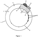
- Fig. 1 is a simplified schematic cross sectional view-of a drum vacuum coater incorporating the present invention.
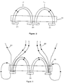
- Fig. 2 is a simplified cross sectional view of a conventional, balanced magnetron sputter device showing the balancing of center and edge magnets.
- Fig. 3 is a simplified cross sectional view of an unbalanced magnetron sputter device showing the lack of balance between the edge magnets and center magnet and the resulting diverging magnetic field above the target.
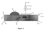
- Fig. 4 is a conceptual drawing of the enhanced broadened plasma generated by the present invention, showing the current paths through the plasma and associated generating system.
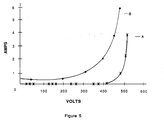
- Fig. 5 is a graph showing a current-voltage characteristic of a magnetron sputter device without an adjacent auxiliary plasma and a current voltage characteristic of a magnetron sputter device operating in one embodiment of the invention.
- Fig. 6 is a simplified schematic view of a preferred embodiment of the invention, showing details of the microwave injection system and electron cyclotron resonance field coils.
- Fig. 7 is a simplified cross sectional view of another embodiment of the present invention, showing a microwave form designed to broaden the auxiliary plasma to better match a linear target plasma.
- Fig. 8 is a table showing the relation between sputtering yield and voltage for a silicon target.
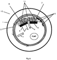
- Fig. 9 is a simplified cross sectional view showing a magnetron sputter device and an adjacent, coupled plasma generating device positioned inside a substrate supporting drum.
- Fig. 10 is a simplified cross sectional view showing magnetron sputter devices and associated adjacent, coupled plasma generating devices inside and outside a substrate supporting drum.
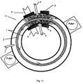
- Fig. 11 is a simplified cross sectional view of a vacuum chamber with cylindrical inner and outer walls both of which house magnetron sputter devices and associated, coupled auxiliary plasma devices for coating from both sides of a rotating substrate bearing drum.
- the process of the present invention is carried out in a vacuum chamber, housing a rotary drum much like the device disclosed in Scobey et al. U.S.Patent 4,851,095, the disclosure of which is hereby incorporated by reference.
- the Scobey et al.-like vacuum drum is modified pursuant to Fig. 1.
- sputtering system 10 comprises housing 1 whose circumference defines a vacuum or low pressure environment.
- housing 1 can be connected to a suitable vacuum pumping system (not shown).
- the pressure within housing 1 is generally in the range of 10 ⁇ 4 to 10 ⁇ 2 Torr.
- Magnetron sputtering device 5 is positioned on the circumference of vacuum housing of chamber 1 located in close proximity to plasma generating device 6.
- an inert sputtering gas such as argon
- a compounding gas such as oxygen
- a compounding gas such as oxygen
- a metal film sputtered from target 5 is deposited. Reaction of this film with the compounding gas begins immediately as the film is deposited in region 9 under the target 5.
- this reaction continues, completing conversion of the film to a dielectric with the desired stoichiometry. Obviously, this sequence can be repeated through rotation of the drum to build a dielectric film of a desired thickness.
- the present invention differs significantly from prior devices of this type in that plasma 11 is spatially continuous over target 5 and plasma generation device 6 and compounding of the film is accomplished continuously in plasma 11. In fact, plasma 11 electrically couples the target and plasma generation device. This is in marked contrast to Scobey et al. which specifically teaches the physical and atmospheric separation of the sputtering target and reaction zones.
- plasma generating device 6 is a microwave device operating at 2.54 gigahertz.
- the plasma 11 is then created by the microwaves and the sputter target operating in concert. If the free electron density of the plasma in region 8 is higher than the critical density for microwaves of 2.54 gigahertz, the frequency ordinarily used, then the plasma is substantially opaque to the microwaves and interdiffusion of the plasma in region 8 with the plasma in region 9 renders the plasma continuous. If the plasma is sufficiently transparent to the microwaves, either through an electron density below the critical density or through operating the microwave in a circularly polarized mode so that the so called whistler mode is operative, then the plasma 11 is rendered continuous through both interdiffusion and absorption of microwaves throughout the plasma.
- the electrical coupling between the target and plasma generator mentioned above can be enhanced, if desired, through design of the magnetic field at the sputter target.
- the magnetic field lines 18 are substantially confined to the region just above the target 19. This is accomplished by making the center magnet 20 twice the width of the outside magnet 21, so that all flux from the outside magnets flows through the center magnet.
- the so-called "unbalanced magnetron” the center magnet 24 is made smaller or replaced by a magnetically permeable material, so that a part of the flux 22 is "pushed" away from the target 23.
- This fringing magnetic field carries part of the plasma away from the target and toward substrate 3 (Fig. 1) and contiguous plasma generating device 6 (Fig. 1).
- operation in this unbalanced mode can have other beneficial effects, as discussed below.
- plasma 11 of Fig. 1 is shown in detail in Fig. 4 as plasma 16.
- the current in plasma 16 is complex, consisting of both ion and electron components.
- the external current through ground 17 to the power supply 15 and through the power supply to sputter target 13, is all electronic.
- the plasma 16 there is a net electron current flow equal to that which passes through the power supply 15.
- the plasma thus acts as a resistive current-carrying element.
- the electron current can go to ground from the plasma at any number of points 12, depending on machine configuration, tooling and other considerations. But in any instance, an electron current is pulled from the plasma as voltage is applied to the target 13.
- the plasma-ground-power supply-target circuit will exhibit a particular voltage at which the target strikes a plasma. Below this voltage, there will be no current. But as soon as the plasma is struck, the power supply begins to pull current from the plasma, the current increasing with increasing target voltage.
- a typical current(I) -voltage(V) curve for a 5 ⁇ x 15 ⁇ silicon target is shown as curve A of Fig. 5 where the microwave device does not contribute to plasma generation. That is, the microwave is not used in generating Curve A.
- the curve shows that below a particular voltage (410 volts in this case) at which the target struck a plasma, there was no current, but as the plasma was struck, the power supply began to pull current from the plasma.
- curve B of Fig. 5 was based upon data generated by initially setting the sputter target voltage to 0 while striking a plasma using only the microwave device. Visually, it was observed that this plasma extended to envelop the sputter target.
- voltage to the sputter target power supply was increased from 0, the power supply began immediately to pull current from the microwave generated plasma. As the voltage was increased further still, so that positive ions accelerated to the target caused secondary electron emission from the target surface, the sputter power supply began to contribute to the plasma.
- I was increased under these conditions, curve B was generated.
- the sputter magnetron and microwave device operate as an integral unit in the generation of a plasma and that changing one influences the operation of the other. This is made clearer still by noting, for example, that as the microwave power increases, the voltage required to maintain a given current through the magnetron sputter supply decreases. This is explained by noting that the increased microwave power lowers the resistance of the plasma.
- the device and process of the present invention are capable of achieving higher sputter rates when compared to prior devices.
- Higher sputter rates follow from the ability of the sputter cathode to draw current from the microwave-induced part of the plasma. This increase in rate is obvious at voltages less than the sputter target striking voltage without the microwave plasma.
- the sputter rate is zero without a plasma being created by the microwave device (Curve A).
- 370 volts there is a significant sputter rate when operating pursuant to the present invention. (Curve B)
- This ability of the present invention to draw ion current from the plasma at low voltages allows sputtering at voltages lower than those of corresponding prior art devices. Since the energy distribution of sputtered atoms shifts toward higher values with increased sputter ion energy, this ability is particularly advantageous in reducing the number of atoms sputtered with higher energies to minimize damage to the growing film.
- the maximum sputter rate is limited by the power that can be applied to the target without damage by debonding from the backplate or warping through over heating.
- the power is increased to the maximum possible.
- the rate of oxide deposition can be much higher than has been therefore achieved.
- use of the present device has resulted in deposited clear SiO2 at over-the-target rates exceeding 180 ⁇ /sec, nearly double those reported in U.S. Patent No. 4,420,385. This is also true for other materials as well, as the following discussion reveals.
- the present invention increases the oxygen, or other reactive gas, that can be introduced into the vacuum chamber before the target surface becomes completely covered by an oxide layer; that is, before the target is "poisoned.” This results from the ability of the enhanced plasma to create active oxygen species which readily react with the growing film.
- This film is in effect a second pump for the reactive gas, the vacuum system pump being the first.
- the pumping speed of the second pump is greater as the oxygen, or other reactive gas, is made more reactive.
- the device operates with 2 to 3 KW of microwave power distributed over a plasma 8 to 10 inches in length. This is in marked contrast to the few hundred watts over 20-25 inches cited in U.S. Patent No. 4,420,385, for example.
- This high input power into the broadened enhanced plasma of the present invention is especially effective in exciting the reactive gas and therefore in increasing the pumping speed of the growing film.
- the enhanced plasma device of the present invention often provides complete oxidizing, or nitriding, etc, at reactive gas flows well below the target poisoning level. This mode of operation is often convenient when very stable operation is desired; that is, when operation away from the poisoning knee of the system curve is desired.
- the present invention is capable of striking a plasma at much lower pressures than those normally used in magnetron sputtering.
- a DC magnetron requires pressure higher than 10 ⁇ 3 Torr
- the present invention is capable of striking a plasma at pressures well below 10 ⁇ 4 Torr.
- the present invention is capable of drawing sputtering current at pressures for which the mean collision path is greater than 50 cm. This can be advantageous when line-of-sight deposition is required; that is, when scattering of the sputtered atoms is detrimental to the growing film. This can, for example, prevent high angles of incidence deposition which can lead to porous or stressed films.
- Low pressure operation is achieved by using a microwave generator as the plasma enhancing device.
- the microwaves into the system through 6 reflect from the metal drum 2, causing an intense standing wave in the region above the drum 2, the region in which the plasma is desired.
- the drum 2 becomes part of a high Q microwave cavity in which intense fields capable of plasma generations at pressures down to approximately 5 x 10 ⁇ 4 Torr can be struck and maintained.
- ECR electron cyclotron resonance
- the magnetic field B for ECR operation can be generated in any number of ways.
- a current carrying coil can be wrapped around the microwave waveguide as it enters the vacuum chamber.
- a permanent magnet in the region of the microwave windows on the chamber. When this done, an ECR induced plasma will strike in those regions around the magnet where the magnetic field is 875 gauss.
- the present invention is also capable of depositing some non-oxide dieletrics more effectively than is possible using prior art.
- titanium nitride TiN
- TiN titanium nitride
- titanium dioxide is a clear coating often used in optical filters. Titanium metal reacts readily with oxygen but is essentially nonreactive with nitrogen. To obtain a good TiN film one thus needs a plasma to excite the nitrogen and render it more reactive, and one needs to exclude oxygen from the deposition system to the maximum degree possible.
- a titanium target is employed and nitrogen gas bled into the system after an initial pumpdown.
- the pumpdown removes oxygen from the system, with temperature and vacuum chamber history being important variables in determining the time required. For example, if the chamber has a thick, porous coating on its walls from previous runs, then a long time may be required for water vapor to be desorbed from the walls. As such, there will always be some residual oxygen in the system and this oxygen will compete with nitrogen in reacting with the sputtered Ti film. Because oxygen is so much more reactive than nitrogen, even a small amount can be detrimental.
- substrates are placed upon the drum which is, for example, rotated at 30 rpm.
- the microwave source is positioned on the counterclockwise side of the magnetron sputter target as shown in Fig. 1
- the Ti metal is sputtered only in the vicinity of the magnetron whereupon the substrates pass directly into the zone dominated by the microwave device.
- exposure to background oxygen is minimal, since the reaction started at the site of the target is completed at the site of the microwave device and no free Ti is available for reaction after passing through the microwave input zone.
- the sputter target is configured in the unbalanced mode as briefly described earlier in reference to Fig. 3. It is well known that the quality of a thin film can be influenced through bombardment of the film by energetic atoms during deposition. The energy of these atoms is preferably great enough to move atoms around on the growing film and small enough to avoid significant sputtering of the film. To restate, it is desirable to increase the mobility of the atoms while avoiding their resputtering. This is best accomplished when the energy of the bombarding species is between about ten and one hundred electron volts. The unbalanced magnetron of Fig. 3 provides ions at the substrate in this energy range.
- the unbalanced magnetron can be used as the sputter target in the present invention with plasma enhancement and broadening being provided by, for example, the microwave system discussed above as part of a preferred embodiment. It can also be used as the auxiliary plasma generator in conjunction with a contiguous sputter target which itself may or may not be unbalanced. In this mode the unbalanced auxiliary would operate in the poisoned mode to provide an intense plasma while sputtering at a low rate and the sputter target per se would operate in the unpoisoned mode to provide the desired metal atoms at a high rate.
- the auxiliary target was of the same material as the main sputter target, so that any material sputtered from it would simply add to the growing film and not contaminate it. This can sometimes be inconvenient and/or less efficient than desired in enhancing the plasma, the latter when insufficient power is applied without cleaning the auxiliary target of it's poisoned surface layer.
- auxiliary target of another material that has a low sputter yield or the incorporation of small amounts of which into the growing film is of no practical consequence.
- a poisoned Si target as an auxiliary and an unpoisoned aluminum target as the main. Since even in the unpoisoned state silicon has a sputtering yield less than one half that of the aluminum, very little silicon would be incorporated into the film, and this as SiO2. For most applications this small amount of SiO2 in Al2O3 would be insignificant.
- a preferred embodiment of the present invention utilizes a microwave generator as the plasma enhancement device 6 of Fig. 1.
- a microwave generator as the plasma enhancement device 6 of Fig. 1.
- One embodiment is shown in Fig. 6 as a side view of the vacuum chamber 25 and rotable drum 26 on which substrates 27 are mounted.
- a microwave transparent window 30 made of, for example, fused quartz, is mounted on the wall of the chamber.
- a waveguide 28 directs microwaves through the window 30 enhancing the plasma 31.
- the microwave frequency is 2.54 GHz and the waveguide and window are suitably sized for this frequency.
- the waveguide is WR284, which is rectangular and measures 3 inches x 1.5 inches.
- the window is circular and approximately 3 inches in diameter.
- the microwave power supply is capable of generating 3 KW of microwave power. This is tuned to the plasma 30 using a stub tuner 29 in the waveguide 28.
- the sputter target (not shown in Fig. 6) in one embodiment is 5 ⁇ x 15 ⁇ and is positioned on the outside circumference of the vacuum chamber 25 adjacent to the microwave window 30.
- the separation of the target and window is typically less than about ten inches, allowing the plasma 31 to diffuse readily between the microwave window 30 region and the target region so that the advantages of the invention as discussed previously can be realized.
- a rainbow-like coating is observed at the microwave window. This is a metal oxide coating formed by metal atoms from the sputter target and oxygen, and it evidences a coupling of the plasmas generated at the target and the microwave generating device as well as a significant excitation of metal and oxygen atoms in the entire region of the continuous plasma..
- a magnetic field 32 is generated in the plasma 31 by a current carrying coil 33 wrapped around the waveguide 28.
- the ampere turns in this coil are sufficient to create a field strength of 875 G over some surface in the plasma 31, thereby causing ECR operation at that surface. It has been found that 400 amperes through 75 turns is sufficient to accomplish this.
- the magnetic field 32 can also act as a magnetic mirror to keep the hot plasma 31 away from the window 30, thereby allowing higher power without damaging the window or vacuum seals.
- the magnetic mirror effect occurs at field levels below those needed for ECR operation and the invention can be so operated if desired.
- the invention can also utilize a microwave horn as shown in Fig. 7.
- microwaves are injected through a WR284 waveguide 35 into a microwave horn 36.
- the length of this horn along the drum is approximately 15 inches when used with a 25 ⁇ target.
- the microwave window 37 mounted in the chamber wall 38 is rectangular, measuring fifteen inches by 3 inches. In this arrangement a long plasma 39 is created allowing activation of film on substrates 40 and coupled operation with the sputter target (not shown).
- Drum 2 was first rotated counterclockwise to produce Sample A and the direction of rotation reversed to a clockwise direction to create Sample B.
- the resulting films were partially transparent but Sample B more so than Sample A.
- the conductivity of Sample A was measured at 10 ohms/square while that of Sample B was 25 ohms/square. These measurements clearly indicate that Sample A was better nitrided than Sample B. Stated differently, Sample B was partially oxidized by its longer exposure to the oxygen background.
- the device as depicted in Fig. 1 was configured with a silicon target and a microwave plasma generator with deposition conditions listed in Table 2. Under these conditions a clear, fully oxidized film of SiO2 was obtained at an over the target deposition rate of 180 ⁇ /sec. This is much greater than the 100 ⁇ /sec achieved by U.S. Patent No. 4,851,095 using separate sputter and deposition zones.
- the device as depicted in Fig. 1 was configured with a tantalum metal target and the deposition conditions listed in Table 3 were established. Under these conditions a clear film of Ta2O5 was deposited at an over the target rate of 120 ⁇ /sec which was obtained without baking the part after deposition; a process commonly used to complete oxidation of thin films as taught in U.S. Patent No. 4,851,051.
- deposition rates can be increased if a post deposition bake can be used to complete reaction of the film; that is, to remove residual absorption from the film.
- a post deposition bake can be used to complete reaction of the film; that is, to remove residual absorption from the film.
- the present invention To deposit Ta2O5 the device was configured as depicted in Fig. 1 and the deposition conditions listed in Table 4 were established and a one micron film was deposited at a rate of 210 ⁇ /sec. The film was absorbing upon removal from the coating chamber but cleared after baking for 30 minutes at 600° C. This is in contrast to the 150 ⁇ /sec achieved in U.S. Patent 4,851,095.
- a film of AIN the device as depicted in Fig 1 was fitted with an aluminum target and the deposition conditions of Table 5 were established. Under these conditions a hard, clear film of AIN of 3.5 microns thickness was produced at an over the target deposition rate of 60 ⁇ /sec. This film was very suitable as a transparent wear resistant coating.
- the present invention has a wide variety of applications, including multilayer interference filters, opaque wear resistant coatings, transparent wear resistant coatings, layered ultrathin coherent structures (LUCS), transparent conductive coatings, and others. Some of these applications are briefly described below.
- the invention was employed to deposit a conductive tin oxide using a tin target and a microwave generated auxiliary plasma.
- the resulting coating was clear with conductivity 10 ⁇ 4 ohm-cm.
- the invention is also suitable for depositing filters on lamps.
- a filter transmitting in the visible and reflecting in the infrared, out to about 2 microns has been used as an energy device for incandescent lamps, especially tungsten halogen lamps.
- the reflected infrared energy maintains the filament temperature at a given level with less electrical input, thereby yielding visible light at lower cost.
- filters and lamps are well known. They are produced in volume by The General Electric Co., and are described in U.S. Patent 4,851,095.
- These IR reflecting filters on lamps can be deposited using the present invention by providing tooling to rotate the lamps as they pass through the sputtering - activating plasma.
- Nb2O5/SiO2 and TiO2/SiO2 have been used as material pairs to make the filters.
- MR 16's form an example of the latter. These are half paraboloids measuring 16 eighths of an inch across. They are used, for example, in overhead projectors.
- the present invention is particularly suitable for coating these MR 16's. It's high deposition rates allow very stable oxides to be deposited economically in this commodity product.
- a structure consisting of 6 b layers of SiO2 interleaved with 10 ⁇ layers of TiO2 to a total film thickness of 1 micron is readily made at a drum rotation rate of 10rpm, and three and five kilowatts of power respectively to the silicon and titanium target.
- Fig. 9 shows an auxiliary plasma generating device 6 coupled to a sputter target 5 on the inside of a rotating, substrate bearing drum 2.
- Fig. 10 shows coupled auxiliary devices 6 and sputter targets 5 on both the inside and outside of a substrate bearing drum 2.
- Fig. 11 shows a novel "donut" configuration in which the vacuum chamber 1 has cylindrical inner and outer vacuum walls 1 with coupled auxiliary devices 6 and sputter targets 5 mounted in the walls 1. It is obvious that such a configuration allows coating of substrates facing either in or out on the drum and therefore effectively doubles the load size.
Landscapes
- Chemical & Material Sciences (AREA)
- Engineering & Computer Science (AREA)
- Organic Chemistry (AREA)
- Materials Engineering (AREA)
- Mechanical Engineering (AREA)
- Metallurgy (AREA)
- Chemical Kinetics & Catalysis (AREA)
- Physics & Mathematics (AREA)
- Plasma & Fusion (AREA)
- Analytical Chemistry (AREA)
- Thermal Sciences (AREA)
- Physical Vapour Deposition (AREA)
- Glass Compositions (AREA)
- Encapsulation Of And Coatings For Semiconductor Or Solid State Devices (AREA)
- Electrodes Of Semiconductors (AREA)
Applications Claiming Priority (2)
| Application Number | Priority Date | Filing Date | Title |
|---|---|---|---|
| US70903591A | 1991-05-31 | 1991-05-31 | |
| US709035 | 1991-05-31 |
Publications (3)
| Publication Number | Publication Date |
|---|---|
| EP0516436A2 true EP0516436A2 (fr) | 1992-12-02 |
| EP0516436A3 EP0516436A3 (en) | 1993-03-31 |
| EP0516436B1 EP0516436B1 (fr) | 1997-01-15 |
Family
ID=24848218
Family Applications (1)
| Application Number | Title | Priority Date | Filing Date |
|---|---|---|---|
| EP92304870A Expired - Lifetime EP0516436B1 (fr) | 1991-05-31 | 1992-05-28 | Dispositif de pulvérisation |
Country Status (4)
| Country | Link |
|---|---|
| EP (1) | EP0516436B1 (fr) |
| JP (1) | JP3420594B2 (fr) |
| AT (1) | ATE147890T1 (fr) |
| DE (1) | DE69216685T2 (fr) |
Cited By (16)
| Publication number | Priority date | Publication date | Assignee | Title |
|---|---|---|---|---|
| DE4305748A1 (de) * | 1993-02-25 | 1994-09-01 | Leybold Ag | Vorrichtung zum Beschichten und/oder Ätzen von Substraten in einer Vakuumkammer |
| EP0707663A4 (fr) * | 1993-06-17 | 1998-01-14 | Deposition Sciences Inc | Dispositif de pulverisation |
| DE19722056A1 (de) * | 1997-05-27 | 1998-12-03 | Roland Dr Gesche | Verfahren und Anordnung zum Herstellen dünner Schichten mittels Niederdruck-Gasentladung in einer Hohlkathode |
| WO1999053526A1 (fr) * | 1998-04-08 | 1999-10-21 | Koninklijke Philips Electronics N.V. | Lampe electrique a filtre d'interface optique |
| EP0823944A4 (fr) * | 1995-04-25 | 2000-09-20 | Deposition Sciences Inc | Dispositif de pulverisation |
| EP0824604A4 (fr) * | 1995-05-09 | 2001-06-13 | Deposition Sciences Inc | Appareil permettant de reduire le risque de formation d'arc en cours de pulverisation cathodique |
| US6472022B1 (en) | 1999-04-09 | 2002-10-29 | Matsushita Electric Industrial Co., Ltd. | Method for forming thin film, spheroid coated with thin film, light bulb using the spheroid and equipment for film formation |
| GB2379224A (en) * | 2001-08-13 | 2003-03-05 | Hon Hai Prec Industry Company | Deposition system design for depositing DWDM filter. |
| WO2004026787A1 (fr) * | 2002-09-14 | 2004-04-01 | Schott Ag | Procede de realisation de couches et de systemes de couches, et substrat recouvert |
| EP0809719A4 (fr) * | 1995-02-13 | 2006-07-26 | Deposition Sciences Inc | Appareil et procede permettant d'obtenir un chemin de retour de courant fiable pour des techniques de pulverisation cathodique |
| EP1680527A4 (fr) * | 2003-10-07 | 2008-10-22 | Deposition Sciences Inc | Appareil et procede pour le depot haute vitesse de dioxyde de titane de rutile |
| WO2009027905A2 (fr) | 2007-08-30 | 2009-03-05 | Koninklijke Philips Electronics N.V. | Système de pulvérisation cathodique |
| CN101027423B (zh) * | 2004-08-30 | 2010-12-01 | 株式会社爱发科 | 成膜装置 |
| EP3396016A4 (fr) * | 2015-12-24 | 2019-08-28 | Konica Minolta, Inc. | Appareil de formation de film et procédé de formation de film |
| US11814718B2 (en) | 2015-03-31 | 2023-11-14 | Bühler Alzenau Gmbh | Method for producing coated substrates |
| WO2024113239A1 (fr) * | 2022-11-30 | 2024-06-06 | 江阴纳力新材料科技有限公司 | Mécanisme de rouleau de gravure et module de revêtement |
Families Citing this family (5)
| Publication number | Priority date | Publication date | Assignee | Title |
|---|---|---|---|---|
| EP1554412B1 (fr) * | 2002-09-19 | 2013-08-14 | General Plasma, Inc. | Appareil de dépôt chimique en phase vapeur assisté par plasma |
| GB0505517D0 (en) * | 2005-03-17 | 2005-04-27 | Dupont Teijin Films Us Ltd | Coated polymeric substrates |
| JP2007092095A (ja) * | 2005-09-27 | 2007-04-12 | Shincron:Kk | 薄膜形成方法及び薄膜形成装置 |
| EP1999776A1 (fr) * | 2006-03-28 | 2008-12-10 | NV Bekaert SA | Appareil pour revêtement |
| GB201603233D0 (en) * | 2016-02-24 | 2016-04-06 | Gencoa Ltd | Ionisation enhancement device |
Family Cites Families (6)
| Publication number | Priority date | Publication date | Assignee | Title |
|---|---|---|---|---|
| DE2307649B2 (de) * | 1973-02-16 | 1980-07-31 | Robert Bosch Gmbh, 7000 Stuttgart | Anordnung zum Aufstäuben verschiedener Materialien auf einem Substrat |
| US4026787A (en) * | 1974-01-25 | 1977-05-31 | Coulter Information Systems, Inc. | Thin film deposition apparatus using segmented target means |
| EP0103461B1 (fr) * | 1982-09-10 | 1988-11-17 | Nippon Telegraph And Telephone Corporation | Appareil et procédé de dépôt à plasma |
| JPH0627323B2 (ja) * | 1983-12-26 | 1994-04-13 | 株式会社日立製作所 | スパツタリング方法及びその装置 |
| EP0173164B1 (fr) * | 1984-08-31 | 1988-11-09 | Hitachi, Ltd. | Vaporisation à l'aide de micro-ondes |
| US4892633A (en) * | 1988-11-14 | 1990-01-09 | Vac-Tec Systems, Inc. | Magnetron sputtering cathode |
-
1992
- 1992-05-28 AT AT92304870T patent/ATE147890T1/de not_active IP Right Cessation
- 1992-05-28 DE DE69216685T patent/DE69216685T2/de not_active Expired - Lifetime
- 1992-05-28 EP EP92304870A patent/EP0516436B1/fr not_active Expired - Lifetime
- 1992-05-29 JP JP13928292A patent/JP3420594B2/ja not_active Expired - Lifetime
Cited By (23)
| Publication number | Priority date | Publication date | Assignee | Title |
|---|---|---|---|---|
| DE4305748A1 (de) * | 1993-02-25 | 1994-09-01 | Leybold Ag | Vorrichtung zum Beschichten und/oder Ätzen von Substraten in einer Vakuumkammer |
| US5429705A (en) * | 1993-02-25 | 1995-07-04 | Leybold Aktiengesellschaft | Apparatus for coating and/or etching substrates in a vacuum chamber |
| EP0707663A4 (fr) * | 1993-06-17 | 1998-01-14 | Deposition Sciences Inc | Dispositif de pulverisation |
| EP0809719A4 (fr) * | 1995-02-13 | 2006-07-26 | Deposition Sciences Inc | Appareil et procede permettant d'obtenir un chemin de retour de courant fiable pour des techniques de pulverisation cathodique |
| EP0823944A4 (fr) * | 1995-04-25 | 2000-09-20 | Deposition Sciences Inc | Dispositif de pulverisation |
| EP0824604A4 (fr) * | 1995-05-09 | 2001-06-13 | Deposition Sciences Inc | Appareil permettant de reduire le risque de formation d'arc en cours de pulverisation cathodique |
| DE19722056A1 (de) * | 1997-05-27 | 1998-12-03 | Roland Dr Gesche | Verfahren und Anordnung zum Herstellen dünner Schichten mittels Niederdruck-Gasentladung in einer Hohlkathode |
| WO1999053526A1 (fr) * | 1998-04-08 | 1999-10-21 | Koninklijke Philips Electronics N.V. | Lampe electrique a filtre d'interface optique |
| US6049169A (en) * | 1998-04-08 | 2000-04-11 | Philips Electronics North America Corp. | Electric lamp having optical interference filter of alternating layers of SiO2 and Nb2 O5 --Ta2 O5 |
| US6635330B2 (en) | 1999-04-09 | 2003-10-21 | Matsushita Electric Industrial Co., Ltd. | Method for forming thin film, spheroid coated with thin film, light bulb using the spheroid and equipment for film formation |
| US6726816B2 (en) | 1999-04-09 | 2004-04-27 | Matsushita Electric Industrial Co., Ltd. | Method for forming thin film, spheroid coated with thin film, light bulb using the spheroid and equipment for film formation |
| US6472022B1 (en) | 1999-04-09 | 2002-10-29 | Matsushita Electric Industrial Co., Ltd. | Method for forming thin film, spheroid coated with thin film, light bulb using the spheroid and equipment for film formation |
| GB2379224A (en) * | 2001-08-13 | 2003-03-05 | Hon Hai Prec Industry Company | Deposition system design for depositing DWDM filter. |
| WO2004026787A1 (fr) * | 2002-09-14 | 2004-04-01 | Schott Ag | Procede de realisation de couches et de systemes de couches, et substrat recouvert |
| KR100885083B1 (ko) * | 2002-09-14 | 2009-02-25 | 쇼오트 아게 | 층 및 층 시스템을 제조하는 방법과 코팅 기판 |
| US7641773B2 (en) | 2002-09-14 | 2010-01-05 | Schott Ag | Process for producing layers and layer systems, and coated substrate |
| EP1680527A4 (fr) * | 2003-10-07 | 2008-10-22 | Deposition Sciences Inc | Appareil et procede pour le depot haute vitesse de dioxyde de titane de rutile |
| CN101027423B (zh) * | 2004-08-30 | 2010-12-01 | 株式会社爱发科 | 成膜装置 |
| WO2009027905A2 (fr) | 2007-08-30 | 2009-03-05 | Koninklijke Philips Electronics N.V. | Système de pulvérisation cathodique |
| CN101796213B (zh) * | 2007-08-30 | 2012-07-11 | 皇家飞利浦电子股份有限公司 | 溅射系统 |
| US11814718B2 (en) | 2015-03-31 | 2023-11-14 | Bühler Alzenau Gmbh | Method for producing coated substrates |
| EP3396016A4 (fr) * | 2015-12-24 | 2019-08-28 | Konica Minolta, Inc. | Appareil de formation de film et procédé de formation de film |
| WO2024113239A1 (fr) * | 2022-11-30 | 2024-06-06 | 江阴纳力新材料科技有限公司 | Mécanisme de rouleau de gravure et module de revêtement |
Also Published As
| Publication number | Publication date |
|---|---|
| DE69216685T2 (de) | 1997-05-28 |
| JPH05156436A (ja) | 1993-06-22 |
| EP0516436B1 (fr) | 1997-01-15 |
| EP0516436A3 (en) | 1993-03-31 |
| ATE147890T1 (de) | 1997-02-15 |
| JP3420594B2 (ja) | 2003-06-23 |
| DE69216685D1 (de) | 1997-02-27 |
Similar Documents
| Publication | Publication Date | Title |
|---|---|---|
| EP0516436B1 (fr) | Dispositif de pulvérisation | |
| EP0945523B1 (fr) | Procédé pour obtenir un film mince et appareillage pour la mise en oeuvre de ce procédé | |
| EP0908531B1 (fr) | Appareillage et procédé pour déposer une couche mince d'un composé | |
| JPH03211275A (ja) | マグネトロンスパッタリング装置及び方法 | |
| JP3774353B2 (ja) | 金属化合物薄膜の形成方法およびその形成装置 | |
| WO1996034125A1 (fr) | Dispositif de pulverisation | |
| WO1995000677A1 (fr) | Dispositif de pulverisation | |
| AU692332B2 (en) | Process and apparatus for forming thin films of metallic compounds | |
| JP3124288B2 (ja) | マイクロ波により生成され、ガス支援下のプラズマ中での基板処理装置 | |
| JPH11256327A (ja) | 金属化合物薄膜の形成方法および成膜装置 | |
| EP0691419A1 (fr) | Procédé et dispositif pour la formation de films optiques multicouches | |
| Lehan et al. | High‐rate aluminum oxide deposition by MetaModeTM reactive sputtering | |
| JPH11279758A (ja) | 金属化合物薄膜の形成方法および成膜装置 | |
| Safi | A novel reactive magnetron sputtering technique for producing insulating oxides of metal alloys and other compound thin films | |
| McNeil et al. | Ion beam deposition | |
| EP1680527B1 (fr) | Appareil et procede pour le depot haute vitesse de dioxyde de titane de rutile | |
| JP3738154B2 (ja) | 複合金属化合物の薄膜形成方法及びその薄膜形成装置 | |
| Futagami et al. | Characterization of RF-enhanced DC sputtering to deposit tin-doped indium oxide thin films | |
| Martin Mišina et al. | Ion assisted deposition of crystalline TiNi thin films by electron cyclotron resonance plasma enhanced sputtering | |
| JPH0831417B2 (ja) | プラズマ加工堆積装置 | |
| Cook et al. | Characterization of a radio‐frequency discharge used for downstream plasma oxidation of Si | |
| Shuhua et al. | Ions bombardment in thin films and surface processing | |
| Vašina¹ et al. | PHYSICAL VAPOUR DEPOSITION: CONCEPTS |
Legal Events
| Date | Code | Title | Description |
|---|---|---|---|
| PUAI | Public reference made under article 153(3) epc to a published international application that has entered the european phase |
Free format text: ORIGINAL CODE: 0009012 |
|
| AK | Designated contracting states |
Kind code of ref document: A2 Designated state(s): AT BE CH DE ES FR GB GR IT LI LU NL SE |
|
| PUAL | Search report despatched |
Free format text: ORIGINAL CODE: 0009013 |
|
| AK | Designated contracting states |
Kind code of ref document: A3 Designated state(s): AT BE CH DE ES FR GB GR IT LI LU NL SE |
|
| 17P | Request for examination filed |
Effective date: 19930928 |
|
| 17Q | First examination report despatched |
Effective date: 19941108 |
|
| GRAG | Despatch of communication of intention to grant |
Free format text: ORIGINAL CODE: EPIDOS AGRA |
|
| GRAH | Despatch of communication of intention to grant a patent |
Free format text: ORIGINAL CODE: EPIDOS IGRA |
|
| GRAH | Despatch of communication of intention to grant a patent |
Free format text: ORIGINAL CODE: EPIDOS IGRA |
|
| GRAA | (expected) grant |
Free format text: ORIGINAL CODE: 0009210 |
|
| AK | Designated contracting states |
Kind code of ref document: B1 Designated state(s): AT BE CH DE ES FR GB GR IT LI LU NL SE |
|
| PG25 | Lapsed in a contracting state [announced via postgrant information from national office to epo] |
Ref country code: GR Free format text: LAPSE BECAUSE OF FAILURE TO SUBMIT A TRANSLATION OF THE DESCRIPTION OR TO PAY THE FEE WITHIN THE PRESCRIBED TIME-LIMIT Effective date: 19970115 Ref country code: ES Free format text: THE PATENT HAS BEEN ANNULLED BY A DECISION OF A NATIONAL AUTHORITY Effective date: 19970115 |
|
| REF | Corresponds to: |
Ref document number: 147890 Country of ref document: AT Date of ref document: 19970215 Kind code of ref document: T |
|
| REG | Reference to a national code |
Ref country code: CH Ref legal event code: EP |
|
| REG | Reference to a national code |
Ref country code: CH Ref legal event code: NV Representative=s name: BOVARD AG PATENTANWAELTE |
|
| ET | Fr: translation filed | ||
| ITF | It: translation for a ep patent filed | ||
| REF | Corresponds to: |
Ref document number: 69216685 Country of ref document: DE Date of ref document: 19970227 |
|
| PG25 | Lapsed in a contracting state [announced via postgrant information from national office to epo] |
Ref country code: SE Effective date: 19970415 |
|
| PG25 | Lapsed in a contracting state [announced via postgrant information from national office to epo] |
Ref country code: LU Free format text: LAPSE BECAUSE OF NON-PAYMENT OF DUE FEES Effective date: 19970531 |
|
| PLBQ | Unpublished change to opponent data |
Free format text: ORIGINAL CODE: EPIDOS OPPO |
|
| PLBI | Opposition filed |
Free format text: ORIGINAL CODE: 0009260 |
|
| PLBF | Reply of patent proprietor to notice(s) of opposition |
Free format text: ORIGINAL CODE: EPIDOS OBSO |
|
| 26 | Opposition filed |
Opponent name: OPTICAL COATING LABORATORY INC. Effective date: 19971015 |
|
| NLR1 | Nl: opposition has been filed with the epo |
Opponent name: OPTICAL COATING LABORATORY INC. |
|
| PLBF | Reply of patent proprietor to notice(s) of opposition |
Free format text: ORIGINAL CODE: EPIDOS OBSO |
|
| PLBF | Reply of patent proprietor to notice(s) of opposition |
Free format text: ORIGINAL CODE: EPIDOS OBSO |
|
| PLBQ | Unpublished change to opponent data |
Free format text: ORIGINAL CODE: EPIDOS OPPO |
|
| PLAB | Opposition data, opponent's data or that of the opponent's representative modified |
Free format text: ORIGINAL CODE: 0009299OPPO |
|
| R26 | Opposition filed (corrected) |
Opponent name: OPTICAL COATING LABORATORY INC. Effective date: 19971015 |
|
| NLR1 | Nl: opposition has been filed with the epo |
Opponent name: OPTICAL COATING LABORATORY INC. |
|
| PLBO | Opposition rejected |
Free format text: ORIGINAL CODE: EPIDOS REJO |
|
| APAC | Appeal dossier modified |
Free format text: ORIGINAL CODE: EPIDOS NOAPO |
|
| APAE | Appeal reference modified |
Free format text: ORIGINAL CODE: EPIDOS REFNO |
|
| APAC | Appeal dossier modified |
Free format text: ORIGINAL CODE: EPIDOS NOAPO |
|
| PGFP | Annual fee paid to national office [announced via postgrant information from national office to epo] |
Ref country code: AT Payment date: 20010514 Year of fee payment: 10 |
|
| PGFP | Annual fee paid to national office [announced via postgrant information from national office to epo] |
Ref country code: FR Payment date: 20010518 Year of fee payment: 10 |
|
| PGFP | Annual fee paid to national office [announced via postgrant information from national office to epo] |
Ref country code: CH Payment date: 20010529 Year of fee payment: 10 |
|
| PGFP | Annual fee paid to national office [announced via postgrant information from national office to epo] |
Ref country code: NL Payment date: 20010531 Year of fee payment: 10 |
|
| PGFP | Annual fee paid to national office [announced via postgrant information from national office to epo] |
Ref country code: BE Payment date: 20010717 Year of fee payment: 10 |
|
| REG | Reference to a national code |
Ref country code: GB Ref legal event code: IF02 |
|
| PG25 | Lapsed in a contracting state [announced via postgrant information from national office to epo] |
Ref country code: AT Free format text: LAPSE BECAUSE OF NON-PAYMENT OF DUE FEES Effective date: 20020528 |
|
| PG25 | Lapsed in a contracting state [announced via postgrant information from national office to epo] |
Ref country code: LI Free format text: LAPSE BECAUSE OF NON-PAYMENT OF DUE FEES Effective date: 20020531 Ref country code: CH Free format text: LAPSE BECAUSE OF NON-PAYMENT OF DUE FEES Effective date: 20020531 Ref country code: BE Free format text: LAPSE BECAUSE OF NON-PAYMENT OF DUE FEES Effective date: 20020531 |
|
| PG25 | Lapsed in a contracting state [announced via postgrant information from national office to epo] |
Ref country code: NL Free format text: LAPSE BECAUSE OF NON-PAYMENT OF DUE FEES Effective date: 20021201 |
|
| GBPC | Gb: european patent ceased through non-payment of renewal fee |
Effective date: 20020528 |
|
| REG | Reference to a national code |
Ref country code: CH Ref legal event code: PL |
|
| PG25 | Lapsed in a contracting state [announced via postgrant information from national office to epo] |
Ref country code: FR Free format text: LAPSE BECAUSE OF NON-PAYMENT OF DUE FEES Effective date: 20030131 |
|
| NLV4 | Nl: lapsed or anulled due to non-payment of the annual fee |
Effective date: 20021201 |
|
| REG | Reference to a national code |
Ref country code: FR Ref legal event code: ST |
|
| REG | Reference to a national code |
Ref country code: FR Ref legal event code: RN |
|
| REG | Reference to a national code |
Ref country code: FR Ref legal event code: D5 |
|
| APBU | Appeal procedure closed |
Free format text: ORIGINAL CODE: EPIDOSNNOA9O |
|
| REG | Reference to a national code |
Ref country code: GB Ref legal event code: 728V |
|
| APBW | Interlocutory revision of appeal recorded |
Free format text: ORIGINAL CODE: EPIDOSNIRAPO |
|
| PLBN | Opposition rejected |
Free format text: ORIGINAL CODE: 0009273 |
|
| STAA | Information on the status of an ep patent application or granted ep patent |
Free format text: STATUS: OPPOSITION REJECTED |
|
| 27O | Opposition rejected |
Effective date: 20031210 |
|
| REG | Reference to a national code |
Ref country code: GB Ref legal event code: 728Y |
|
| PG25 | Lapsed in a contracting state [announced via postgrant information from national office to epo] |
Ref country code: IT Free format text: LAPSE BECAUSE OF NON-PAYMENT OF DUE FEES;WARNING: LAPSES OF ITALIAN PATENTS WITH EFFECTIVE DATE BEFORE 2007 MAY HAVE OCCURRED AT ANY TIME BEFORE 2007. THE CORRECT EFFECTIVE DATE MAY BE DIFFERENT FROM THE ONE RECORDED. Effective date: 20050528 |
|
| APAH | Appeal reference modified |
Free format text: ORIGINAL CODE: EPIDOSCREFNO |
|
| PGFP | Annual fee paid to national office [announced via postgrant information from national office to epo] |
Ref country code: GB Payment date: 20110406 Year of fee payment: 20 |
|
| PGFP | Annual fee paid to national office [announced via postgrant information from national office to epo] |
Ref country code: DE Payment date: 20110629 Year of fee payment: 20 |
|
| REG | Reference to a national code |
Ref country code: DE Ref legal event code: R071 Ref document number: 69216685 Country of ref document: DE |
|
| REG | Reference to a national code |
Ref country code: DE Ref legal event code: R071 Ref document number: 69216685 Country of ref document: DE |
|
| REG | Reference to a national code |
Ref country code: GB Ref legal event code: PE20 Expiry date: 20120527 |
|
| PG25 | Lapsed in a contracting state [announced via postgrant information from national office to epo] |
Ref country code: DE Free format text: LAPSE BECAUSE OF EXPIRATION OF PROTECTION Effective date: 20120530 |
|
| PG25 | Lapsed in a contracting state [announced via postgrant information from national office to epo] |
Ref country code: GB Free format text: LAPSE BECAUSE OF EXPIRATION OF PROTECTION Effective date: 20120527 |