EP0517440A2 - Article ou système comprenant un dispositif optique à base de silicium - Google Patents
Article ou système comprenant un dispositif optique à base de silicium Download PDFInfo
- Publication number
- EP0517440A2 EP0517440A2 EP92304896A EP92304896A EP0517440A2 EP 0517440 A2 EP0517440 A2 EP 0517440A2 EP 92304896 A EP92304896 A EP 92304896A EP 92304896 A EP92304896 A EP 92304896A EP 0517440 A2 EP0517440 A2 EP 0517440A2
- Authority
- EP
- European Patent Office
- Prior art keywords
- article
- waveguide means
- luminescence
- waveguide
- core region
- Prior art date
- Legal status (The legal status is an assumption and is not a legal conclusion. Google has not performed a legal analysis and makes no representation as to the accuracy of the status listed.)
- Granted
Links
Images

Classifications
-
- H—ELECTRICITY
- H10—SEMICONDUCTOR DEVICES; ELECTRIC SOLID-STATE DEVICES NOT OTHERWISE PROVIDED FOR
- H10H—INORGANIC LIGHT-EMITTING SEMICONDUCTOR DEVICES HAVING POTENTIAL BARRIERS
- H10H20/00—Individual inorganic light-emitting semiconductor devices having potential barriers, e.g. light-emitting diodes [LED]
- H10H20/80—Constructional details
- H10H20/81—Bodies
- H10H20/822—Materials of the light-emitting regions
- H10H20/826—Materials of the light-emitting regions comprising only Group IV materials
- H10H20/8262—Materials of the light-emitting regions comprising only Group IV materials characterised by the dopants
-
- H—ELECTRICITY
- H01—ELECTRIC ELEMENTS
- H01S—DEVICES USING THE PROCESS OF LIGHT AMPLIFICATION BY STIMULATED EMISSION OF RADIATION [LASER] TO AMPLIFY OR GENERATE LIGHT; DEVICES USING STIMULATED EMISSION OF ELECTROMAGNETIC RADIATION IN WAVE RANGES OTHER THAN OPTICAL
- H01S5/00—Semiconductor lasers
- H01S5/50—Amplifier structures not provided for in groups H01S5/02 - H01S5/30
-
- H—ELECTRICITY
- H01—ELECTRIC ELEMENTS
- H01S—DEVICES USING THE PROCESS OF LIGHT AMPLIFICATION BY STIMULATED EMISSION OF RADIATION [LASER] TO AMPLIFY OR GENERATE LIGHT; DEVICES USING STIMULATED EMISSION OF ELECTROMAGNETIC RADIATION IN WAVE RANGES OTHER THAN OPTICAL
- H01S3/00—Lasers, i.e. devices using stimulated emission of electromagnetic radiation in the infrared, visible or ultraviolet wave range
- H01S3/14—Lasers, i.e. devices using stimulated emission of electromagnetic radiation in the infrared, visible or ultraviolet wave range characterised by the material used as the active medium
- H01S3/16—Solid materials
- H01S3/1601—Solid materials characterised by an active (lasing) ion
- H01S3/1603—Solid materials characterised by an active (lasing) ion rare earth
- H01S3/1608—Solid materials characterised by an active (lasing) ion rare earth erbium
-
- H—ELECTRICITY
- H01—ELECTRIC ELEMENTS
- H01S—DEVICES USING THE PROCESS OF LIGHT AMPLIFICATION BY STIMULATED EMISSION OF RADIATION [LASER] TO AMPLIFY OR GENERATE LIGHT; DEVICES USING STIMULATED EMISSION OF ELECTROMAGNETIC RADIATION IN WAVE RANGES OTHER THAN OPTICAL
- H01S3/00—Lasers, i.e. devices using stimulated emission of electromagnetic radiation in the infrared, visible or ultraviolet wave range
- H01S3/14—Lasers, i.e. devices using stimulated emission of electromagnetic radiation in the infrared, visible or ultraviolet wave range characterised by the material used as the active medium
- H01S3/16—Solid materials
- H01S3/1628—Solid materials characterised by a semiconducting matrix
-
- H—ELECTRICITY
- H01—ELECTRIC ELEMENTS
- H01S—DEVICES USING THE PROCESS OF LIGHT AMPLIFICATION BY STIMULATED EMISSION OF RADIATION [LASER] TO AMPLIFY OR GENERATE LIGHT; DEVICES USING STIMULATED EMISSION OF ELECTROMAGNETIC RADIATION IN WAVE RANGES OTHER THAN OPTICAL
- H01S5/00—Semiconductor lasers
- H01S5/30—Structure or shape of the active region; Materials used for the active region
- H01S5/305—Structure or shape of the active region; Materials used for the active region characterised by the doping materials used in the laser structure
- H01S5/3068—Structure or shape of the active region; Materials used for the active region characterised by the doping materials used in the laser structure deep levels
Definitions
- This invention pertains to the field of optical devices, including opto-electronic devices that utilize spontaneous or stimulated emission of radiation.
- H. Ennen et al. [ Applied Physics Letters , Vol. 43, page 943 (1983)] pointed out the potential of rare earth (RE) ions in a semiconductor matrix for the development of LED's and lasers.
- Erbium (Er) is a promising candidate because it shows luminescence in Si at about 1.54 ⁇ m, a wavelength of interest for, inter alia, optical fiber communications. See, for instance, H. Ennen et al., Applied Physics Letters , Vol. 46, page 381 (1985).
- Er was introduced into Si by implantation, either during MBE growth or in the as-grown substrate. Further background material can be found in U.S. patent 5,039, 190.
- the invention is as defined by the claims, and exemplarily is an article or a system that comprises an optical device, typically a device that utilizes stimulated emission (i.e., a laser or amplifier), but not excluding a light emitting diode (LED).
- the device according to the invention comprises rare earth (preferably Er, Pr and/or Nd)-doped Si-based planar means adapted for guiding or confining electromagnetic radiation of a predetermined wavelength.
- planar means will herein collectively be referred to as planar waveguide means.
- the waveguide material exhibits increased luminescence, as compared to the analogous prior art RE-doped Si, including prior art RE-doped Czochraski-grown (CZ) Si.
- the waveguide means are adapted for guiding signal radiation of wavelength ⁇ s .
- the gain device also comprises means for causing at least some of the RE in the waveguide means to undergo an electronic transition to an excited electronic state that is associated with luminescence.
- said causing means comprise means for coupling pump radiation of wavelength ⁇ p ⁇ ⁇ s into the waveguide means.
- said causing means comprise means for injection of non-equilibrium charge carriers by means of a forward biased p-n junction or other appropriate injection mechanisms, e.g., means that produce impact excitation with hot carriers, or avalanche breakdown.
- the Si-based waveguide material typically contains more than 90 atomic % Si, or Si and Ge, and typically is single crystal material that may be an integral part of a single crystal (doped or undoped) Si body.
- the waveguide material also contains one or more light (atomic number ⁇ 9, but excluding oxygen) elements, preferably C, N, or F, but not excluding Be, herein referred-to as a "co-dopant".
- the presence of the co-dopant can result in substantially higher luminescence, as compared to analogous prior art material.
- the waveguide material further contains oxygen in an amount that is effective to still further increase the luminescence.
- the excitation of the luminescing species involves charge injection.
- the resulting luminescence thus is electroluminescence, a known phenomenon.
- Means for electrical "pumping" of waveguide means are known and will typically comprise doping of the waveguide means such that a p-n junction is formed, and will further comprise means for electrically contacting, respectively, the p-portion and the n-portion of the waveguide, such that current can be caused to flow between the contacting means.
- a significant aspect of the instant invention is enhancement of RE (typically Er, Pr and/or Nd) luminescence in Si-based waveguides by means of appropriate co-dopants.
- RE typically Er, Pr and/or Nd
- These rare earths are of special interest since their luminescence spectrum includes wavelengths of particular interest for optical fiber communications, respectively about 1. 54 ⁇ m and 1. 3 ⁇ m.
- the different RE elements have very similar properties. Thus it can be expected that, in general, a luminescence effect observed with one RE element, e.g., with Er, will also be observed with other RE elements.
- Co-doping can be accomplished by ion implantation into an appropriately shaped Si or Si-containing body. However, other means of co-doping are contemplated, including growth (e.g., by MBE) of appropriately doped Si or SiGe alloy.
- FIG. 1 shows PL data (1.537 ⁇ m) for Si samples implanted with Er together with the indicated elements. The speak concentrations of all implanted elements were 1018 cm ⁇ 3, and all samples were annealed at 900°C for 30 minutes. Dash line 10 corresponds to PL from Er-doped (CZ) Si, without co-doping, FIG. 1 reveals the surprising and unexpected result that there exist some light elements (including C, N and F, but possibly also Be) whose presence in Er-doped Si can result in greatly increased luminescence. Although a substantial increase is observed in FZ material (see bars 111, 121 and 131), the increase is substantially greater in CZ (i.e., oxygen-containing) material (see bars 110, 120, 130).
- CZ Er-doped
- Preferred devices according to the invention therefore will contain, in addition to the effective amounts of RE and light elements other than oxygen, an amount of oxygen effective to further increase the PL emission.
- Elements such as B and S also result in PL intensity higher than that from Er-doped CZ-Si, but the intensity is not significantly higher in oxygen-containing material. For this reason B and S are not among the currently preferred co-dopants.
- the data of FIG. 1 were obtained by exciting PL with 150 mW (corresponding to 100 mW/cm2 at the sample) of 488 nm radiation from an argon ion laser, and measuring the luminescence with a 0.75 m commercial monochromator and a cooled Ge detector. The data were obtained at 4.2K. However, the relative intensities are expected to be substantially similar at room temperature.
- an optical waveguide comprises a "core" region having a first effective refractive index, the core region being surrounded by a "cladding” region having a second effective refractive index that is lower than the first index.
- Planar optical waveguides are known, including planar Er-implanted glass waveguides. See, for instance, US patent application Serial No. 07/579,118, incorporated herein by reference.
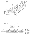
- Exemplary of waveguide means suitable for use in apparatus according to the invention is a ridge waveguide as is schematically depicted in FIG. 2, wherein numeral 21 refers to the Si substrate, 22 to a core layer (e.g., comprising at least 90 atomic % SiGe alloy having effective refractive index greater than that of Si, and 23 to a cladding layer, e.g., SiO2 or Si. Numeral 24 refers to the ridge whose presence provides lateral guiding of the radiation. It will be appreciated that in devices according to the invention at least a portion of layer 22 (typically the portion underlying ridge 24) is doped with the appropriate rare earth ions and the co-dopant or co-dopants. Such an optical waveguide can be produced by known procedures.
- III-V semiconductors can be used to manufacture optical gain devices, their thermal conductivity typically is relatively low, limiting the pumping energy (radiation or electrical current) that can be dissipated.
- Si has relatively high thermal conductivity, making it possible to construct relatively long (e.g., of order 1 cm) devices according to the invention. This is expected to, inter alia, facilitate design and manufacture of devices capable of providing significant gain for signal radiation of the wavelength or wavelengths of interest herein.
- FIG. 3 schematically shows an electrically pumped device 30 according to the invention.
- a structurally similar device, suitable for intensity modulation of 1.55 ⁇ m radiation, has been disclosed by R. D. Lumble et al., Electronics Letters , Vol. 26 (20), pp. 1653-1655.
- numeral 31 refers to the single crystal Si substrate (exemplarily doped n+); 32 to the epitaxial Si lower cladding layer (exemplarily doped n); 33 to the epitaxial SiGe alloy core layer (exemplarily p-doped Ge 0.2 Si 0.8 ); and 34 to the epitaxial Si top cladding layer (exemplarily doped n).
- Layers 35, 36 and 37 are metal contact layers that facilitate electrical pumping of the device, with consequent amplification of the radiation coupled into the device.
- core layer 33 comprises RE and a co-dopant according to the invention, and optionally comprises oxygen.
- electrically pumped embodiments of the invention do not necessarily involve three-terminal devices as shown in FIG. 3, and that a two-terminal p-n structure also has utility.
- Such a device can be produced by a generally conventional process that is modified to include implantation of the co-dopant or co-dopants.
- FIG. 4 depicts schematically a portion 40 of an exemplary optical fiber transmission system according to the invention, wherein radiation is transmitted from some generation means (not shown) through optical fiber 41 to amplification means that comprise coupling means 42 (comprising, e.g., focusing means such as a spherical lens) that serve to couple the radiation into the appropriately doped core of inventive planar optical amplifier 43.
- coupling means 42 comprising, e.g., focusing means such as a spherical lens
- the radiation is amplified by stimulated emission, the pump energy derived from pump source 47 (typically an electrical power supply).
- Optional coupling means 44 serve to couple the amplified radiation into utilization means, exemplarily star coupler 45 serving to divide the radiation into n outputs that are coupled into n optical fibers 461-46n.
- the signals are transmitted through said fibers to some appropriate utilization means, e.g., an optical detector on a subscriber premise.
- amplification means according to the invention may be utilized in optical computing means.
- devices according to the invention can serve as radiation sources, namely, as lasers or LEDs.
Landscapes
- Physics & Mathematics (AREA)
- Condensed Matter Physics & Semiconductors (AREA)
- General Physics & Mathematics (AREA)
- Electromagnetism (AREA)
- Optics & Photonics (AREA)
- Lasers (AREA)
- Semiconductor Lasers (AREA)
- Optical Integrated Circuits (AREA)
- Led Device Packages (AREA)
- Led Devices (AREA)
Applications Claiming Priority (2)
| Application Number | Priority Date | Filing Date | Title |
|---|---|---|---|
| US07/711,243 US5107538A (en) | 1991-06-06 | 1991-06-06 | Optical waveguide system comprising a rare-earth Si-based optical device |
| US711243 | 1991-06-06 |
Publications (3)
| Publication Number | Publication Date |
|---|---|
| EP0517440A2 true EP0517440A2 (fr) | 1992-12-09 |
| EP0517440A3 EP0517440A3 (en) | 1993-01-20 |
| EP0517440B1 EP0517440B1 (fr) | 1994-12-28 |
Family
ID=24857304
Family Applications (1)
| Application Number | Title | Priority Date | Filing Date |
|---|---|---|---|
| EP92304896A Expired - Lifetime EP0517440B1 (fr) | 1991-06-06 | 1992-05-29 | Article ou système comprenant un dispositif optique à base de silicium |
Country Status (4)
| Country | Link |
|---|---|
| US (1) | US5107538A (fr) |
| EP (1) | EP0517440B1 (fr) |
| JP (1) | JPH081974B2 (fr) |
| DE (1) | DE69201013T2 (fr) |
Cited By (8)
| Publication number | Priority date | Publication date | Assignee | Title |
|---|---|---|---|---|
| EP0799495A4 (fr) * | 1994-11-10 | 1999-11-03 | Lawrence Semiconductor Researc | Compositions silicium-germanium-carbone et processus associes |
| EP1081812A1 (fr) * | 1999-09-02 | 2001-03-07 | STMicroelectronics S.r.l. | Dispositif semi-conducteur pour utilisation électro-optique, méthode de fabrication et dispositif laser à semi-conducteur |
| EP0945938A3 (fr) * | 1998-02-25 | 2001-07-25 | International Business Machines Corporation | Pompage électrique de silicium dopé par des terres rares pour émission optique |
| WO2002013243A3 (fr) * | 2000-08-08 | 2003-03-13 | Translucent Photonics Inc | Dispositifs servant a obtenir un gain optique dans du silicium |
| US6570187B1 (en) | 1999-02-10 | 2003-05-27 | Commissariat a l′Energie Atomique | Silicon light-emitting device and method for the production thereof |
| WO2003096437A3 (fr) * | 2002-05-06 | 2004-02-05 | Intel Corp | Dispositif electroluminescent de silicium et de silicium/germanium, procedes et systemes associes |
| EP1196954A4 (fr) * | 1999-04-23 | 2006-10-04 | Univ Cincinnati | Dispositif emetteur de lumiere visible, forme a partir d'un semi-conducteur a large bande interdite, dope a l'aide d'un element en terres rares |
| RU2407109C1 (ru) * | 2009-10-05 | 2010-12-20 | Учреждение Российской академии наук Институт физики микроструктур РАН | Полупроводниковый светоизлучающий прибор |
Families Citing this family (67)
| Publication number | Priority date | Publication date | Assignee | Title |
|---|---|---|---|---|
| DE4022090A1 (de) * | 1989-12-18 | 1991-06-20 | Forschungszentrum Juelich Gmbh | Elektro-optisches bauelement und verfahren zu dessen herstellung |
| DE4011860A1 (de) * | 1990-04-09 | 1991-10-10 | Siemens Ag | Halbleiterelement mit einer silizium-schicht |
| JP2755471B2 (ja) * | 1990-06-29 | 1998-05-20 | 日立電線株式会社 | 希土類元素添加光導波路及びその製造方法 |
| FR2675592B1 (fr) * | 1991-04-22 | 1993-07-16 | Alcatel Nv | Amplificateur optique dans le domaine spectral 1,26 a 1,34 mum. |
| FR2685135B1 (fr) * | 1991-12-16 | 1994-02-04 | Commissariat A Energie Atomique | Mini cavite laser pompee optiquement, son procede de fabrication et laser utilisant cette cavite. |
| US5322813A (en) * | 1992-08-31 | 1994-06-21 | International Business Machines Corporation | Method of making supersaturated rare earth doped semiconductor layers by chemical vapor deposition |
| US5369657A (en) * | 1992-09-15 | 1994-11-29 | Texas Instruments Incorporated | Silicon-based microlaser by doped thin films |
| US5384795A (en) * | 1992-09-15 | 1995-01-24 | Texas Instruments Incorporated | Light emission from rare-earth element-doped CaF2 thin films by electroluminescence |
| JPH06203959A (ja) * | 1992-09-30 | 1994-07-22 | Texas Instr Inc <Ti> | エレクトロルミネセンスによりNdでドープされたCaF2薄膜から発光せしめる装置および方法 |
| US5259046A (en) * | 1992-10-01 | 1993-11-02 | At&T Bell Laboratories | Article comprising an optical waveguide containing a fluorescent dopant |
| JPH087286B2 (ja) * | 1992-10-28 | 1996-01-29 | インターナショナル・ビジネス・マシーンズ・コーポレイション | 光導波管装置 |
| JP3377794B2 (ja) * | 1993-09-21 | 2003-02-17 | ブッカム・テクノロジイ・ピイエルシイ | 電気光学デバイス |
| US5491768A (en) * | 1994-07-27 | 1996-02-13 | The Chinese University Of Hong Kong | Optical waveguide employing modified gallium arsenide |
| US5548128A (en) * | 1994-12-14 | 1996-08-20 | The United States Of America As Represented By The Secretary Of The Air Force | Direct-gap germanium-tin multiple-quantum-well electro-optical devices on silicon or germanium substrates |
| US6233070B1 (en) | 1998-05-19 | 2001-05-15 | Bookham Technology Plc | Optical system and method for changing the lengths of optical paths and the phases of light beams |
| US6351578B1 (en) * | 1999-08-06 | 2002-02-26 | Gemfire Corporation | Thermo-optic switch having fast rise-time |
| JP2001135893A (ja) | 1999-11-05 | 2001-05-18 | Fujitsu Ltd | 光半導体装置および光電子集積回路装置 |
| JP5054874B2 (ja) * | 1999-12-02 | 2012-10-24 | ティーガル コーポレイション | リアクタ内でプラチナエッチングを行う方法 |
| US6506289B2 (en) | 2000-08-07 | 2003-01-14 | Symmorphix, Inc. | Planar optical devices and methods for their manufacture |
| US6533907B2 (en) | 2001-01-19 | 2003-03-18 | Symmorphix, Inc. | Method of producing amorphous silicon for hard mask and waveguide applications |
| US7469558B2 (en) * | 2001-07-10 | 2008-12-30 | Springworks, Llc | As-deposited planar optical waveguides with low scattering loss and methods for their manufacture |
| US7404877B2 (en) * | 2001-11-09 | 2008-07-29 | Springworks, Llc | Low temperature zirconia based thermal barrier layer by PVD |
| US7290407B1 (en) | 2001-12-19 | 2007-11-06 | Jesse Chienhua Shan | Triangle-shaped planar optical waveguide having reduced scattering loss |
| US6884327B2 (en) * | 2002-03-16 | 2005-04-26 | Tao Pan | Mode size converter for a planar waveguide |
| US7378356B2 (en) * | 2002-03-16 | 2008-05-27 | Springworks, Llc | Biased pulse DC reactive sputtering of oxide films |
| US20030175142A1 (en) * | 2002-03-16 | 2003-09-18 | Vassiliki Milonopoulou | Rare-earth pre-alloyed PVD targets for dielectric planar applications |
| US8431264B2 (en) | 2002-08-09 | 2013-04-30 | Infinite Power Solutions, Inc. | Hybrid thin-film battery |
| US8445130B2 (en) | 2002-08-09 | 2013-05-21 | Infinite Power Solutions, Inc. | Hybrid thin-film battery |
| US8021778B2 (en) | 2002-08-09 | 2011-09-20 | Infinite Power Solutions, Inc. | Electrochemical apparatus with barrier layer protected substrate |
| US8236443B2 (en) | 2002-08-09 | 2012-08-07 | Infinite Power Solutions, Inc. | Metal film encapsulation |
| US8404376B2 (en) | 2002-08-09 | 2013-03-26 | Infinite Power Solutions, Inc. | Metal film encapsulation |
| US20070264564A1 (en) | 2006-03-16 | 2007-11-15 | Infinite Power Solutions, Inc. | Thin film battery on an integrated circuit or circuit board and method thereof |
| US7993773B2 (en) | 2002-08-09 | 2011-08-09 | Infinite Power Solutions, Inc. | Electrochemical apparatus with barrier layer protected substrate |
| US8394522B2 (en) | 2002-08-09 | 2013-03-12 | Infinite Power Solutions, Inc. | Robust metal film encapsulation |
| AU2003261463A1 (en) * | 2002-08-27 | 2004-03-19 | Symmorphix, Inc. | Optically coupling into highly uniform waveguides |
| US7205662B2 (en) | 2003-02-27 | 2007-04-17 | Symmorphix, Inc. | Dielectric barrier layer films |
| US8728285B2 (en) | 2003-05-23 | 2014-05-20 | Demaray, Llc | Transparent conductive oxides |
| US7238628B2 (en) * | 2003-05-23 | 2007-07-03 | Symmorphix, Inc. | Energy conversion and storage films and devices by physical vapor deposition of titanium and titanium oxides and sub-oxides |
| WO2005002006A2 (fr) * | 2003-06-30 | 2005-01-06 | University Of Cincinnati | Amplificateur de guide d'ondes electroluminescent a base d'impuretes et procedes d'amplification de signaux de donnees optiques |
| JP2005116709A (ja) * | 2003-10-06 | 2005-04-28 | Sony Corp | 半導体集積回路装置およびその製造方法 |
| US7440180B2 (en) * | 2004-02-13 | 2008-10-21 | Tang Yin S | Integration of rare-earth doped amplifiers into semiconductor structures and uses of same |
| JP2006133723A (ja) * | 2004-10-08 | 2006-05-25 | Sony Corp | 光導波モジュール及び光・電気複合デバイス、並びにこれらの製造方法 |
| KR101127370B1 (ko) | 2004-12-08 | 2012-03-29 | 인피니트 파워 솔루션스, 인크. | LiCoO2의 증착 |
| US7959769B2 (en) | 2004-12-08 | 2011-06-14 | Infinite Power Solutions, Inc. | Deposition of LiCoO2 |
| JP2008526003A (ja) * | 2004-12-24 | 2008-07-17 | ピレリ・アンド・チ・ソチエタ・ペル・アツィオーニ | ゲルマニウムオンシリコンの光検出器 |
| US7037806B1 (en) * | 2005-02-09 | 2006-05-02 | Translucent Inc. | Method of fabricating silicon-on-insulator semiconductor substrate using rare earth oxide or rare earth nitride |
| JP2006332137A (ja) * | 2005-05-23 | 2006-12-07 | Nippon Telegr & Teleph Corp <Ntt> | 発光素子 |
| US7838133B2 (en) * | 2005-09-02 | 2010-11-23 | Springworks, Llc | Deposition of perovskite and other compound ceramic films for dielectric applications |
| KR101455404B1 (ko) * | 2005-12-09 | 2014-10-27 | 세미이큅, 인코포레이티드 | 탄소 클러스터의 주입에 의한 반도체 디바이스의 제조를위한 시스템 및 방법 |
| US20090015906A1 (en) * | 2006-05-18 | 2009-01-15 | Kimerling Lionel C | Extrinsic gain laser and optical amplification device |
| CN101523571A (zh) | 2006-09-29 | 2009-09-02 | 无穷动力解决方案股份有限公司 | 柔性基板上沉积的电池层的掩模和材料限制 |
| US8197781B2 (en) | 2006-11-07 | 2012-06-12 | Infinite Power Solutions, Inc. | Sputtering target of Li3PO4 and method for producing same |
| US7919402B2 (en) * | 2006-12-06 | 2011-04-05 | Semequip, Inc. | Cluster ion implantation for defect engineering |
| US8144392B2 (en) * | 2007-02-12 | 2012-03-27 | The United States Of America As Represented By The Secretary Of The Navy | Waveguide amplifier in a sputtered film of erbium-doped gallium lanthanum sulfide glass |
| TWI474382B (zh) * | 2007-04-11 | 2015-02-21 | 山米奎普公司 | 用於缺陷工程的簇離子植入 |
| US8268488B2 (en) | 2007-12-21 | 2012-09-18 | Infinite Power Solutions, Inc. | Thin film electrolyte for thin film batteries |
| CN101903560B (zh) | 2007-12-21 | 2014-08-06 | 无穷动力解决方案股份有限公司 | 用于电解质膜的溅射靶的方法 |
| US8518581B2 (en) | 2008-01-11 | 2013-08-27 | Inifinite Power Solutions, Inc. | Thin film encapsulation for thin film batteries and other devices |
| WO2009124191A2 (fr) | 2008-04-02 | 2009-10-08 | Infinite Power Solutions, Inc. | Commande de sur/sous tension passive et protection pour des dispositifs de stockage d’énergie associés à un captage d’énergie |
| JP2012500610A (ja) * | 2008-08-11 | 2012-01-05 | インフィニット パワー ソリューションズ, インコーポレイテッド | 電磁エネルギー獲得ための統合コレクタ表面を有するエネルギーデバイスおよびその方法 |
| CN102150185B (zh) | 2008-09-12 | 2014-05-28 | 无穷动力解决方案股份有限公司 | 具有经由电磁能进行数据通信的组成导电表面的能量装置及其方法 |
| WO2010042594A1 (fr) | 2008-10-08 | 2010-04-15 | Infinite Power Solutions, Inc. | Module de capteurs sans fil alimenté par l’environnement |
| CN102576828B (zh) | 2009-09-01 | 2016-04-20 | 萨普拉斯特研究有限责任公司 | 具有集成薄膜电池的印刷电路板 |
| EP2577777B1 (fr) | 2010-06-07 | 2016-12-28 | Sapurast Research LLC | Dispositif électrochimique à haute densité rechargeable |
| JP5831165B2 (ja) | 2011-11-21 | 2015-12-09 | 富士通株式会社 | 半導体光素子 |
| CN103219646A (zh) * | 2013-03-21 | 2013-07-24 | 常州镭赛科技有限公司 | 光放大器 |
| CN110429474B (zh) * | 2019-07-31 | 2021-05-14 | 天津工业大学 | 一种全四族硅基c波段半导体激光器 |
Family Cites Families (11)
| Publication number | Priority date | Publication date | Assignee | Title |
|---|---|---|---|---|
| DE3319134A1 (de) * | 1983-05-26 | 1985-05-02 | Fraunhofer-Gesellschaft zur Förderung der angewandten Forschung e.V., 8000 München | Optoelektronisches bauelement, insbesondere eine laserdiode oder eine leuchtdiode |
| JPS60114811A (ja) * | 1983-11-28 | 1985-06-21 | Hitachi Ltd | 光導波路およびその製造方法 |
| US4575919A (en) * | 1984-05-24 | 1986-03-18 | At&T Bell Laboratories | Method of making heteroepitaxial ridge overgrown laser |
| GB8724736D0 (en) * | 1987-10-22 | 1987-11-25 | British Telecomm | Optical fibre |
| US5023885A (en) * | 1988-09-20 | 1991-06-11 | Siemens Aktiengesellschaft | External optical resonator for a semiconductor laser |
| US4962995A (en) * | 1989-06-16 | 1990-10-16 | Gte Laboratories Incorporated | Glasses for high efficiency erbium (3+) optical fiber lasers, amplifiers, and superluminescent sources |
| JPH0373934A (ja) * | 1989-08-15 | 1991-03-28 | Fujitsu Ltd | 光増幅器 |
| US5005175A (en) * | 1989-11-27 | 1991-04-02 | At&T Bell Laboratories | Erbium-doped fiber amplifier |
| US5027079A (en) * | 1990-01-19 | 1991-06-25 | At&T Bell Laboratories | Erbium-doped fiber amplifier |
| JPH0644645B2 (ja) * | 1990-03-30 | 1994-06-08 | ホーヤ株式会社 | 光導波路型レーザ媒体及び光導波路型レーザ装置 |
| US5039190A (en) * | 1990-09-07 | 1991-08-13 | At&T Bell Laboratories | Apparatus comprising an optical gain device, and method of producing the device |
-
1991
- 1991-06-06 US US07/711,243 patent/US5107538A/en not_active Expired - Lifetime
-
1992
- 1992-05-11 JP JP14364492A patent/JPH081974B2/ja not_active Expired - Lifetime
- 1992-05-29 DE DE69201013T patent/DE69201013T2/de not_active Expired - Fee Related
- 1992-05-29 EP EP92304896A patent/EP0517440B1/fr not_active Expired - Lifetime
Cited By (17)
| Publication number | Priority date | Publication date | Assignee | Title |
|---|---|---|---|---|
| EP0799495A4 (fr) * | 1994-11-10 | 1999-11-03 | Lawrence Semiconductor Researc | Compositions silicium-germanium-carbone et processus associes |
| EP0945938A3 (fr) * | 1998-02-25 | 2001-07-25 | International Business Machines Corporation | Pompage électrique de silicium dopé par des terres rares pour émission optique |
| KR100377716B1 (ko) * | 1998-02-25 | 2003-03-26 | 인터내셔널 비지네스 머신즈 코포레이션 | 광학적 방사를 위해 희토류 원소로 도핑된 실리콘 구조체 및 방사방법 |
| US6570187B1 (en) | 1999-02-10 | 2003-05-27 | Commissariat a l′Energie Atomique | Silicon light-emitting device and method for the production thereof |
| EP1196954A4 (fr) * | 1999-04-23 | 2006-10-04 | Univ Cincinnati | Dispositif emetteur de lumiere visible, forme a partir d'un semi-conducteur a large bande interdite, dope a l'aide d'un element en terres rares |
| US6828598B1 (en) | 1999-09-02 | 2004-12-07 | Stmicroelectronics S.R.L. | Semiconductor device for electro-optic applications, method for manufacturing said device and corresponding semiconductor laser device |
| EP1081812A1 (fr) * | 1999-09-02 | 2001-03-07 | STMicroelectronics S.r.l. | Dispositif semi-conducteur pour utilisation électro-optique, méthode de fabrication et dispositif laser à semi-conducteur |
| WO2001017074A1 (fr) * | 1999-09-02 | 2001-03-08 | Stmicroelectronics S.R.L. | Dispositif a semi-conducteur pour applications electrooptiques, son procede de fabrication et laser a semi-conducteur correspondant |
| WO2002013243A3 (fr) * | 2000-08-08 | 2003-03-13 | Translucent Photonics Inc | Dispositifs servant a obtenir un gain optique dans du silicium |
| US6734453B2 (en) | 2000-08-08 | 2004-05-11 | Translucent Photonics, Inc. | Devices with optical gain in silicon |
| US6858864B2 (en) | 2000-08-08 | 2005-02-22 | Translucent Photonics, Inc. | Devices with optical gain in silicon |
| US7135699B1 (en) | 2000-08-08 | 2006-11-14 | Translucent Photonics, Inc. | Method and apparatus for growth of single-crystal rare-earth oxides, nitrides, and phosphides |
| US7211821B2 (en) | 2000-08-08 | 2007-05-01 | Translucent Photonics, Inc. | Devices with optical gain in silicon |
| US6924510B2 (en) | 2002-05-06 | 2005-08-02 | Intel Corporation | Silicon and silicon/germanium light-emitting device, methods and systems |
| WO2003096437A3 (fr) * | 2002-05-06 | 2004-02-05 | Intel Corp | Dispositif electroluminescent de silicium et de silicium/germanium, procedes et systemes associes |
| US7169631B2 (en) | 2002-05-06 | 2007-01-30 | Intel Corporation | Silicon and silicon/germanium light-emitting device, methods and systems |
| RU2407109C1 (ru) * | 2009-10-05 | 2010-12-20 | Учреждение Российской академии наук Институт физики микроструктур РАН | Полупроводниковый светоизлучающий прибор |
Also Published As
| Publication number | Publication date |
|---|---|
| JPH05175592A (ja) | 1993-07-13 |
| EP0517440A3 (en) | 1993-01-20 |
| US5107538A (en) | 1992-04-21 |
| DE69201013T2 (de) | 1995-05-11 |
| EP0517440B1 (fr) | 1994-12-28 |
| JPH081974B2 (ja) | 1996-01-10 |
| DE69201013D1 (de) | 1995-02-09 |
Similar Documents
| Publication | Publication Date | Title |
|---|---|---|
| EP0517440B1 (fr) | Article ou système comprenant un dispositif optique à base de silicium | |
| Thaik et al. | Photoluminescence spectroscopy of erbium implanted gallium nitride | |
| Wilson et al. | 1.54‐μm photoluminescence from Er‐implanted GaN and AlN | |
| Miyajima et al. | 38.2 dB amplification at 1.31 μm and possibility of 0.98 μm pumping in Pr3+-doped fluoride fibre | |
| US5077143A (en) | Silicon electroluminescent device | |
| EP0261875B1 (fr) | Laser à semi-conducteur à dopage de terre rare | |
| Jantsch et al. | Different Er centres in Si and their use for electroluminescent devices | |
| EP1210752B9 (fr) | Laser a semi-conducteur pour applications electrooptiques et son procede de fabrication | |
| US6570187B1 (en) | Silicon light-emitting device and method for the production thereof | |
| Reed et al. | Erbium-doped silicon and porous silicon for optoelectronics | |
| McFarlane et al. | Rare earth doped fluoride waveguides fabricated using molecular beam epitaxy | |
| KR100377716B1 (ko) | 광학적 방사를 위해 희토류 원소로 도핑된 실리콘 구조체 및 방사방법 | |
| US5045498A (en) | Method of fabricating an atomic element doped semiconductor injection laser using ion implantation and epitaxial growth on the implanted surface | |
| Priolo et al. | Optical doping of materials by erbium ion implantation | |
| US4821274A (en) | Electro-optical semiconductor device and a method of emitting light | |
| Bondarenko et al. | Luminescence of erbium-doped porous silicon. | |
| Zhou et al. | Room-temperature 2 μm luminescence from Tm doped silicon light emitting diodes and SOI substrates | |
| Jantsch et al. | Status, Hopes and Limitations for the Si: Er-based 1.54 μm Emitter | |
| Pearton et al. | Er-doping of gan and related alloys | |
| Wittke | Thin-film lasers | |
| Shiryaev et al. | Development of mid-IR chalcogenide fiber emitters | |
| Zavada | Rare earth impurities in wide gap semiconductors | |
| Peaker | Erbium in semiconductors: where are we coming from; where are we going? | |
| Zavada et al. | Near infrared photonic devices based on Er-doped GaN and InGaN | |
| Seo et al. | Rare-earth-doped nanocrystalline silicon: excitation and de-excitation mechanisms and implications for waveguide amplifier applications |
Legal Events
| Date | Code | Title | Description |
|---|---|---|---|
| PUAI | Public reference made under article 153(3) epc to a published international application that has entered the european phase |
Free format text: ORIGINAL CODE: 0009012 |
|
| PUAL | Search report despatched |
Free format text: ORIGINAL CODE: 0009013 |
|
| AK | Designated contracting states |
Kind code of ref document: A2 Designated state(s): DE FR GB |
|
| AK | Designated contracting states |
Kind code of ref document: A3 Designated state(s): DE FR GB |
|
| 17P | Request for examination filed |
Effective date: 19930708 |
|
| 17Q | First examination report despatched |
Effective date: 19940124 |
|
| RAP3 | Party data changed (applicant data changed or rights of an application transferred) |
Owner name: AT&T CORP. |
|
| GRAA | (expected) grant |
Free format text: ORIGINAL CODE: 0009210 |
|
| AK | Designated contracting states |
Kind code of ref document: B1 Designated state(s): DE FR GB |
|
| REF | Corresponds to: |
Ref document number: 69201013 Country of ref document: DE Date of ref document: 19950209 |
|
| ET | Fr: translation filed | ||
| PLBE | No opposition filed within time limit |
Free format text: ORIGINAL CODE: 0009261 |
|
| STAA | Information on the status of an ep patent application or granted ep patent |
Free format text: STATUS: NO OPPOSITION FILED WITHIN TIME LIMIT |
|
| 26N | No opposition filed | ||
| REG | Reference to a national code |
Ref country code: GB Ref legal event code: IF02 |
|
| PGFP | Annual fee paid to national office [announced via postgrant information from national office to epo] |
Ref country code: FR Payment date: 20090513 Year of fee payment: 18 Ref country code: DE Payment date: 20090525 Year of fee payment: 18 |
|
| PGFP | Annual fee paid to national office [announced via postgrant information from national office to epo] |
Ref country code: GB Payment date: 20090522 Year of fee payment: 18 |
|
| GBPC | Gb: european patent ceased through non-payment of renewal fee |
Effective date: 20100529 |
|
| REG | Reference to a national code |
Ref country code: FR Ref legal event code: ST Effective date: 20110131 |
|
| PG25 | Lapsed in a contracting state [announced via postgrant information from national office to epo] |
Ref country code: DE Free format text: LAPSE BECAUSE OF NON-PAYMENT OF DUE FEES Effective date: 20101201 |
|
| PG25 | Lapsed in a contracting state [announced via postgrant information from national office to epo] |
Ref country code: FR Free format text: LAPSE BECAUSE OF NON-PAYMENT OF DUE FEES Effective date: 20100531 |
|
| PG25 | Lapsed in a contracting state [announced via postgrant information from national office to epo] |
Ref country code: GB Free format text: LAPSE BECAUSE OF NON-PAYMENT OF DUE FEES Effective date: 20100529 |