EP0517560A2 - Méthode de fabrication d'un substrat utilisé dans un dispositif micro-ondes supraconducteur - Google Patents
Méthode de fabrication d'un substrat utilisé dans un dispositif micro-ondes supraconducteur Download PDFInfo
- Publication number
- EP0517560A2 EP0517560A2 EP92401374A EP92401374A EP0517560A2 EP 0517560 A2 EP0517560 A2 EP 0517560A2 EP 92401374 A EP92401374 A EP 92401374A EP 92401374 A EP92401374 A EP 92401374A EP 0517560 A2 EP0517560 A2 EP 0517560A2
- Authority
- EP
- European Patent Office
- Prior art keywords
- substrate
- annealing
- underlying substrate
- thin film
- thallium
- Prior art date
- Legal status (The legal status is an assumption and is not a legal conclusion. Google has not performed a legal analysis and makes no representation as to the accuracy of the status listed.)
- Granted
Links
Images
Classifications
-
- H—ELECTRICITY
- H10—SEMICONDUCTOR DEVICES; ELECTRIC SOLID-STATE DEVICES NOT OTHERWISE PROVIDED FOR
- H10N—ELECTRIC SOLID-STATE DEVICES NOT OTHERWISE PROVIDED FOR
- H10N60/00—Superconducting devices
- H10N60/01—Manufacture or treatment
- H10N60/0268—Manufacture or treatment of devices comprising copper oxide
- H10N60/0661—Processes performed after copper oxide formation, e.g. patterning
Definitions
- the present invention relates to a method for manufacturing a substrate for a superconducting microwave component, and more specifically to a novel method for manufacturing a substrate which can be suitably used in fabricating an microwave component having a conductor formed of an oxide superconducting thin film.
- Electromagnetic waves called "microwaves” or “millimetric waves” having a wavelength in a range of a few tens centimeters to a few millimeters can be theoretically said to be merely a part of an electromagnetic wave spectrum, but have been considered from a viewpoint of an electric engineering to be a special independent field of the electromagnetic wave, since special and unique methods and devices have been developed for handling these electromagnetic waves.
- a microstrip line has an attenuation coefficient that is attributable to a resistance component of the conductor. This attenuation coefficient attributable to the resistance component increases in proportion to a root of a frequency.
- the dielectric loss increases in proportion to increase of the frequency.
- the loss of a recent microstrip line particularly in the range of not greater than 10 GHz is almost attributable to the resistance of the conductor, since the dielectric materials have been recently improved. Therefore, if the resistance of the conductor in the strip line can be reduced, it is possible to greatly elevate the performance of the microstrip line.
- the microstrip line can be used as a simple signal transmission line. However, if a suitable patterning is applied, the microstrip line can be used as other microwave components including an inductor, a filter, a resonator, and a delayed line. Therefore, improvement of the microstrip line will directly result in improvement of characteristics of these microwave components. Under this circumstance, various microwave devices having a conductor line or lines formed of oxide superconductors have been proposed.
- a microwave transmission line for guiding the electromagnetic waves in the microwave band is generally formed of a pair of conductors separated from each other by a dielectric, one of the pair of conductors being grounded.
- a substrate which can be suitably used in fabricating the above mentioned microwave transmission line is formed of a dielectric substrate as an underlying substrate and a pair of oxide superconductor thin films formed on an upper surface and a lower surface of said underlying substrate, respectively. If this substrate is given or available, various superconduction microwave components can be easily fabricated by suitably patterning one of the pair of oxide superconductor thin films formed on the upper and lower surfaces of said underlying substrate, respectively.
- the oxide superconductor thin film can be obtained only when a film of oxide superconductor material is deposited on a specific substrate under a specific deposition condition.
- oxygen contained in the oxide superconductor material is unstable, if the deposited oxide superconductor material is heated, the content of the oxygen will change. Therefore, in the process of sequentially depositing an oxide superconductor thin film on one or first surface of a dielectric substrate, and thereafter on the other or second surface of the dielectric substrate, the superconductor characteristics of the oxide superconductor thin film deposited on the first surface of a dielectric substrate is deteriorated or lost when the oxide superconductor thin film is deposited on the second surface of a dielectric substrate. Because of this, it has been considered difficult to prepare a substrate for microwave component having superconductor thin film of uniform characteristics formed on opposite surfaces of the dielectric substrate.
- a method for manufacturing a substrate for a superconducting microwave component the substrate being composed of an underlying substrate including a dielectric layer, and a pair of oxide superconductor thin films formed on an upper surface and a lower surface of the underlying substrate, respectively, characterrized by the steps of forming a Tl-Ba-Ca-Cu-O compound oxide thin film on one surface of the underlying substrate, forming another Tl-Ba-Ca-Cu-O compound oxide thin film on the other surface of the underlying substrate, and annealing in a thallium atmosphere the underlying substrate having a pair of surfaces coated with the Tl-Ba-Ca-Cu-O compound oxide thin films.
- the method in accordance with present invention for manufacturing a substrate for a superconducting microwave component is characterized in that after the Tl-type compound oxide thin films are formed on the opposite surfaces of the underlying substrate, respectively, the formed Tl-type compound oxide thin films are annealed in the thallium atmosphere.
- the deterioration of the superconductor characteristics of the oxide superconductor thin film deposited on the first surface of the underlying substrate is inevitable in the step of depositing the oxide superconductor thin film on the second surface of the underlying substrate.
- the Tl-type compound oxide is used as the oxide superconductor material, it is possible to perform the process for finally restoring the characteristics of the pair of oxide superconductor thin film.
- the Tl-type oxide superconducting thin films at an extremely low substrate temperature on the order of a room temperature. Therefore, in the case that an oxide superconducting thin film is formed on one surface of the underlying substrate and thereafter on the other surface of the underlying substrate, the deterioration of the firstly deposited thin film can be minimized.
- the quality of the film can be improved.
- the deposited Tl-type oxide superconducting thin films are annealed in the thallium atmosphere, not only the quality of the pair of Tl-type oxide superconducting thin films can be improved, but also the film characteristics of the pair of thin films can be brought into substantially the same.
- the annealing is preferably conducted in an oxygen atmosphere containing not less than 5 mol % of thallium. If the content of the thallium is less than 5 mol %, an effective improvement of the film quality due to the annealing cannot be obtained. In this connection, it is considered that when the thallium is contained in the annealing oxygen atmosphere, the thallium exists in the form of thallium oxide.
- the annealing temperature is preferred to be in the range of 850°C to 900°C inclusive. If the annealing temperature is lower than this temperature range, a valid annealing effect cannot be obtained. If the annealing temperature is higher than this temperature range, the film quality of the thin film is rather deteriorated due to the annealing heat.
- the annealing period of time is preferred to be in the range of one hour to three hours inclusive. If the annealing time is shorter than this range, a valid annealing effect cannot be obtained. If the annealing time is longer than this range, the film quality of the thin film is rather deteriorated due to the annealing heat.
- the underlying substrate should be formed of a dielectric material which has a small dielectric loss and which makes it possible to deposit the oxide superconductor thin film thereon in a good condition.
- LaAlO3, NdGaO3 and MgO can be exemplified.
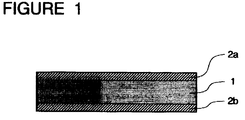
- Figure 1 is a diagrammatic sectional view illustrating a basic construction of the substrate for the superconducting microwave component.
- the substrate for the superconducting microwave component includes a dielectric underlying substrate 1 and a pair of oxide superconducting thin films 2a and 2b deposited on opposite surfaces of the underlying substrate 1, respectively.
- the superconducting microwave component substrate having the above mentioned construction was manufactured in accordance with the method of the present invention.
- a LaAlO3 substrate having a thickness of 0.5 mm, a width of 15 mm and a length of 15 mm was used as the dielectric substrate.
- An oxide superconducting thin film was deposited by sputtering. The deposition condition was as follows:
- a pair of oxide superconducting thin films were continuously deposited on opposite surfaces of the dielectric substrate, respectively, in the same deposition chamber without taking the substrate out of the deposition chamber.
- the substrate having the opposite surfaces coated with the oxide superconducting thin films, respectively was annealed in a thallium atmosphere.
- the annealing condition was as follows:
- the characteristics of the oxide superconductor thin film formed on each of the opposite surfaces was measured.
- the result of the measurement is shown in the following:
- the oxide superconductor thin films respectively formed on the opposite surfaces of the underlying substrate have a substantially uniform superconduction characteristics.
- the critical current density was measured at 77 K.
- Example 2 For comparison, another substrate for microwave component was manufactured by using the same dielectric substrate as that of Example 1, and using an Y-Ba-Cu-O type compound oxide superconducting thin film material.
- the Y-Ba-Cu-O type compound oxide superconducting thin film was deposited by a sputtering. The deposition condition was as follows:
- the oxide superconductor thin film formed on the first surface of the underlying substrate was remarkably deteriorated in characteristics.
- the critical current density was measured at 77 K.
- a substrate for microwave component was manufactured in the same process as that of Example 1, excluding the annealing condition.
- the substrate thus manufactured was annealed in a thallium atmosphere under the following annealing condition:
- the characteristics of the oxide superconductor thin film formed on each of the opposite surfaces was measured.
- the critical current density was measured at 77 K. The result of the measurement is shown in the following:
- a substrate for microwave component was manufactured in the same process as that of Example 1, excluding the annealing condition.
- the substrate thus manufactured was annealed in a thallium atmosphere under the following annealing condition:
- the characteristics of the oxide superconductor thin film formed on each of the opposite surfaces was measured.
- the critical current density was measured at 77 K. The result of the measurement is shown in the following;
- a substrate for microwave component was manufactured in the same process as that of Example 1, excluding the annealing condition.
- the substrate thus manufactured was annealed in a thallium atmosphere under the following annealing condition:
- the characteristics of the oxide superconductor thin film formed on each of the opposite surfaces was measured.
- the critical current density was measured at 77 K. The result of the measurement is shown in the following:
- the substrate manufactured in accordance with the method of the present invention can be used for fabricating various microwave components, by suitably patterning one of the pair of good oxide superconducting thin films.
- the microwave components thus obtained has a conductor formed of the superconductor, and therefore, has a small propagation loss and a wide application frequency band.
Landscapes
- Engineering & Computer Science (AREA)
- Manufacturing & Machinery (AREA)
- Superconductor Devices And Manufacturing Methods Thereof (AREA)
- Superconductors And Manufacturing Methods Therefor (AREA)
- Parts Printed On Printed Circuit Boards (AREA)
- Inorganic Compounds Of Heavy Metals (AREA)
- Physical Vapour Deposition (AREA)
- Manufacturing Of Printed Wiring (AREA)
Applications Claiming Priority (2)
| Application Number | Priority Date | Filing Date | Title |
|---|---|---|---|
| JP3144023A JPH04342487A (ja) | 1991-05-20 | 1991-05-20 | 超電導マイクロ波部品用基板の作製方法 |
| JP144023/91 | 1991-05-20 |
Publications (3)
| Publication Number | Publication Date |
|---|---|
| EP0517560A2 true EP0517560A2 (fr) | 1992-12-09 |
| EP0517560A3 EP0517560A3 (en) | 1993-03-10 |
| EP0517560B1 EP0517560B1 (fr) | 1997-04-02 |
Family
ID=15352532
Family Applications (1)
| Application Number | Title | Priority Date | Filing Date |
|---|---|---|---|
| EP92401374A Expired - Lifetime EP0517560B1 (fr) | 1991-05-20 | 1992-05-20 | Méthode de fabrication d'un substrat utilisé dans un dispositif micro-ondes supraconducteur |
Country Status (3)
| Country | Link |
|---|---|
| EP (1) | EP0517560B1 (fr) |
| JP (1) | JPH04342487A (fr) |
| DE (1) | DE69218665T2 (fr) |
Cited By (1)
| Publication number | Priority date | Publication date | Assignee | Title |
|---|---|---|---|---|
| US8187964B2 (en) | 2007-11-01 | 2012-05-29 | Infineon Technologies Ag | Integrated circuit device and method |
Family Cites Families (1)
| Publication number | Priority date | Publication date | Assignee | Title |
|---|---|---|---|---|
| DE69030365T2 (de) * | 1989-12-22 | 1997-10-23 | Sumitomo Electric Industries | Verfahren zur Herstellung eines supraleitfähigen Mikrowellenbauelements |
-
1991
- 1991-05-20 JP JP3144023A patent/JPH04342487A/ja active Pending
-
1992
- 1992-05-20 EP EP92401374A patent/EP0517560B1/fr not_active Expired - Lifetime
- 1992-05-20 DE DE69218665T patent/DE69218665T2/de not_active Expired - Fee Related
Cited By (1)
| Publication number | Priority date | Publication date | Assignee | Title |
|---|---|---|---|---|
| US8187964B2 (en) | 2007-11-01 | 2012-05-29 | Infineon Technologies Ag | Integrated circuit device and method |
Also Published As
| Publication number | Publication date |
|---|---|
| DE69218665D1 (de) | 1997-05-07 |
| DE69218665T2 (de) | 1997-11-27 |
| EP0517560B1 (fr) | 1997-04-02 |
| JPH04342487A (ja) | 1992-11-27 |
| EP0517560A3 (en) | 1993-03-10 |
Similar Documents
| Publication | Publication Date | Title |
|---|---|---|
| EP0359411B1 (fr) | Matériau de substrat haute-fréquence pour des supraconducteurs à structure en couches du type perovskite, en couches minces | |
| EP0522515B1 (fr) | Résonateur microondes réalisé en matériau supraconducteur d'oxyde composite | |
| EP0280322A2 (fr) | Supra-conducteur céramique en couches | |
| CN1047418A (zh) | 隧道型约瑟夫森器件及其制造方法 | |
| US5604375A (en) | Superconducting active lumped component for microwave device application | |
| EP0516145B1 (fr) | Résonateur hyperfréquence d'un matériau supraconducteur du type oxyde composite | |
| EP0446145A2 (fr) | ProcédÀ© pour préparation des couches minces de supraconducteur de haute température | |
| EP0567407B1 (fr) | Dispositif micro-ondes en matériau supraconducteur d'oxyde | |
| US5428005A (en) | Superconducting thin film of compound oxide and a process of preparing the same | |
| Hermann et al. | Oxide superconductors and ferroelectrics—Materials for a new generation of tunable microwave devices | |
| JP2567517B2 (ja) | 超電導マイクロ波部品 | |
| EP0546904B1 (fr) | Méthode pour fabriquer un dispositif à jonction artificielle de type Josephson à limite de grain | |
| JPH05335638A (ja) | ジョセフソン接合構造体およびその作製方法 | |
| EP0508893A1 (fr) | Substrat pour un composant pour micro-ondes | |
| EP0341148A2 (fr) | Substrat semiconducteur ayant une couche mince supraconductrice | |
| US6156707A (en) | Method of manufacturing superconducting microwave component substrate | |
| EP0517560B1 (fr) | Méthode de fabrication d'un substrat utilisé dans un dispositif micro-ondes supraconducteur | |
| EP0494830B1 (fr) | Méthode pour fabriquer un dispositif à effet Josephson de type à jonction tunnel composé d'un matériau supraconducteur du type oxyde composite | |
| EP0357500B1 (fr) | Procédé pour préparer un film mince supraconducteur de type bismuth | |
| AU655731B2 (en) | Process for preparing superconducting junction of oxide superconductor | |
| JP2850562B2 (ja) | 超電導基板の製造方法 | |
| JP2517085B2 (ja) | 超電導薄膜 | |
| EP0471292B1 (fr) | Substrat pour dispositifs supraconducteurs | |
| US5420103A (en) | A-axis superconductor on a yttrium oxide film | |
| US6610633B1 (en) | Superconductor device |
Legal Events
| Date | Code | Title | Description |
|---|---|---|---|
| PUAI | Public reference made under article 153(3) epc to a published international application that has entered the european phase |
Free format text: ORIGINAL CODE: 0009012 |
|
| AK | Designated contracting states |
Kind code of ref document: A2 Designated state(s): DE FR GB IT |
|
| PUAL | Search report despatched |
Free format text: ORIGINAL CODE: 0009013 |
|
| AK | Designated contracting states |
Kind code of ref document: A3 Designated state(s): DE FR GB IT |
|
| 17P | Request for examination filed |
Effective date: 19930514 |
|
| 17Q | First examination report despatched |
Effective date: 19941026 |
|
| GRAG | Despatch of communication of intention to grant |
Free format text: ORIGINAL CODE: EPIDOS AGRA |
|
| GRAH | Despatch of communication of intention to grant a patent |
Free format text: ORIGINAL CODE: EPIDOS IGRA |
|
| GRAH | Despatch of communication of intention to grant a patent |
Free format text: ORIGINAL CODE: EPIDOS IGRA |
|
| ITF | It: translation for a ep patent filed | ||
| GRAA | (expected) grant |
Free format text: ORIGINAL CODE: 0009210 |
|
| AK | Designated contracting states |
Kind code of ref document: B1 Designated state(s): DE FR GB IT |
|
| REF | Corresponds to: |
Ref document number: 69218665 Country of ref document: DE Date of ref document: 19970507 |
|
| ET | Fr: translation filed | ||
| PLBE | No opposition filed within time limit |
Free format text: ORIGINAL CODE: 0009261 |
|
| STAA | Information on the status of an ep patent application or granted ep patent |
Free format text: STATUS: NO OPPOSITION FILED WITHIN TIME LIMIT |
|
| 26N | No opposition filed | ||
| REG | Reference to a national code |
Ref country code: GB Ref legal event code: IF02 |
|
| PGFP | Annual fee paid to national office [announced via postgrant information from national office to epo] |
Ref country code: FR Payment date: 20030508 Year of fee payment: 12 |
|
| PGFP | Annual fee paid to national office [announced via postgrant information from national office to epo] |
Ref country code: GB Payment date: 20030514 Year of fee payment: 12 |
|
| PGFP | Annual fee paid to national office [announced via postgrant information from national office to epo] |
Ref country code: DE Payment date: 20030529 Year of fee payment: 12 |
|
| PG25 | Lapsed in a contracting state [announced via postgrant information from national office to epo] |
Ref country code: GB Free format text: LAPSE BECAUSE OF NON-PAYMENT OF DUE FEES Effective date: 20040520 |
|
| PG25 | Lapsed in a contracting state [announced via postgrant information from national office to epo] |
Ref country code: DE Free format text: LAPSE BECAUSE OF NON-PAYMENT OF DUE FEES Effective date: 20041201 |
|
| GBPC | Gb: european patent ceased through non-payment of renewal fee |
Effective date: 20040520 |
|
| PG25 | Lapsed in a contracting state [announced via postgrant information from national office to epo] |
Ref country code: FR Free format text: LAPSE BECAUSE OF NON-PAYMENT OF DUE FEES Effective date: 20050131 |
|
| REG | Reference to a national code |
Ref country code: FR Ref legal event code: ST |
|
| PG25 | Lapsed in a contracting state [announced via postgrant information from national office to epo] |
Ref country code: IT Free format text: LAPSE BECAUSE OF NON-PAYMENT OF DUE FEES;WARNING: LAPSES OF ITALIAN PATENTS WITH EFFECTIVE DATE BEFORE 2007 MAY HAVE OCCURRED AT ANY TIME BEFORE 2007. THE CORRECT EFFECTIVE DATE MAY BE DIFFERENT FROM THE ONE RECORDED. Effective date: 20050520 |