EP0518545A1 - Lithographisches Trockenätzverfahren mittels Gasgemischen aus Sauerstoff und Chlor - Google Patents
Lithographisches Trockenätzverfahren mittels Gasgemischen aus Sauerstoff und Chlor Download PDFInfo
- Publication number
- EP0518545A1 EP0518545A1 EP92305052A EP92305052A EP0518545A1 EP 0518545 A1 EP0518545 A1 EP 0518545A1 EP 92305052 A EP92305052 A EP 92305052A EP 92305052 A EP92305052 A EP 92305052A EP 0518545 A1 EP0518545 A1 EP 0518545A1
- Authority
- EP
- European Patent Office
- Prior art keywords
- layer
- resist layer
- resist
- oxygen
- patterned
- Prior art date
- Legal status (The legal status is an assumption and is not a legal conclusion. Google has not performed a legal analysis and makes no representation as to the accuracy of the status listed.)
- Withdrawn
Links
Images

Classifications
-
- G—PHYSICS
- G03—PHOTOGRAPHY; CINEMATOGRAPHY; ANALOGOUS TECHNIQUES USING WAVES OTHER THAN OPTICAL WAVES; ELECTROGRAPHY; HOLOGRAPHY
- G03F—PHOTOMECHANICAL PRODUCTION OF TEXTURED OR PATTERNED SURFACES, e.g. FOR PRINTING, FOR PROCESSING OF SEMICONDUCTOR DEVICES; MATERIALS THEREFOR; ORIGINALS THEREFOR; APPARATUS SPECIALLY ADAPTED THEREFOR
- G03F7/00—Photomechanical, e.g. photolithographic, production of textured or patterned surfaces, e.g. printing surfaces; Materials therefor, e.g. comprising photoresists; Apparatus specially adapted therefor
- G03F7/26—Processing photosensitive materials; Apparatus therefor
- G03F7/40—Treatment after imagewise removal, e.g. baking
Definitions
- Lithographic etching of layers of material for subsequent use as either photolithographic or X-ray masks is important, for example, in conjunction with fabricating semiconductor integrated circuits or other devices--using such masks for pattern transfer from the mask to the device by either optical or X-ray lithography, respectively.
- Commercially promising layers of material for such masks include layers composed of chrome (chromium), chromium-containing compounds, and tungsten. When such masks are used in optical lithography systems where the lateral magnification differs from unity--typically a 5:1 linear reduction--they are typically also called "reticles".
- a problem with the foregoing process is a low selectivity of the plasma etching of the chrome relative to the etching of the resist. That is, the ratio of the etch rate of the chrome to that of the resist is undesirably low, typically (as we have found) only about 1.5/1.0 or less when reactive ion etching (RIE) is used, whereby the required thickness of the resist layer is undesirably high; so that during the etching of the chrome, the lateral width of the resist layer is undesirably reduced, whereby the resolution limit (sharpness) of the pattern etched into the chrome layer is degraded.
- RIE reactive ion etching
- the entire resist layer is subjected to an oxygen ion bombardment to remove those portions of the resist layer which were not silylated, whereby portions of the chrome layer become exposed.
- the exposed portions of the chrome layer are removed by anisotropic dry reactive ion etching with a mixture of oxygen and chlorine, whereby the pattern of the optical radiation is transferred to the chrome layer, in order to form a patterned chrome layer.
- a layer of material 11 such as a metallic layer 11, typically of uniformly thick chrome.
- this layer of material 11 has the property that it can be etched in a gaseous mixture of oxygen and chlorine as etchant species.
- This metallic layer 11 is typically deposited by means of evaporation or by sputtering from a metal target; and it has a uniform thickness of typically about 100 nm (1,000 ⁇ ).
- a polymer resist layer 12 which contains silicon in the approximate range of 5 to 30 wt per centum, so that it is an organometallic resist layer, and more specifically is an organosilicon resist layer.
- the organometallic resist layer 12 is typically a silicon-containing polymer such as poly(trimethylsilylmethyl methacrylate-co-chloromethylstyrene), but other suitable silicon-containing polymer resists can be used.
- the silicon is uniformly distributed in three dimensions throughout the organometallic resist layer 12.
- this resist layer 12 (everywhere) had a uniform thickness, typically in the range of about 0.30 to 1.5 ⁇ m.
- an electron beam typically of the scanning (direct-writing) type, in accordance with the pattern ultimately desired in the metallic layer 11 (in case the resist layer 12 is composed of a positive tone resist) or in accordance with the complement of the pattern ultimately desired in the metallic layer 11 (in case the resist layer 12 is a negative tone resist).
- the resist layer 12 After a (typically wet) development, the resist layer 12 still has a uniform thickness except for spaces 22,32 penetrating down to the top surface of the metallic layer 11.
- the patterned organometallic resist is subjected to an ion bombardment step with oxygen (absent chlorine), whereby the etch ratio of chrome/resist during the RIE step with oxygen and chlorine is improved.
- oxygen abent chlorine
- the oxygen ions are accelerated to a kinetic energy of typically about 300 eV at a gas pressure of typically about 1.0 Pascal and a power density of typically about 0.5 Watt/cm2.
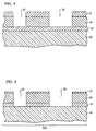
- the metallic layer 11 is then etched at its exposed portions to form a patterned metallic layer 41 (FIG. 2). More specifically, for example, the top surface of the device being manufactured is subjected to an anisotropic RIE step, using an etchant gas mixture containing oxygen and chlorine, typically in a volume ratio in the approximate range of between 0.25/1.0 and 4.0/1.0, preferably approximately 1.0/1.0. During this step the oxygen and chlorine ions are accelerated to a kinetic energy of typically about 100 eV at a gas pressure of typically about 10 Pascal and a power density of typically about 0.5 Watt/cm2. In this way, the spaces 22,32 penetrate through the chrome layer 11, where a patterned chrome layer 41 (FIG. 2) is formed. Other gases, such as nitrogen or noble gases, may be added to the etchant gas mixture for the purpose of increasing the ion flux or stabilizing the plasma, or for both purposes.
- gases such as nitrogen or noble gases, may be added to the etchant gas mixture for the purpose of increasing the ion flux or
- the patterned resist layer 12 is removed, such as by means of an oxygen plasma containing a few per centum of fluorine or of a fluorine-containing compound, as known in the art. In this way the desired photolithographic mask or reticle 300 (FIG. 3) is formed.
- an X-ray lithographic mask 500 is composed of a supporting membrane 20, an optional patterned chrome layer 51, a patterned tungsten layer 55, and a patterned chrome layer 52.
- FIG. 4 shows an earlier stage in its manufacture.
- the chrome layer 41 has been patterned in the same manner as described above, except that it now is located upon the top surface of a uniformly thick tungsten layer 55 which, in turn, has been patterned by means of RIE using a gas mixture of sulphur hexafluoride and carbon monobromotrifluoride, as known in the art, the patterned chrome layer 41 being used as a protective mask.
- the (optional) chromium layer 21 located beneath the tungsten layer 55 serves as an etch stop, for terminating the etching of tungsten, as well as a glue for promoting adherence of the tungsten layer 55 to the membrane 20.
- the chrome layer 51 is etched by means of RIE again with a gas mixture chlorine and oxygen, but without an auxiliary bombardment with oxygen.
- the chrome layer 21 is patterned to form the patterned chrome layer 51, and at the same time the thickness of the patterned chrome layer 41 is reduced, to form a patterned chrome layer 52 of reduced thickness or even zero thickness depending upon the ratio of the thicknesses of the chrome layers 21 and 41.
- the desired X-ray mask 500 is formed.
- the thickness of the chrome layer 41 is about 30 nm; of the tungsten layer 55, about 500 nm; and of the chrome layer 21, about 20 nm.
- the membrane is typically essentially silicon, silicon nitride, silicon carbide, or boron nitride, as known in the art.
- the (uniform) concentration of germanium in the aforementioned resist advantageously is the approximate range of 10 to 33 wt per centum, typically about 28 to 30 wt per centum.
- the RIE etching of the metallic layer 51 can be omitted in case optical alignment of the mask is not required.
- other metals that form refractory oxides can be added to form an organometallic resist.
- the tungsten layer 55 (FIG. 5) can be a patterned metallization or other layer in an integrated circuit or other device, with the membrane 20 replaced by an insulating layer or other component of the integrated circuit or other device that is being fabricated.
Landscapes
- Physics & Mathematics (AREA)
- General Physics & Mathematics (AREA)
- Preparing Plates And Mask In Photomechanical Process (AREA)
- Photosensitive Polymer And Photoresist Processing (AREA)
- Drying Of Semiconductors (AREA)
- Exposure Of Semiconductors, Excluding Electron Or Ion Beam Exposure (AREA)
Applications Claiming Priority (2)
| Application Number | Priority Date | Filing Date | Title |
|---|---|---|---|
| US71347991A | 1991-06-11 | 1991-06-11 | |
| US713479 | 1991-06-11 |
Publications (1)
| Publication Number | Publication Date |
|---|---|
| EP0518545A1 true EP0518545A1 (de) | 1992-12-16 |
Family
ID=24866309
Family Applications (1)
| Application Number | Title | Priority Date | Filing Date |
|---|---|---|---|
| EP92305052A Withdrawn EP0518545A1 (de) | 1991-06-11 | 1992-06-02 | Lithographisches Trockenätzverfahren mittels Gasgemischen aus Sauerstoff und Chlor |
Country Status (2)
| Country | Link |
|---|---|
| EP (1) | EP0518545A1 (de) |
| JP (1) | JP2593611B2 (de) |
Cited By (1)
| Publication number | Priority date | Publication date | Assignee | Title |
|---|---|---|---|---|
| EP0744659A1 (de) * | 1995-05-26 | 1996-11-27 | AT&T Corp. | Lithographisches Trockenätzverfahren |
Families Citing this family (5)
| Publication number | Priority date | Publication date | Assignee | Title |
|---|---|---|---|---|
| KR100701660B1 (ko) * | 2003-04-01 | 2007-03-29 | 비오이 하이디스 테크놀로지 주식회사 | 액정표시장치 제조시의 요철면 형성방법 |
| JP2006048033A (ja) * | 2004-07-09 | 2006-02-16 | Hoya Corp | フォトマスクブランク及びフォトマスクの製造方法、並びに半導体装置の製造方法 |
| KR101302630B1 (ko) * | 2004-07-09 | 2013-09-03 | 호야 가부시키가이샤 | 포토마스크 블랭크, 포토마스크 제조 방법 및 반도체장치의 제조 방법 |
| JP2007114451A (ja) * | 2005-10-20 | 2007-05-10 | Hoya Corp | マスクブランクス、および転写マスクの製造方法 |
| JP6174349B2 (ja) * | 2013-03-13 | 2017-08-02 | グンゼ株式会社 | 金属薄膜を有する無端環状樹脂フィルム |
-
1992
- 1992-04-17 JP JP12281992A patent/JP2593611B2/ja not_active Expired - Fee Related
- 1992-06-02 EP EP92305052A patent/EP0518545A1/de not_active Withdrawn
Non-Patent Citations (1)
| Title |
|---|
| WORLD PATENTS INDEX LATEST Week 8930, Derwent Publications Ltd., London, GB; AN 89-216614 & JP-A-1 154 050 (TOSHIBA K.K.) 16 June 1989 * |
Cited By (2)
| Publication number | Priority date | Publication date | Assignee | Title |
|---|---|---|---|---|
| EP0744659A1 (de) * | 1995-05-26 | 1996-11-27 | AT&T Corp. | Lithographisches Trockenätzverfahren |
| US5948570A (en) * | 1995-05-26 | 1999-09-07 | Lucent Technologies Inc. | Process for dry lithographic etching |
Also Published As
| Publication number | Publication date |
|---|---|
| JPH06250374A (ja) | 1994-09-09 |
| JP2593611B2 (ja) | 1997-03-26 |
Similar Documents
| Publication | Publication Date | Title |
|---|---|---|
| US5948570A (en) | Process for dry lithographic etching | |
| US6908716B2 (en) | Disposable hard mask for photomask plasma etching | |
| US20220367186A1 (en) | Patterning scheme to improve euv resist and hard mask selectivity | |
| US5447598A (en) | Process for forming resist mask pattern | |
| US4589952A (en) | Method of making trenches with substantially vertical sidewalls in silicon through reactive ion etching | |
| EP0489542A2 (de) | Lithographische Verfahren | |
| US6989219B2 (en) | Hardmask/barrier layer for dry etching chrome films and improving post develop resist profiles on photomasks | |
| KR20000022632A (ko) | 건식 에칭 방법 및 건식 에칭 방법을 이용한 반도체 장치의 제조방법 | |
| JP2003107675A (ja) | マスクブランク、及びマスク | |
| US4661426A (en) | Process for manufacturing metal silicide photomask | |
| US5567551A (en) | Method for preparation of mask for ion beam lithography | |
| JPH06250374A (ja) | リソグラフィーエッチング方法 | |
| JP3350095B2 (ja) | マスクの修正方法 | |
| GB2189903A (en) | An etch technique for metal mask definition | |
| US6296975B1 (en) | Photo mask of semiconductor device and method for manufacturing the same | |
| JP2909317B2 (ja) | フォトマスク | |
| JP3257130B2 (ja) | エッジ強調型位相シフトマスクの製造方法 | |
| JPS6358446A (ja) | パタ−ン形成方法 | |
| EP0268595B1 (de) | Musterübertragungsverfahren zur herstellung von halbleiteranordnungen | |
| US6150277A (en) | Method of making an oxide structure having a finely calibrated thickness | |
| JPH0363209B2 (de) | ||
| US6797638B2 (en) | Plasma-etching process for molybdenum silicon nitride layers on half-tone phase masks based on gas mixtures containing monofluoromethane and oxygen | |
| JPS6339893B2 (de) | ||
| JPH0915831A (ja) | 露光用マスクの製造方法 | |
| JP2745988B2 (ja) | フォトマスクの製造方法 |
Legal Events
| Date | Code | Title | Description |
|---|---|---|---|
| PUAI | Public reference made under article 153(3) epc to a published international application that has entered the european phase |
Free format text: ORIGINAL CODE: 0009012 |
|
| AK | Designated contracting states |
Kind code of ref document: A1 Designated state(s): DE FR GB IT |
|
| 17P | Request for examination filed |
Effective date: 19930604 |
|
| RAP3 | Party data changed (applicant data changed or rights of an application transferred) |
Owner name: AT&T CORP. |
|
| 17Q | First examination report despatched |
Effective date: 19940718 |
|
| STAA | Information on the status of an ep patent application or granted ep patent |
Free format text: STATUS: THE APPLICATION IS DEEMED TO BE WITHDRAWN |
|
| 18D | Application deemed to be withdrawn |
Effective date: 19950312 |