EP0519317B1 - Randverbinder zum Aufnehmen und Halten eines Flachkabels parallel zur Leiterplatte - Google Patents
Randverbinder zum Aufnehmen und Halten eines Flachkabels parallel zur Leiterplatte Download PDFInfo
- Publication number
- EP0519317B1 EP0519317B1 EP92109805A EP92109805A EP0519317B1 EP 0519317 B1 EP0519317 B1 EP 0519317B1 EP 92109805 A EP92109805 A EP 92109805A EP 92109805 A EP92109805 A EP 92109805A EP 0519317 B1 EP0519317 B1 EP 0519317B1
- Authority
- EP
- European Patent Office
- Prior art keywords
- housing
- tails
- terminals
- cable
- wall
- Prior art date
- Legal status (The legal status is an assumption and is not a legal conclusion. Google has not performed a legal analysis and makes no representation as to the accuracy of the status listed.)
- Expired - Lifetime
Links
- 230000037431 insertion Effects 0.000 claims description 32
- 238000003780 insertion Methods 0.000 claims description 32
- 239000004020 conductor Substances 0.000 claims description 31
- 229910000679 solder Inorganic materials 0.000 description 28
- 230000009977 dual effect Effects 0.000 description 2
- 238000005192 partition Methods 0.000 description 2
Images


Classifications
-
- H—ELECTRICITY
- H01—ELECTRIC ELEMENTS
- H01R—ELECTRICALLY-CONDUCTIVE CONNECTIONS; STRUCTURAL ASSOCIATIONS OF A PLURALITY OF MUTUALLY-INSULATED ELECTRICAL CONNECTING ELEMENTS; COUPLING DEVICES; CURRENT COLLECTORS
- H01R12/00—Structural associations of a plurality of mutually-insulated electrical connecting elements, specially adapted for printed circuits, e.g. printed circuit boards [PCB], flat or ribbon cables, or like generally planar structures, e.g. terminal strips, terminal blocks; Coupling devices specially adapted for printed circuits, flat or ribbon cables, or like generally planar structures; Terminals specially adapted for contact with, or insertion into, printed circuits, flat or ribbon cables, or like generally planar structures
- H01R12/70—Coupling devices
- H01R12/71—Coupling devices for rigid printing circuits or like structures
- H01R12/72—Coupling devices for rigid printing circuits or like structures coupling with the edge of the rigid printed circuits or like structures
-
- H—ELECTRICITY
- H01—ELECTRIC ELEMENTS
- H01R—ELECTRICALLY-CONDUCTIVE CONNECTIONS; STRUCTURAL ASSOCIATIONS OF A PLURALITY OF MUTUALLY-INSULATED ELECTRICAL CONNECTING ELEMENTS; COUPLING DEVICES; CURRENT COLLECTORS
- H01R12/00—Structural associations of a plurality of mutually-insulated electrical connecting elements, specially adapted for printed circuits, e.g. printed circuit boards [PCB], flat or ribbon cables, or like generally planar structures, e.g. terminal strips, terminal blocks; Coupling devices specially adapted for printed circuits, flat or ribbon cables, or like generally planar structures; Terminals specially adapted for contact with, or insertion into, printed circuits, flat or ribbon cables, or like generally planar structures
- H01R12/50—Fixed connections
- H01R12/51—Fixed connections for rigid printed circuits or like structures
- H01R12/55—Fixed connections for rigid printed circuits or like structures characterised by the terminals
- H01R12/58—Fixed connections for rigid printed circuits or like structures characterised by the terminals terminals for insertion into holes
-
- H—ELECTRICITY
- H01—ELECTRIC ELEMENTS
- H01R—ELECTRICALLY-CONDUCTIVE CONNECTIONS; STRUCTURAL ASSOCIATIONS OF A PLURALITY OF MUTUALLY-INSULATED ELECTRICAL CONNECTING ELEMENTS; COUPLING DEVICES; CURRENT COLLECTORS
- H01R12/00—Structural associations of a plurality of mutually-insulated electrical connecting elements, specially adapted for printed circuits, e.g. printed circuit boards [PCB], flat or ribbon cables, or like generally planar structures, e.g. terminal strips, terminal blocks; Coupling devices specially adapted for printed circuits, flat or ribbon cables, or like generally planar structures; Terminals specially adapted for contact with, or insertion into, printed circuits, flat or ribbon cables, or like generally planar structures
- H01R12/70—Coupling devices
- H01R12/71—Coupling devices for rigid printing circuits or like structures
- H01R12/72—Coupling devices for rigid printing circuits or like structures coupling with the edge of the rigid printed circuits or like structures
- H01R12/721—Coupling devices for rigid printing circuits or like structures coupling with the edge of the rigid printed circuits or like structures cooperating directly with the edge of the rigid printed circuits
-
- H—ELECTRICITY
- H01—ELECTRIC ELEMENTS
- H01R—ELECTRICALLY-CONDUCTIVE CONNECTIONS; STRUCTURAL ASSOCIATIONS OF A PLURALITY OF MUTUALLY-INSULATED ELECTRICAL CONNECTING ELEMENTS; COUPLING DEVICES; CURRENT COLLECTORS
- H01R12/00—Structural associations of a plurality of mutually-insulated electrical connecting elements, specially adapted for printed circuits, e.g. printed circuit boards [PCB], flat or ribbon cables, or like generally planar structures, e.g. terminal strips, terminal blocks; Coupling devices specially adapted for printed circuits, flat or ribbon cables, or like generally planar structures; Terminals specially adapted for contact with, or insertion into, printed circuits, flat or ribbon cables, or like generally planar structures
- H01R12/70—Coupling devices
- H01R12/77—Coupling devices for flexible printed circuits, flat or ribbon cables or like structures
- H01R12/79—Coupling devices for flexible printed circuits, flat or ribbon cables or like structures connecting to rigid printed circuits or like structures
Definitions
- the present invention relates to a printed circuit board flat flexible cable connector to contain and keep a flat flexible cable parallel to a printed circuit board, and more particularly an improvement relating to such a cable connector having a housing equipped with a plurality of terminals whose solder tails are staggered and arranged on the bottom of the housing.
- a flat, flexible cable has only one side with conductors exposed. If two cables are to be connected to a printed circuit board, normally two connectors will be necessary. For each connector, a solder tail footprint will be required. To eliminate these dual solder tail footprints, a connector has been provided which allows for the insertion of two cables with their insulated portions next to one another and their exposed portions directed outside. If this connector is designed to have this sandwiched dual cable inserted perpendicular to the printed circuit board then the solder tails may be staggered sufficiently so as to provide a small foot print.
- the foot print must be extended laterally so that the terminals do not contact one another at the bottom of the housing.
- the main object of the present invention is to solve the problems of the prior art to provide a connector to maintain either a flat, flexible cable with exposed conductors on both sides of the cable or two flat, flexible cables having only one side with exposed conductors parallel to a printed circuit board while maintaining a small solder tail foot print.
- this invention is provided which is a connector to contain and keep a flat, flexible cable, having exposed conductors on both sides, horizontal to a printed circuit board.
- the connector housing has front, rear, top and bottom walls.
- a cable insertion slot is formed in the housing front wall.
- Terminal insertion slots are in the front and rear walls of the housings.
- Lower terminals inserted in the front of the housing have a base with a length alternating between adjacent lower terminals and are held in the housing parallel to and just above the housing bottom wall.
- the lower terminals have a flexible contact arm extending into the cable insertion slot from a "C" shaped bend located at one end of the lower terminal base which is first inserted into the housing front.
- the contact points on the arms make electrical contact with the exposed conductors of the bottom portion of said flat, flexible cable.
- Tails extend from an "L” shaped bend at the end of the base opposite the "C" shaped bend, so that the tails can pass through the bottom housing wall perpendicular to the printed circuit board.
- the tails alternate passing through the housing bottom wall at different distances from the housing front wall whereby the tails form two rows parallel to the housing front and alternating in a staggered relationship.
- a plurality of upper terminals are inserted into the rear terminal insertion slots.
- the upper terminals have a base with equal lengths and are held in the housing parallel to and just below the housing top wall.
- Flexible contact arms extend into the cable insertion slot from a "C" shaped bend at one end of the upper terminal base which is first inserted into the housing rear. Contact points on the arms make electrical contact with the exposed conductors of the upper portion of the flat, flexible cable.
- Tails extend from an "L” shaped bend at the end of the base opposite the "C" shaped bend so that the tails travel down along the rear housing wall. The tails are bent a second time so that the tails travel parallel to and above the housing bottom wall and below the lower terminals.
- tails are bent a third time forming lengths between the second and third bends alternating between adjacent terminals so that the tails are not only perpendicular to the printed circuit board but also due to the alternating length of the tail formed by the third bend, the tails alternate passing through the housing bottom wall at different distances from the housing rear wall whereby the tails form two rows parallel to the housing rear wall and alternating in a staggered relationship.
- the housing also has shelves opposite the contact points partially defining the cable insertion slot to support the cable while the contact points are forced into contact with the exposed cable conductors.
- the housing bottom wall may also be separate from the housing and have holes passing therethrough in a pattern cooperating with the pattern made by the staggered tails of the terminals. After all of the terminals are inserted completely into the housing the separate bottom wall is placed over the tails and into engagement with the housing thereby holding the tails and the terminals in place in the housing.
- This connector can also be used to connect two flat cables sandwiched together with the exposed conductors facing away from each other.
- FIG. 1 is a perspective view of the flat flexible cable connector.
- FIG. 2 is a front view of the connector.
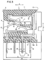
- FIG. 3 is a sectional view of the connector taken along the line 3-3 in Fig. 2.
- FIG. 4 is a sectional view of the connector taken along the line 4-4 in Fig 2.
- FIG. 5 shows schematically the staggered arrangement of the solder tails of the terminals and the holes in the bottom wall of the housing all in relation to the bottom perimeter wall of the housing.
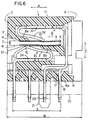
- FIG. 6 is a sectional view of the connector showing the manner in which the edge of a flat flexible cable is contained and kept horizontally to the printed circuit board.
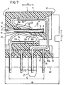
- FIG. 7 is a sectional view of the connector showing the manner in which the edges of two flat, flexible cables sandwiched together are contained and kept horizontally to the printed circuit board.
- a connector which contains and keeps a flat flexible cable horizontal to a printed circuit board.
- This connector comprises housing 1 and a plurality of terminals 2 and 32 fixed in housing 1.
- Housing 1 has a cable insertion slot 4 formed in its front 5 and extending in the front-to-rear direction A to permit insertion of a flexible cable 3 in housing 1, as seen from Fig. 6.
- the rear side of housing 1 which is the furthest from front 5 of housing 1 is indicated by 6.
- Insertion slot 4 extends lengthwise in direction B, which is perpendicular to the front-to-rear direction A, as seen from Figs. 1 and 2.
- housing 1 has terminal mounting spaces or insertion slots 7 to communicate with the cable insertion slot 4, and has partition walls 10 provided at regular intervals longitudinally as indicated by B extending from the front to back direction A. These partition walls permit lateral arrangement of terminals 30 and 31 at regular intervals and prevent direct contact between adjacent terminals.
- Upper and lower support shelves 8a and 8b are integrally connected to the upper front part and lower rear part of housing 1 respectively, extending horizontally in opposite directions in the hollow spaces 7 toward the central longitudinal line of housing 1 to permit horizontal insertion of a flexible cable 3 with conductors 9 printed on its opposite major surfaces, as seen from Fig. 6.
- FIG. 7 An alternate embodiment shown in Fig. 7 would include two cables 3', 3' back to back with exposed conductors facing opposite one another.
- Upper terminal 31 is fixed in the housing 1 so that it may be put in contact with a selected conductor 9 on the upper major surface 12 of the cable 3 when the upper terminal is inserted in the rear 6 of the housing 1 whereas lower terminal 30 is fixed so that it may be put in contact with a selected conductor 9 on the lower major surface 14 of cable 3 when the lower terminal is inserted in the front 5 of the housing 1.
- each upper terminal 31 consists of a base 33 with contact beam or arm 32 and solder tail 18 both integrally connected.
- Contact beam 32 extends from the base 33 from a C shaped bend into the cable insertion slot 4 and ends with contact point 13.
- Each contact point 13 is adapted to be put in contact with a selected conductor 9 on upper major surface 12 of printed board 3.
- Each contact point 13 is opposite a portion of the lower support shelf 8b which provides a resilient force to push the lower side of the cable so that a selected conductor in the upper major surface 14 makes contact with the selected contact point 13.
- each lower terminal 30 consists of a base 34 with a contact beam or arm 2 and solder tail 18 both integrally connected.
- Contact beam 2 extends from base 34 from a "C" shaped bend into the cable insertion slot 4 and again turns at contact point 15 and extends downward.
- Each contact point 15 is adapted to be put in contact with a selected conductor 9 on the lower major surface 14 of the printed board 3.
- Each contact point 15 is opposite a portion of the upper support shelve 8a which provides a resilient force to push the upper side of the cable so that a selected conductor in the cable lower major surface 14 makes contact with the selected contact point 15.
- Housing 1 has a plurality of holes 17 on its floor 16, thereby permitting the solder tail 18 of each terminal 30 and 31 to pass through floor 16 of housing 1 and partly appear from the bottom of housing 1.
- These holes 17 are staggered and arranged on the bottom of housing 1 so as to form four parallel lines, and accordingly projecting solder tails 18 are staggered and arranged on the bottom of housing 1 in four parallel lines, as seen from Fig. 5.
- a pair of opposing terminals 30 and 31 which are crossed by the line 3-3 in Fig. 2 appear in complete form in Fig. 3.
- the solder tail 18 of the lower terminal 30 being on the first line and the solder tail 18 of upper terminal 31 being on the third line.
- Another pair of terminals 30, 31 which are crossed by the line 4-4 in Fig. 2 appear partly in Fig. 3. Specifically only their solder tails 18 appear.
- the solder tail 18 of the front terminal 30 is on the second line and the solder tail 18 of the rear terminal 31 is on the fourth line.
- all solder tails 18 project downwards from the bottom of housing 1, not extending laterally out of the area bounded by the four sides of the square housing bottom.
- terminals 30 and 31 are fixed in the housing 1 so that the contact portions 13, 15 of the contact beams may be positioned above the bottom floor of housing within the lateral range of the farthest distance S from the first line of solder tails closest to insertion slot 4 to the fourth line of solder tails closest to the rear side of housing 1.
- contact portion 15 of lower terminal 30 whose solder tail 18 is in the first line is just above the second line of the staggered pattern
- the contact portion 13 of upper terminal counter-contact 31 whose solder tail 18 is in the third line is just between the second and third lines of the staggered pattern, as seen from Fig. 3.
- the distance L from the tip 19 of the lower terminal 30 which is closest to insertion slot 4 to the rear extension 24 of the upper terminal 31 which is closest to rear wall 6 need not be increased, and hence the lateral size W of housing 1 need not be increased, either.
- the staggering of the upper terminal 31 solder tails 18 is a result of the alternating length of the adjacent solder tail portions just above and parallel to the housing bottom. These solder tail portions are also below the bases 34 of the lower terminals.
- Housing 1 has two split projections 21 on opposite bottom ends, thus permitting the mounting of housing 1 on a, printed board 20.
- each split projection 21 has a longitudinal slot 23 and an annular projection 22 to be resiliently fitted in and caught by a corresponding hole, which is made in a printed board.
- a flexible cable 3 is inserted in insertion slot 4.
- lower terminal beam 2 is yieldingly bent downwards, thereby resiliently pushing itself against selected conductor 9 on the lower surface 14 of cable 3
- upper terminal beam 32 is yieldingly bent upwards, thereby resiliently pushing itself against selected conductor 9 on the upper surface 12 of cable 3.
- flexible cable 3 is supported by upper and lower support shelves 8a and 8b, thus putting cable 3 in correct vertical position in the direction indicated by C.
- reliable electric contacts are made between upper and lower terminals and conductors 9 on opposite major surfaces 12 and 14 of printed board 3.
- split projections 21 of housing 1 are pushed in the corresponding holes of a printed board 20.
- Each split projection 21 reduces its diameter when passing through an associated hole, and as seen from Fig. 6, it returns to its original size when annular projection 22 appears from printed board 20, allowing annular projection 22 to expand, thus being caught by the circumference of the hole in locking condition.
- the cable connector is fixed to printed board 20.
- Selected conductors on printed board 20 can be soldered to solder tails 18 of board edge connector, thereby making necessary electric connections between selected conductors of flexible printed board 3 and those of printed board 20 via the connector terminals.
Landscapes
- Coupling Device And Connection With Printed Circuit (AREA)
- Multi-Conductor Connections (AREA)
- Manufacturing Of Electrical Connectors (AREA)
Claims (6)
- Verbinder (1) zur Herstellung eines elektrischen Kontaktes zwischen freiliegenden Adern (9) eines flachen, biegsamen Kabels (3) und einer Druckschaltungsplatte sowie einer Halterung des Kabels parallel zu der Druckschaltungsplatte mit:einem Gehäuse mit einer Vorderwand (5), einer Rückwand (6), einer oberen Wand (11) und einer Bodenwand (6),einem Kabeleinführungsschlitz (4), der in der Vorderwand (5) des Gehäuses angebracht ist und in den das Kabel eingeführt wird,eine Vielzahl von Anschlußeinführungsschlitzen (7) in der Vorder- und der Rückwand des Gehäuses,eine Vielzahl von unteren Anschlüssen (30), die in die vorderen Anschlußeinführungsschlitze (7) eingesetzt sind,wobei die unteren Anschlüsse (30) eine Basis (34) besitzen, deren Länge zwischen benachbarten unteren Anschlüssen abwechselt,die Basis (34) der unteren Anschlüsse im Gehäuse parallel und dicht oberhalb der Bodenwand (16) angeordnet sind und biegsame Kontaktarme (2) besitzen, die sich von einer C-förmigen Biegung an einem Ende der Basis (34) des vorderen Anschlusses in den Kabeleinführungsschlitz (4) erstrecken, wobei die Basis als erstes in die Vorderwand (5) des Gehäuses eingeführt wird, die Arme elektrischen Kontakt an Kontaktpunkten (15) mit den freiliegenden Adern (9) des unteren Teils (14) des flachen, biegsamen Kabels (3) machen, und Schwänze (18) sich von einer L-förmigen Biegung am Ende der Basis und gegenüber der C-förmigen Biegung erstrecken, so daß die Schwänze (18) sich durch die Bodenwand (16) des Gehäuses rechtwinklig zur Druckschaltungsplatte (20) erstrecken, wobei aufgrund der abwechselnden Länge der Basis (34) der unteren Anschlüsse die Schwänze (18) abwechselnd durch die Bodenwand (16) des Gehäuses in unterschiedlichen Abständen von der Vorderwand (5) des Gehäuses führen, wodurch die Schwänze (18) zwei Reihen bilden, die parallel zur Vorderseite des Gehäuses und abwechselnd in einer versetzten Beziehung verlaufen, undmit einer Vielzahl von oberen Anschlüssen (31), die in die rückwärtigen Anschlußeinführungsschlitze (7) eingesetzt sind, wobeidie oberen Anschlüssen (31) je eine Basis (33) mit gleicher Länge besitzen,die Basis (33) der oberen Anschlüsse, die im Gehäuse parallel zu und dicht unterhalb der oberen Wand (11) des Gehäuses gehalten werden, einen biegsamen Kontaktarm (32) besitzen, der sich von einer C-förmigen Biegung an einem Ende der als erstes in die Rückwand (6) des Gehäuses eingesetzten Basis (33) der oberen Anschlüsse aus in den Kabeleinführungsschlitz (4) erstreckt, die Arme (32) elektrischen Kontakt an Kontaktpunkten (13) mit den freiliegenden Adern (9) des oberen Teils (12) des flachen, biegsamen Kabels (3) machen, und mit Schwänzen (18), die sich von einer L-förmigen Biegung am Ende der Basis (33) und gegenüberliegend der C-förmigen Biegung erstrecken, so daß sie entlang der Rückwand (6) des Gehäuses nach unten führen, wobei die Schwänze ein zweites Mal abgebogen sind, so daß sie parallel zu und oberhalb der Bodenwand (16) des Gehäuses verlaufen und ein drittes Mal unter Bildung von Abschnitten abgebogen sind, deren Länge zwischen der zweiten und dritten Biegung benachbarter Anschlüsse abwechselt, so daß die Schwänze (18) rechtwinklig zu der Druckschaltungsplatte verlaufen, wobei aufgrund der abwechselnden Länge des durch die dritte Biegung gebildeten Schwanzabschnitts, die Schwänze abwechselnd durch die Bodenwand (16) des Gehäuses im abwechselnden Abständen von der Gehäuserückwand führen, wodurch die Schwänze zwei Reihen bilden, die parallel zur Gehäuserückwand (6) und abwechselnd in versetzter Beziehung verlaufen.
- Verbinder nach Anspruch 1, bei dem das Gehäuse gegenüber den Kontaktpunkten (15, 13) Sockel (8a, 8b) aufweist, die den Kabeleinführungsschlitz (4) teilweise definieren, um das Kabel (3) zu stützen, während die Kontaktpunkte (15, 13) in Kontakt mit den freiliegenden Kabeladern (9) gebracht werden.
- Verbinder nach Anspruch 2, bei dem die Gehäusebodenwand (16a) getrennt vom Gehäuse ist und Öffnungen (17) besitzt, die durch die Bodenwand mit einem Muster führen, das mit dem durch die versetzten Schwänze (18) der Anschlüsse (30, 31) zusammenwirkt, wodurch nach vollständigem Einsetzen aller Anschlüsse in das Gehäuse die getrennte Bodenwand (16a) über die Schwänze (18) und in Verbindung mit dem die Schwänze (18) haltenden Gehäuse und den Anschlüssen (30, 31) im Gehäuse gebracht wird.
- Verbinder (1) zur Herstellung eines elektrischen Kontaktes zwischen den freiliegenden Adern (9) von zwei flachen, biegsamen Kabeln (3), die Sandwich-artig zusammengebracht sind, wobei die freiliegenden Adern (9) voneinander weg weisen, zu einer Druckschaltungsplatte und zur Halterung des Kabels parallel zu der Druckschaltungsplatte, mit:einem Gehäuse, das eine Vorderwand (5), eine Rückwand (6), eine obere Wand (11) und eine Bodenwand (16) aufweist,einem Kabeleinführungsschlitz (4), der in der Gehäusevorderwand (5) angebracht ist und in den das Kabel eingeführt wird,eine Vielzahl von Anschlußeinführungsschlitzen (7) in der Vorder- und Rückwand des Gehäuses,eine Vielzahl von unteren Anschlüssen (30), die in die vorderen Anschlußeinführungsschlitze (7) eingesetzt sind, wobeidie unteren Anschlüsse (30) eine Basis (34) besitzen, deren Länge zwischen benachbarten unteren Anschlüssen abwechselt,die Basis (34) der unteren Anschlüsse im Gehäuse parallel zu und dicht oberhalb der Gehäusebodenwand (16) gehalten werden und biegsame Kontaktarme (2) aufweisen, die sich ausgehend von einer C-förmigen Biegung an einem Ende der als erstes in die Gehäusevorderwand (5) eingesetzten Basis (34) der unteren Anschlüsse in den Kabeleinführungsschlitz (4) erstrecken, die Arme elektrischen Kontakt an Kontaktpunkten (15) mit den freiliegenden Adern (9) des unteren, flachen und biegsamen Kabels machen, und Schwänze (18) sich von einer L-förmigen Biegung an dem der C-förmigen Biegung gegenüberliegenden Ende der Basis (34) ausgehen, so daß die Schwänze (18) durch die Gehäusebodenwand (16) rechtwinklig zur Druckschaltungsplatte (20) verlaufen, wobei aufgrund der abwechselnden Länge der Basis (34) der unteren Anschlüsse die Schwänze (18) abwechseln in unterschiedlichen Abständen von der Gehäusevorderwand (5) durch die Gehäusebodenwand (16) führen, wodurch die Schwänze (18) zwei Reihen bilden, die parallel zur Gehäusevorderwand und abwechselnd in einer versetzten Beziehung verlaufen, und wobeieine Vielzahl von oberen Anschlüssen (31) in die rückwärtigen Anschlußeinführungsschlitze (7) eingesetzt sind,die oberen Anschlüsse (31) eine Basis (33) mit gleicher Länge besitzen,die Basis (33) der oberen Anschlüsse im Gehäuse parallel zu und dicht unterhalb der oberen Gehäusewand (11) gehalten werden und einen biegsamen Kontaktarm (32) besitzen, der sich ausgehend von einer C-förmigen Biegung an einem Ende der als erstes in die Gehäuserückwand (6) eingeführten Basis (33) der rückwärtigen Anschlüssen in den Kabeleinführungsschlitz (4) erstreckt, wobei die Arme (32) elektrischen Kontakt an Kontaktpunkten (13) mit den freiliegenden Adern (9) des oberen, flachen und biegsamen Kabels machen, und Schwänze (18) sich ausgehend von einer L-förmigen Biegung an dem der C-förmigen Biegung gegenüberliegenden Ende der Basis (33) erstrecken, so daß die Schwänze entlang der Gehäuserückwand (6) nach unten verlaufen und ein zweites Mal abgebogen sind, so daß die Schwänze parallel zu und oberhalb der Gehäusebodenwand (16) entlanglaufen, sowie ein drittes Mal gebogen sind und Abschnitte zwischen der zweiten und dritten Biegung bilden, deren Länge zwischen benachbarten Anschlüssen abwechselt, so daß die Schwänze (18) rechtwinklig zu der Druckschaltungsplatte verlaufen, wobei aufgrund der abwechselnden Länge der durch die dritte Biegung gebildeten Schwanzabschnitte die Schwänze abwechseln in unterschiedlichen Abständen von der Gehäuserückwand (6) durch die Gehäusebodenwand (16) führen, wodurch die Schwänze (18) zwei Reihen bilden, die parallel zu der Gehäuserückwand (6) und abwechselnd in versetzter Beziehung verlaufen.
- Verbinder nach Anspruch 4, bei dem das Gehäuse gegenüberliegend von den Kontaktpunkten (15, 13) Sockel (89, 86) besitzt, die den Kabeleinführungsschlitz (4) teilweise definieren, um die Kabel (3') zu stützen, während die Kontaktpunkte (15, 13) in Kontakt mit den freiliegenden Kabeladern (9) gebracht werden.
- Verbinder nach Anspruch 5, bei dem die Gehäusebodenwand (16a) getrennt von dem Gehäuse ist und Öffnungen (17) aufweist, die durch die Bodenwand in einem mit dem Muster der versetzten Schwänze (18) der Anschlüsse (30, 31) zusammenwirkenden Muster verlaufen, wodurch nach vollständigem Einsetzen aller Anschlüsse in das Gehäuse die getrennte Bodenwand (16a) über den Schwänzen (18) und in Verbindung mit dem die Schwänze (18) haltenden Gehäuse und den Anschlüssen (30, 31) im Gehäuse gebracht wird.
Applications Claiming Priority (2)
| Application Number | Priority Date | Filing Date | Title |
|---|---|---|---|
| JP3173243A JPH069152B2 (ja) | 1991-06-18 | 1991-06-18 | 水平基板接続用カードエッヂコネクタ及びその製法 |
| JP173243/91 | 1991-06-18 |
Publications (3)
| Publication Number | Publication Date |
|---|---|
| EP0519317A2 EP0519317A2 (de) | 1992-12-23 |
| EP0519317A3 EP0519317A3 (en) | 1993-06-16 |
| EP0519317B1 true EP0519317B1 (de) | 1996-03-06 |
Family
ID=15956816
Family Applications (1)
| Application Number | Title | Priority Date | Filing Date |
|---|---|---|---|
| EP92109805A Expired - Lifetime EP0519317B1 (de) | 1991-06-18 | 1992-06-11 | Randverbinder zum Aufnehmen und Halten eines Flachkabels parallel zur Leiterplatte |
Country Status (5)
| Country | Link |
|---|---|
| US (1) | US5201661A (de) |
| EP (1) | EP0519317B1 (de) |
| JP (1) | JPH069152B2 (de) |
| KR (1) | KR950012475B1 (de) |
| DE (1) | DE69208744T2 (de) |
Families Citing this family (30)
| Publication number | Priority date | Publication date | Assignee | Title |
|---|---|---|---|---|
| JP3225065B2 (ja) * | 1991-09-17 | 2001-11-05 | ケル株式会社 | 電気コネクタ |
| WO1993018559A1 (en) * | 1992-03-06 | 1993-09-16 | Augat Inc. | Edge card interconnection system |
| US5503564A (en) * | 1992-10-30 | 1996-04-02 | The Whitaker Corporation | Assembly of an electrical connector and ejector unit for connecting IC cards to printed circuit boards |
| JP2561501Y2 (ja) * | 1992-12-25 | 1998-01-28 | モレックス インコーポレーテッド | フレキシブルプリント回路基板接続用の電気コネクタ |
| JP2575272Y2 (ja) * | 1993-01-27 | 1998-06-25 | 日本エー・エム・ピー株式会社 | 平形ケーブル用コネクタ |
| JP2822852B2 (ja) * | 1993-06-30 | 1998-11-11 | 住友電装株式会社 | カードエッジコネクタ |
| US5827075A (en) * | 1993-09-08 | 1998-10-27 | The Whitaker Corporation | Assembly of an electrical connector and ejector unit for connecting IC cards to printed circuit boards |
| USD362658S (en) | 1994-09-28 | 1995-09-26 | Motorola, Inc. | Electric connector |
| CA2158703A1 (en) * | 1994-09-30 | 1996-03-31 | Kevin G. Henderson | Electrical connector and alignment apparatus for contact pins thereof |
| US5609491A (en) * | 1995-03-10 | 1997-03-11 | The Whitaker Corporation | Electrical connector for printed circuit board assembly |
| JP3019288U (ja) * | 1995-06-08 | 1995-12-12 | モレックス インコーポレーテッド | 平型柔軟ケーブル用電気コネクタ |
| JP3104600B2 (ja) * | 1995-12-19 | 2000-10-30 | 住友電装株式会社 | フラットケーブル用コネクタ |
| US5791925A (en) * | 1996-06-28 | 1998-08-11 | Berg Technology, Inc. | Card edge connector |
| JPH1022009A (ja) * | 1996-07-05 | 1998-01-23 | Amp Japan Ltd | フラットケーブル用コネクタ |
| JP3424150B2 (ja) * | 1996-12-27 | 2003-07-07 | モレックス インコーポレーテッド | 電気コネクタ |
| US6000951A (en) * | 1997-03-18 | 1999-12-14 | Prince Corporation | Electrical ribbon wire connectors |
| JP3903332B2 (ja) * | 1998-06-12 | 2007-04-11 | モレックス インコーポレーテッド | 電気コネクタ |
| US6089925A (en) * | 1998-10-06 | 2000-07-18 | The Whitaker Corporation | Modular electrical connector having electrical contact modules |
| US6155876A (en) * | 1998-12-23 | 2000-12-05 | Hon Hai Precision Ind. Co., Ltd. | Connector adapter |
| USD456407S1 (en) | 1999-12-29 | 2002-04-30 | Tyco Electronics Logistics Ag | Stacked smart card reader |
| USD454875S1 (en) | 1999-12-29 | 2002-03-26 | Tyco Electronics Logistics Ag | Single smart card reader |
| US6508673B2 (en) | 2000-04-05 | 2003-01-21 | Mcdowell Jennifer Lyn | Low cost smart card reader, extension style, with wiping contacts |
| US6257926B1 (en) * | 2000-06-21 | 2001-07-10 | Hon Hai Precision Ind. Co., Ltd. | Guiding post with press-fit arrangement |
| US6383010B1 (en) * | 2001-04-23 | 2002-05-07 | Molex Incorporated | Latching system for electrical connectors |
| USD455127S1 (en) | 2001-06-26 | 2002-04-02 | Hon Hai Precision Ind. Co., Ltd. | Electrical connector |
| TW572395U (en) * | 2002-01-23 | 2004-01-11 | Hon Hai Prec Ind Co Ltd | Electrical connector assembly |
| TW539306U (en) * | 2002-06-20 | 2003-06-21 | Hon Hai Prec Ind Co Ltd | Electrical connector |
| JP2007218967A (ja) * | 2006-02-14 | 2007-08-30 | Matsushita Electric Ind Co Ltd | プラズマディスプレイ装置 |
| CN104904070B (zh) * | 2012-12-11 | 2018-11-13 | 诺基亚技术有限公司 | 提供用于接触柔性平坦连接件的插座触点的装置和方法 |
| JP6293634B2 (ja) * | 2014-10-03 | 2018-03-14 | 日本航空電子工業株式会社 | コネクタ |
Family Cites Families (13)
| Publication number | Priority date | Publication date | Assignee | Title |
|---|---|---|---|---|
| US3696319A (en) * | 1970-08-20 | 1972-10-03 | Berg Electronics Inc | Flat conductor cable connector |
| JPS5696474A (en) * | 1979-12-28 | 1981-08-04 | Sumitomo Electric Industries | Connector |
| US4298237A (en) * | 1979-12-20 | 1981-11-03 | Bell Telephone Laboratories, Incorporated | Printed wiring board interconnection apparatus |
| US4367006A (en) * | 1980-12-10 | 1983-01-04 | Amp Incorporated | Connector for flat cable |
| US4514030A (en) * | 1981-08-27 | 1985-04-30 | Methode Electronics, Inc. | Shorting edge connector |
| GB2105118B (en) * | 1981-08-27 | 1985-04-03 | Methode Electronics Inc | Electrical edge connector |
| US4842538A (en) * | 1983-11-23 | 1989-06-27 | Burndy Corporation | Low insertion force circuit board connector assembly |
| US4636021A (en) * | 1984-03-02 | 1987-01-13 | Amp Incorporated | High density ZIF card edge connector |
| US4780095A (en) * | 1987-03-17 | 1988-10-25 | Digital Equipment Corporation | Edge connector for circuit boards |
| DE3854593T2 (de) * | 1987-08-19 | 1996-04-18 | Japan Aviation Electron | Elektrische Steckverbindung, am Kabelende angeschlossen und ausgestattet mit Mitteln zur Verringerung der Zugkraft, die auf das Kabel und durch das Kabel wirkt. |
| US4869672A (en) * | 1989-04-17 | 1989-09-26 | Amp Incorporated | Dual purpose card edge connector |
| US4913656A (en) * | 1989-04-07 | 1990-04-03 | Rogers Corporation | Electrical connector |
| US5071371A (en) * | 1990-03-30 | 1991-12-10 | Molex Incorporated | Electrical card edge connector assembly |
-
1991
- 1991-06-18 JP JP3173243A patent/JPH069152B2/ja not_active Expired - Lifetime
-
1992
- 1992-05-13 US US07/882,333 patent/US5201661A/en not_active Expired - Fee Related
- 1992-06-11 EP EP92109805A patent/EP0519317B1/de not_active Expired - Lifetime
- 1992-06-11 DE DE69208744T patent/DE69208744T2/de not_active Expired - Fee Related
- 1992-06-17 KR KR1019920010483A patent/KR950012475B1/ko not_active Expired - Fee Related
Also Published As
| Publication number | Publication date |
|---|---|
| EP0519317A3 (en) | 1993-06-16 |
| EP0519317A2 (de) | 1992-12-23 |
| KR950012475B1 (ko) | 1995-10-18 |
| DE69208744D1 (de) | 1996-04-11 |
| JPH069152B2 (ja) | 1994-02-02 |
| JPH04370678A (ja) | 1992-12-24 |
| KR930001513A (ko) | 1993-01-16 |
| US5201661A (en) | 1993-04-13 |
| DE69208744T2 (de) | 1996-07-25 |
Similar Documents
| Publication | Publication Date | Title |
|---|---|---|
| EP0519317B1 (de) | Randverbinder zum Aufnehmen und Halten eines Flachkabels parallel zur Leiterplatte | |
| US5460546A (en) | Electric connector terminal and method of marking the same | |
| US5161987A (en) | Connector with one piece ground bus | |
| JP2649759B2 (ja) | 印刷回路板に取り付ける電気コネクタ | |
| EP0922318B1 (de) | Leiterplattenmontierbarer elektrischer verbinder | |
| EP0347097B1 (de) | Elektrisches Verbindersystem | |
| US5695354A (en) | Printed circuit board connector | |
| US4708415A (en) | Electrical connectors | |
| EP0104013A1 (de) | Elektrischer Vielfachsteckverbinder | |
| US4655522A (en) | Electrical terminal receptacle | |
| EP0448382B1 (de) | Kontaktbüchse für einen elektrischen Verbinder | |
| US3320572A (en) | Electrical connector assembly | |
| EP0554003B1 (de) | Beidseitig ausgestattete Verlängerungsfassung für Ausleseplatinen | |
| US6293805B1 (en) | Board to board connector | |
| EP0242019A2 (de) | Nachrichtenverbindungsstecker | |
| EP0304079B1 (de) | Elektrische Steckverbindung, am Kabelende angeschlossen und ausgestattet mit Mitteln zur Verringerung der Zugkraft, die auf das Kabel und durch das Kabel wirkt | |
| EP0191539A2 (de) | Elektrisches Anschlussendstück für Steckverbinder | |
| US5919064A (en) | Card edge connector with similar shaped cantilevered beam spring contacts having multi-level contact areas | |
| US4545634A (en) | Multi-contact connector | |
| US5931701A (en) | Electrical connector assembly | |
| US6019633A (en) | Electronic card connector | |
| EP0358404B1 (de) | Verbinder | |
| JPH0630266B2 (ja) | 低挿入力の電気コネクタ | |
| US6042397A (en) | Board-mounted connector | |
| EP1063726A2 (de) | Elektrischer Steckverbinder mit mehrfachen Kontakten |
Legal Events
| Date | Code | Title | Description |
|---|---|---|---|
| PUAI | Public reference made under article 153(3) epc to a published international application that has entered the european phase |
Free format text: ORIGINAL CODE: 0009012 |
|
| AK | Designated contracting states |
Kind code of ref document: A2 Designated state(s): DE FR GB IT |
|
| PUAL | Search report despatched |
Free format text: ORIGINAL CODE: 0009013 |
|
| AK | Designated contracting states |
Kind code of ref document: A3 Designated state(s): DE FR GB IT |
|
| 17P | Request for examination filed |
Effective date: 19931008 |
|
| 17Q | First examination report despatched |
Effective date: 19950405 |
|
| ITF | It: translation for a ep patent filed | ||
| GRAA | (expected) grant |
Free format text: ORIGINAL CODE: 0009210 |
|
| AK | Designated contracting states |
Kind code of ref document: B1 Designated state(s): DE FR GB IT |
|
| REF | Corresponds to: |
Ref document number: 69208744 Country of ref document: DE Date of ref document: 19960411 |
|
| ET | Fr: translation filed | ||
| PLBE | No opposition filed within time limit |
Free format text: ORIGINAL CODE: 0009261 |
|
| STAA | Information on the status of an ep patent application or granted ep patent |
Free format text: STATUS: NO OPPOSITION FILED WITHIN TIME LIMIT |
|
| 26N | No opposition filed | ||
| PGFP | Annual fee paid to national office [announced via postgrant information from national office to epo] |
Ref country code: GB Payment date: 20010502 Year of fee payment: 10 |
|
| PGFP | Annual fee paid to national office [announced via postgrant information from national office to epo] |
Ref country code: FR Payment date: 20010531 Year of fee payment: 10 |
|
| PGFP | Annual fee paid to national office [announced via postgrant information from national office to epo] |
Ref country code: DE Payment date: 20010627 Year of fee payment: 10 |
|
| REG | Reference to a national code |
Ref country code: GB Ref legal event code: IF02 |
|
| PG25 | Lapsed in a contracting state [announced via postgrant information from national office to epo] |
Ref country code: GB Free format text: LAPSE BECAUSE OF NON-PAYMENT OF DUE FEES Effective date: 20020611 |
|
| PG25 | Lapsed in a contracting state [announced via postgrant information from national office to epo] |
Ref country code: DE Free format text: LAPSE BECAUSE OF NON-PAYMENT OF DUE FEES Effective date: 20030101 |
|
| GBPC | Gb: european patent ceased through non-payment of renewal fee |
Effective date: 20020611 |
|
| PG25 | Lapsed in a contracting state [announced via postgrant information from national office to epo] |
Ref country code: FR Free format text: LAPSE BECAUSE OF NON-PAYMENT OF DUE FEES Effective date: 20030228 |
|
| REG | Reference to a national code |
Ref country code: FR Ref legal event code: ST |
|
| PG25 | Lapsed in a contracting state [announced via postgrant information from national office to epo] |
Ref country code: IT Free format text: LAPSE BECAUSE OF NON-PAYMENT OF DUE FEES;WARNING: LAPSES OF ITALIAN PATENTS WITH EFFECTIVE DATE BEFORE 2007 MAY HAVE OCCURRED AT ANY TIME BEFORE 2007. THE CORRECT EFFECTIVE DATE MAY BE DIFFERENT FROM THE ONE RECORDED. Effective date: 20050611 |