EP0520572A1 - Informationsverarbeitungsvorrichtung - Google Patents
Informationsverarbeitungsvorrichtung Download PDFInfo
- Publication number
- EP0520572A1 EP0520572A1 EP92201842A EP92201842A EP0520572A1 EP 0520572 A1 EP0520572 A1 EP 0520572A1 EP 92201842 A EP92201842 A EP 92201842A EP 92201842 A EP92201842 A EP 92201842A EP 0520572 A1 EP0520572 A1 EP 0520572A1
- Authority
- EP
- European Patent Office
- Prior art keywords
- memory
- box
- unit
- instruction
- data
- Prior art date
- Legal status (The legal status is an assumption and is not a legal conclusion. Google has not performed a legal analysis and makes no representation as to the accuracy of the status listed.)
- Granted
Links
Images


Classifications
-
- G—PHYSICS
- G06—COMPUTING OR CALCULATING; COUNTING
- G06F—ELECTRIC DIGITAL DATA PROCESSING
- G06F9/00—Arrangements for program control, e.g. control units
- G06F9/06—Arrangements for program control, e.g. control units using stored programs, i.e. using an internal store of processing equipment to receive or retain programs
- G06F9/30—Arrangements for executing machine instructions, e.g. instruction decode
- G06F9/38—Concurrent instruction execution, e.g. pipeline or look ahead
- G06F9/3885—Concurrent instruction execution, e.g. pipeline or look ahead using a plurality of independent parallel functional units
-
- G—PHYSICS
- G06—COMPUTING OR CALCULATING; COUNTING
- G06F—ELECTRIC DIGITAL DATA PROCESSING
- G06F9/00—Arrangements for program control, e.g. control units
- G06F9/06—Arrangements for program control, e.g. control units using stored programs, i.e. using an internal store of processing equipment to receive or retain programs
- G06F9/30—Arrangements for executing machine instructions, e.g. instruction decode
-
- G—PHYSICS
- G06—COMPUTING OR CALCULATING; COUNTING
- G06F—ELECTRIC DIGITAL DATA PROCESSING
- G06F9/00—Arrangements for program control, e.g. control units
- G06F9/06—Arrangements for program control, e.g. control units using stored programs, i.e. using an internal store of processing equipment to receive or retain programs
- G06F9/30—Arrangements for executing machine instructions, e.g. instruction decode
- G06F9/38—Concurrent instruction execution, e.g. pipeline or look ahead
Definitions
- the operating units of microcomputers of the PC type can be formed of a first operating member constituted by an arithmetic and logical unit and by a second member constituted by a mathematical coprocessor dedicated to floating calculation operations.
- a first operating member constituted by an arithmetic and logical unit
- a second member constituted by a mathematical coprocessor dedicated to floating calculation operations.
- the object of the invention is to provide a device, of the type mentioned in the preamble, which is formed by an operating unit which can have a complex structure and which can be composed of a plurality of operating members and for which coordination and asynchronism issues are largely resolved.
- the operating unit can include at least one FIFO type memory device connected between the operating devices and the central instruction decoding unit, one or more executing devices that can operate in parallel under the control of a single decoding unit d 'instructions.
- the invention is particularly suitable for processors designed to process chained languages of the FORTH type for example.
- European patent application No. 0 185 215 or better the patent application filed simultaneously in France with the present application under No. 91 08062.
- coordination problems are still lightened because an asynchronous type of operation is envisaged between the different components of the device.
- an information processing device is remarkable in that it comprises at least one memory for return of call of procedure call of the stack type and at least one data memory. also battery-type intermediates.
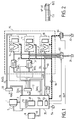
- Figure 1 shows a block diagram of a device according to the invention.
- FIG. 2 shows the format of the instructions.
- Figure 3 shows the structure of a central decoding unit.
- Figure 4 shows the structure of the operating bodies.
- Figure 5 shows the structure of a memory organ.
- Figures 6, 7, 8 show a flow diagram defining the operation of the central operating unit.
- FIG. 9 represents a flow chart defining the operation of the operating unit.
- Figure 1 there is shown an information processing device, more particularly adapted to programs written in FORTH.
- the program information formed of instructions and parameters is stored in a program memory 1. This information appears at the output 3 of this memory 1.
- the address code where this program information is stored is applied to the input address 5 of this memory 1.
- a memory 8 of the “LIFO” stack type hereinafter called return memory, is provided to contain address codes for memory 1. These address codes indicate the location, in memory 1, of the instruction to be executed after the execution of a subroutine. The address codes of this stack memory 8 are available on an access 10.
- the execution of the instructions with, optionally, the processing of different parameters takes place in an operation unit 15 formed of three operating organs 16, 17 and 18. These organs essentially comprise on the one hand an arithmetic and logic unit ALU 20, 21 and 22 respectively having various possibilities, for example the multiplication can be wired for one and not for the other.
- these units include a stack memory 25, 26 and 27 respectively to contain various data, partial results, etc.
- the processing device communicates with the outside world by means of two ports 29 and 30, port 29 for the input of information and port 30 for the output.
- a central decoding unit 35 determines the different routes of information between the memories 1 and 8, the operation unit 15 and the ports 29 and 30.
- the operation unit 15 comprises two memory bodies 36 and 37 formed from memories of the FIFO type; these organs are connected between the unit 35 and the operating members 16 and 17 respectively.
- the operating unit 18 is, for its part, connected directly to the unit 35; a common data line 46 provides the link between the members 36, 37, the unit 18 and the central decoding unit 35.
- the central decoding unit 35 comprises a decoding member 48 constituted advantageously, from an associative memory with its input register 49, an addressing register 50 for addressing the program memory 1 also called register program, an interrupt management unit 52 which manages the interrupts triggered by signals applied to the input 54 of the unit 35, and a sequencing unit 60 which manages the operation thereof.
- This unit 35 includes other elements which will be explained later in the present description.
- the information coming from the terminal 29 can be directed to one of the members 16, 17 or 18 by acting on a switch 62.
- the information to be supplied to the output terminal 30 they are stored in a buffer register 64, the loading command of which comes from the unit 35.
- the inputs of this buffer register are connected to a common data line (BUS line) 66.
- This data output line 66 interconnects unit 35 with all units 16, 17 to 18.
- the unit 35 requests the reading of data contained in one of the battery memories 25, 26 or 27.
- the data is available and ready when a RAD signal becomes active.
- This signal is produced in the following manner from the DLVi and RADi signals.
- DLVi signals mean that the unit 35 requests the reading of the memory 25, 26 and 27 concerned.
- RAF (DAV1.RAF1) + (DAV2.RAF2) + (DAV3.RAF3) if it is only possible to solicit one organ at a time.
- the RAF signal must be active when all the organs have responded, which makes it possible to write simultaneously to several organs 16 to 18.
- the signal RAF3 merges with the signal DL emanating from the unit 18 and the signal DAV3 with a signal LA to be applied to this same member 18.
- These signals DL and LA will be explained below.
- FIG. 3 shows in detail the central processing unit 35.
- the address register 50 can be loaded in different ways, depending on the positions of a switching circuit 95. In a first position, its content is incremented by one by means of an incrementer 97. In a second position , it is loaded by the output information of the stack memory 8 via a switch 98. In a third position, it is loaded from a circuit 52, by the address of the interrupt program and, in a fourth position by the content of the data of the program memory 1 via the switch 90.
- register 105 coupled to a decoder 107 to provide a TEST signal.
- This register can be loaded by information coming from the associative memory 48 or by information conveyed by the line 66.
- This register 105 is connected to the line 66 by a switch 108 controlled by the signal CMI.
- FIG. 4 shows in more detail the structure of the operating member 16, the structure of the other members 17 and 18 may be identical.
- the first operand input 01 of the unit 20 is connected to the output of a register 25b which forms the top of the stack memory 25.
- the output of this register is also connected to the other part 25a of the stack memory .
- Register 25b is a double master-slave register so that it is it is possible to store data when it enters while reading the previous one when it leaves.
- the input of the register 25b is connected to the output of a three-position switch 118; in a first position, the input of the register is connected to the output NOP of the memory 25 connected to the second operand input 02 of the arithmetic and logic unit 20; in a second position the input of the register is connected to the output of the member 36 and in a third position to the output of the unit 20.
- An amplifier 120 connects the output of the register 116 to the line 66.
- the sequencing circuit 112 also supplies the signal RAD i and the signals for communication with the memory unit 36 and the memory 25. It supplies the synchronization signal DL as a function in particular of the signals LA and MV. It also receives the DCGT signal from unit 20. This signal means that unit 20 has completed its operation and that it is then available.
- FIG. 5 shows an exemplary embodiment of the FIFO memory member 36, the structure of the member 37 being able to be considered as identical.
- the memory unit 36 is built around a random access memory 200 mounted in stack memory.
- a counter 202 incrementing on the IW signals (write) and set to zero by a signal ZW is used for writing the data coming from line 46 in the memory 200
- a counter 204 incrementing on IR signals (read) and set to zero by a ZR signal is used to indicate the address for reading.
- the choice for addressing the memory 200 between these two counters is made by a switch 206 controlled by the write / read signal WR.
- a sequencing circuit 210 controls the evolution of the counters 202 and 204 and manages the communication protocol between the unit 16 and the central unit 35 (as indicated previously with the signals DAVi, RAFi, LA, DL, ML).
- Box K99 indicates the initialization of the device.
- Box K103 indicates the preliminary operations for carrying out the requested interrupt program.
- the content of the program register 50 is stacked at the top TOR of the return memory 8 (hence the operations RSP + 1 (TOR) ⁇ NOR), the multiplexers 100 and 95 then being positioned appropriately.
- the interrupt member 52 the address [RI] where the interrupt program starts. This value is then stored in the program register 50. Reading the register RI causes the DI to be zeroed so that when, at the end of these preliminary operations, we return to box K101, the DI test leads to box K110.
- the associative memory 48 performs a test on the decoded instruction to know whether it relates to the sequencing unit 35 or the operating members 16 to 18.
- the instruction is an instruction to execute or if it is the address of a subroutine or an instruction concerning the sequencing of the program.
- test in box K112 indicates that an instruction must be executed, we go, via a branch "N", to box K120 representing a series of operations shown in the following figures. After performing K120 we return to box K101.
- the purpose of these operations is to make a program sequence break according to a data item coming from the members 16 to 18 and contained at the top (TOP) of their memory stack 25 to 27 respectively.
- box K142 From box K142 we will perform a test indicated in box K145, that is to say that we examine the data contained in the register. According to the result of these data, we go to box K147 where the top of the return stack, therefore located at the TOR position, is stored in the program counter, which corresponds to the sequential execution of the following instruction, the contents of the program register 50 having previously been incremented by one unit (box K110). The execution of these instructions previously described allows the output of the data towards the outside world since they circulate on the line BUS 66 connected to the access 30 via the register 64. From box K145, one can also go to box K148 where it is indicated that the content of the penultimate NOR position of memory 8 is loaded into the program register 50 corresponding to a return of subprogram. From boxes K147 and K148 we go to box K101 already described.
- box K150 a transfer of the data contained at the TOR top of the return memory is indicated in the program register 50, which corresponds to execution in sequence of the next instruction.
- box K151 if a test indicated in box K152 is positive.
- the test in box K152 determines whether we are dealing with a CONST or VAR type induction according to the FORTH nomenclature.
- Box K151 represents the storage, at the digital position of memory 8, of the content of the program register 50 increased by one unit (by the incrementer 97).
- box K156 After passing from box K151, we go to box K156 where we make the separation between a constant or a variable. If it is a constant we borrow the branch "Y". We then take the BUS line 46 connected to the data memories of the organs 16 to 18, we wait until the availability signal RAF is active (box K158). RAF once active, the data passes (box K159) on line 46 and enters organs 16 to 18 by means of FIFO memories 36 or 37 or not. During its passage in unit 48 the constant is set in the format described in Figure 2.
- the test in box K156 can be negative, we then use the branch "N" to go to box K162.
- we examine the type of instruction concerning a variable (whether it is direct or indirect). If it is indirect, use the branch "Y" to go to box K164.
- the program register 50 is reloaded with the value pointed to in the program memory by its content (box K164), in this case it points to the effective address of the variable; if it is direct we go to box K170 at the entry "E1".
- box K152 can be negative, we then perform a test (box K167) to know if we have deal with an instruction of the type (> R or R>) (exchange back stack with stack of data. According to the result of this test, we take the branches "Y" and "N".
- Box K170 which will be detailed using FIG. 8, has an access E1 which follows boxes K164, K140 and K162, an access E2 which follows box K159 and which is located in the branch "N" of box K167 and an access E3 which is located in the "Y" branch of box K167.
- box K175 we test whether we are dealing with reading or writing the variable (W / R). If we want to write the variable in 16 to 18, we examine the accessibility of the buffer memory, or of the operating unit if it is not connected to a FIFO memory (box K176). If yes, go to box K177 where the transfer is made.
- box K186 we examine the return form: if it is a normal return, we go to box K188 where the content of the program memory is 'NOR location is put in the program register 50 (the memory is "unstacked" twice). If the test in box K186 is negative, we go to box K189 where it is the content, at the digital location of the return stack 8, which is put in the program register, after unstacking by 1 notch. The instruction is then executed at the address following that which has just been executed. From these boxes K188 and K189 we go to access S of the flowchart of FIG. 7.
- Access E2 is linked to box K186, thus indicating the same test for the constants and variables concerning the form of the return.
- the access E3 is taken essentially by the instructions for exchanges between the stack memory 8 and the memories 25, 26 and 27.
- the instructions R> and> R are distinguished (notations of the Forth language). If we are dealing with the instruction R>, we go to box K202 where we test and wait for the availability of the operating member concerned; this done, we check in box K205 if the instruction R> is of type R @ or not.
- An instruction of the R @ type simply involves a transfer between the memory 8 (NOR position) and the parameter memory of the unit concerned (box K207), while if it is not of this type it is necessary to provide for unstacking of the memory 8 (box K209).
- the test of box K200 may indicate that we are dealing with an instruction> R. We await the availability of the data coming from the concerned unit, by testing the RAD signal box K214. The incoming data is put into memory 8 as indicated in box K216.
- FIG. 8 shows an access S which is the common exit point of boxes K188, K189, K209 and K216.
- box K300 shows an initialization sequence in which the signals DL, VUE and the flags UND, OVD and FSW are set to zero.
- box K302 which follows, the signal DL which indicates that the operating device is available is set to "1". If the signal LA takes the value "1", starting from the above-mentioned initial conditions, the test indicated in box K304 is positive.
- box K306 whether the information coming from the organ of the bus 46 is an instruction or not (test of an IS value). If it is an instruction, it must be executed and is applied for this to unit 20, FIG. 4. It is then examined whether this instruction is a SWAP instruction (test of SWP in box K310).
- the WDS command allows the recording in the memory 25 of the part 25a at the position NOP of the content of the register 26b and the entry value of the register 26b is stored in TOP (content of the second part of the register 26b) so that the required exchange is obtained at the end of this process.
- box K320 If the test in box K320 is negative, we go to box K325 where the values of the DL and VUE signals are set to "0", the pointer to the data memory is decremented by one and the result at the output of the ALU is placed at the top of the stack. We carried out an operation on the TOP content and NOP and the result is written to TOP (register 26b). We then test, box K327 if the memory pointer has its minimum value; if so, a UND flag is set to "1" (box K329). It is then possible to develop an interrupt signal to the circuit 52 in order to generate an interrupt. If this minimum position is not reached, take the branch " ⁇ " which leads to box K302.
- the data of register 26b (TOP) are put on the bus via the amplifier 120, then the values "0" and "1" are assigned to the DL and RAD signals respectively.
- the data NOP is then loaded into the register 26b ((TOP), the pointer DSP is decremented by one and the signal RAD is set to zero (box K330). We then go to box 327 already described.
- the invention is particularly well suited to neural calculations.
- the calculation for a neuron is carried out by one of the organs 16, 17 or 18. These calculations involve at the input a lot of operands while at the output there are few results. These results are conveyed by the single line 66.
- the central unit 35 can then undertake other treatments.
Landscapes
- Engineering & Computer Science (AREA)
- Software Systems (AREA)
- Theoretical Computer Science (AREA)
- Physics & Mathematics (AREA)
- General Engineering & Computer Science (AREA)
- General Physics & Mathematics (AREA)
- Executing Machine-Instructions (AREA)
- Advance Control (AREA)
- Devices For Executing Special Programs (AREA)
Applications Claiming Priority (2)
| Application Number | Priority Date | Filing Date | Title |
|---|---|---|---|
| FR9108064 | 1991-06-28 | ||
| FR9108064A FR2678402A1 (fr) | 1991-06-28 | 1991-06-28 | Dispositif de traitement d'informations. |
Publications (2)
| Publication Number | Publication Date |
|---|---|
| EP0520572A1 true EP0520572A1 (de) | 1992-12-30 |
| EP0520572B1 EP0520572B1 (de) | 1999-05-12 |
Family
ID=9414461
Family Applications (1)
| Application Number | Title | Priority Date | Filing Date |
|---|---|---|---|
| EP92201842A Expired - Lifetime EP0520572B1 (de) | 1991-06-28 | 1992-06-23 | Informationsverarbeitungsvorrichtung |
Country Status (5)
| Country | Link |
|---|---|
| US (1) | US5675776A (de) |
| EP (1) | EP0520572B1 (de) |
| JP (1) | JPH05210500A (de) |
| DE (1) | DE69229145T2 (de) |
| FR (1) | FR2678402A1 (de) |
Cited By (1)
| Publication number | Priority date | Publication date | Assignee | Title |
|---|---|---|---|---|
| EP0753810A1 (de) * | 1995-07-14 | 1997-01-15 | STMicroelectronics Limited | Ausführung von Rechnerbefehlen |
Families Citing this family (2)
| Publication number | Priority date | Publication date | Assignee | Title |
|---|---|---|---|---|
| WO1998026350A1 (en) * | 1996-12-13 | 1998-06-18 | Koninklijke Philips Electronics N.V. | Redundant data processing system having two programmed logic controllers operating in tandem |
| US9189214B2 (en) * | 2013-10-30 | 2015-11-17 | International Business Machines Corporation | Code stack management |
Citations (2)
| Publication number | Priority date | Publication date | Assignee | Title |
|---|---|---|---|---|
| EP0106670A2 (de) * | 1982-10-13 | 1984-04-25 | Honeywell Information Systems Inc. | Zentrale Verarbeitungseinrichtung mit mehreren Befehlsausführungseinheiten |
| EP0185215A2 (de) * | 1984-11-21 | 1986-06-25 | Harris Corporation | Mikroprozessor für Forth-ähnliche Sprache |
Family Cites Families (7)
| Publication number | Priority date | Publication date | Assignee | Title |
|---|---|---|---|---|
| US3938103A (en) * | 1974-03-20 | 1976-02-10 | Welin Andrew M | Inherently micro programmable high level language processor |
| JPS54107643A (en) * | 1978-02-13 | 1979-08-23 | Toshiba Corp | Operation control method and unit executing structured program |
| JPS6057090B2 (ja) * | 1980-09-19 | 1985-12-13 | 株式会社日立製作所 | データ記憶装置およびそれを用いた処理装置 |
| US5179734A (en) * | 1984-03-02 | 1993-01-12 | Texas Instruments Incorporated | Threaded interpretive data processor |
| JPH0762823B2 (ja) * | 1985-05-22 | 1995-07-05 | 株式会社日立製作所 | デ−タ処理装置 |
| US4980821A (en) * | 1987-03-24 | 1990-12-25 | Harris Corporation | Stock-memory-based writable instruction set computer having a single data bus |
| US5301340A (en) * | 1990-10-31 | 1994-04-05 | International Business Machines Corporation | IC chips including ALUs and identical register files whereby a number of ALUs directly and concurrently write results to every register file per cycle |
-
1991
- 1991-06-28 FR FR9108064A patent/FR2678402A1/fr active Pending
-
1992
- 1992-06-23 DE DE69229145T patent/DE69229145T2/de not_active Expired - Fee Related
- 1992-06-23 EP EP92201842A patent/EP0520572B1/de not_active Expired - Lifetime
- 1992-06-26 JP JP4169542A patent/JPH05210500A/ja active Pending
-
1994
- 1994-12-12 US US08/353,584 patent/US5675776A/en not_active Expired - Lifetime
Patent Citations (2)
| Publication number | Priority date | Publication date | Assignee | Title |
|---|---|---|---|---|
| EP0106670A2 (de) * | 1982-10-13 | 1984-04-25 | Honeywell Information Systems Inc. | Zentrale Verarbeitungseinrichtung mit mehreren Befehlsausführungseinheiten |
| EP0185215A2 (de) * | 1984-11-21 | 1986-06-25 | Harris Corporation | Mikroprozessor für Forth-ähnliche Sprache |
Non-Patent Citations (4)
| Title |
|---|
| PROCEEDINGS OF THE 1988 ROCHESTER FORTH CONFERENCE. PROGRAMMING ENVIRONMENTS. Juin 1988, ROCHESTER, NY, USA pages 140 - 142 K. D. WINTERS 'A Mesh-Structured Processor Array Architecture Based on a Stack-Oriented Instruction Set.' * |
| PROCEEDINGS OF THE FALL JOINT COMPUTER CONFERENCE vol. 22, Décembre 1962, SPARTAN BOOKS, WASHINGTON D. C. pages 108 - 120 A. C. D. HALEY 'The KDF.9 Computer System' * |
| SYSTEMS, COMPUTERS, CONTROLS. vol. 13, no. 2, 1982, WASHINGTON US pages 11 - 18 KOICHI WADA, YUKIO KANEDA, SADAO MAEKAWA 'System Design and Hardware Structure of a FORTH Machine System' * |
| THE JOURNAL OF FORTH APPLICATION AND RESEARCH vol. 2, no. 1, 1984, pages 49 - 64 J. C. VAUGHAN, R. L. SMITH 'The Design of a Forth Computer' * |
Cited By (2)
| Publication number | Priority date | Publication date | Assignee | Title |
|---|---|---|---|---|
| EP0753810A1 (de) * | 1995-07-14 | 1997-01-15 | STMicroelectronics Limited | Ausführung von Rechnerbefehlen |
| US5745725A (en) * | 1995-07-14 | 1998-04-28 | Sgs-Thomson Microelectronics Limited | Parallel instruction execution with operand availability check during execution |
Also Published As
| Publication number | Publication date |
|---|---|
| US5675776A (en) | 1997-10-07 |
| DE69229145D1 (de) | 1999-06-17 |
| DE69229145T2 (de) | 1999-12-09 |
| JPH05210500A (ja) | 1993-08-20 |
| EP0520572B1 (de) | 1999-05-12 |
| FR2678402A1 (fr) | 1992-12-31 |
Similar Documents
| Publication | Publication Date | Title |
|---|---|---|
| EP0030504B1 (de) | Vorrichtung zur Synchronisation und Zuteilung von Prozessen zwischen mehreren Verarbeitungseinheiten in einem Datenverarbeitungssystem | |
| FR2500659A1 (fr) | Dispositif pour l'allocation dynamique des taches d'un ordinateur multiprocesseur | |
| EP0032863B1 (de) | Verfahren und Vorrichtung zum Steuern von Konflikten bei Mehrfachzugriffen zum selben CACHE-Speicher eines digitalen Datenverarbeitungssystems mit zumindest zwei, je einen CACHE enthaltenden, Prozessoren | |
| EP0012886B1 (de) | Eingabe/Ausgabe-Steuereinheit für ein Datenverarbeitungssystem | |
| EP0020202B1 (de) | Datenverarbeitungssystem zur simultanen Verarbeitung mehrerer Programme | |
| EP0150535B1 (de) | Prozessor zu Datenverarbeitung in Funktion von Programmspeicherinstruktionen | |
| EP0913765A1 (de) | Prozessor mit Steuerung von wiederholbaren oder Mehrzyklus-Befehlen | |
| FR2598835A1 (fr) | Cache de blocs de donnees empiles sur une puce de microprocesseur | |
| FR2655169A1 (fr) | Processeur a plusieurs unites de traitement microprogrammees. | |
| FR2645989A1 (fr) | Coupleur multifonctions entre une unite centrale d'ordinateur et les differents organes peripheriques de ce dernier | |
| EP0155731B1 (de) | Adressieranordnung zum Abgeben von Adresskodes an einen Speicher | |
| FR2569288A1 (fr) | Dispositif de calcul d'adresse pour un appareil de traitement numerique | |
| EP0784257A1 (de) | Schutzsystem für in interpretierter Sprache geschriebene Computersoftware | |
| EP0171856A1 (de) | Signalverarbeitungsprozessor und hierarchische Multiverarbeitungstruktur mit mindestens einem solchen Prozessor | |
| EP0632395A1 (de) | Verfahren und System eines numerischen Prozessors | |
| EP0520572A1 (de) | Informationsverarbeitungsvorrichtung | |
| EP0554177A1 (de) | Assoziativspeicherarchitektur | |
| EP0032864B1 (de) | Vorrichtung für die Dezentralisation der Steuerung eines Übertragungsbusses, der verschiedenen Einheiten eines Datenverarbeitungssystems gemeinsam ist | |
| EP0520579A2 (de) | Datenverarbeitungsanordnung, besonders an FORTH-artige Programmiersprachen angepasst | |
| US20220413682A1 (en) | Methods, apparatuses, and computer-readable media for enhancing digital pathology platform | |
| FR2475763A1 (fr) | Processeur numerique a structure pipeline | |
| EP0512881B1 (de) | Verfahren und Gerät zur Nachrichten-Auswahl, die von einer mit einem digitalen Übertragungssystem verbundenen lokalen Einheit verwendbar sind | |
| US11184463B1 (en) | Interacting with a client system to gather client data to use to diagnose a problem at the client system | |
| FR2607607A1 (fr) | Machine informatique destinee a l'execution de traitements symboliques pour les applications de l'intelligence artificielle | |
| FR2752964A1 (fr) | Systeme et procede de traitement d'image simple dans lesquels un temps systeme non souhaite est impossible |
Legal Events
| Date | Code | Title | Description |
|---|---|---|---|
| PUAI | Public reference made under article 153(3) epc to a published international application that has entered the european phase |
Free format text: ORIGINAL CODE: 0009012 |
|
| AK | Designated contracting states |
Kind code of ref document: A1 Designated state(s): DE FR GB |
|
| 17P | Request for examination filed |
Effective date: 19930618 |
|
| RAP1 | Party data changed (applicant data changed or rights of an application transferred) |
Owner name: PHILIPS ELECTRONICS N.V. Owner name: LABORATOIRES D'ELECTRONIQUE PHILIPS S.A.S. |
|
| 17Q | First examination report despatched |
Effective date: 19970514 |
|
| GRAG | Despatch of communication of intention to grant |
Free format text: ORIGINAL CODE: EPIDOS AGRA |
|
| RAP3 | Party data changed (applicant data changed or rights of an application transferred) |
Owner name: KONINKLIJKE PHILIPS ELECTRONICS N.V. Owner name: LABORATOIRES D'ELECTRONIQUE PHILIPS S.A.S. |
|
| GRAG | Despatch of communication of intention to grant |
Free format text: ORIGINAL CODE: EPIDOS AGRA |
|
| GRAH | Despatch of communication of intention to grant a patent |
Free format text: ORIGINAL CODE: EPIDOS IGRA |
|
| GRAH | Despatch of communication of intention to grant a patent |
Free format text: ORIGINAL CODE: EPIDOS IGRA |
|
| GRAA | (expected) grant |
Free format text: ORIGINAL CODE: 0009210 |
|
| AK | Designated contracting states |
Kind code of ref document: B1 Designated state(s): DE FR GB |
|
| REF | Corresponds to: |
Ref document number: 69229145 Country of ref document: DE Date of ref document: 19990617 |
|
| GBT | Gb: translation of ep patent filed (gb section 77(6)(a)/1977) |
Effective date: 19990610 |
|
| REG | Reference to a national code |
Ref country code: FR Ref legal event code: TP |
|
| RAP2 | Party data changed (patent owner data changed or rights of a patent transferred) |
Owner name: KONINKLIJKE PHILIPS ELECTRONICS N.V. |
|
| PLBE | No opposition filed within time limit |
Free format text: ORIGINAL CODE: 0009261 |
|
| STAA | Information on the status of an ep patent application or granted ep patent |
Free format text: STATUS: NO OPPOSITION FILED WITHIN TIME LIMIT |
|
| 26N | No opposition filed | ||
| REG | Reference to a national code |
Ref country code: GB Ref legal event code: IF02 |
|
| PGFP | Annual fee paid to national office [announced via postgrant information from national office to epo] |
Ref country code: GB Payment date: 20050628 Year of fee payment: 14 Ref country code: FR Payment date: 20050628 Year of fee payment: 14 |
|
| PGFP | Annual fee paid to national office [announced via postgrant information from national office to epo] |
Ref country code: DE Payment date: 20050816 Year of fee payment: 14 |
|
| PG25 | Lapsed in a contracting state [announced via postgrant information from national office to epo] |
Ref country code: GB Free format text: LAPSE BECAUSE OF NON-PAYMENT OF DUE FEES Effective date: 20060623 |
|
| PG25 | Lapsed in a contracting state [announced via postgrant information from national office to epo] |
Ref country code: DE Free format text: LAPSE BECAUSE OF NON-PAYMENT OF DUE FEES Effective date: 20070103 |
|
| GBPC | Gb: european patent ceased through non-payment of renewal fee |
Effective date: 20060623 |
|
| REG | Reference to a national code |
Ref country code: FR Ref legal event code: ST Effective date: 20070228 |
|
| PG25 | Lapsed in a contracting state [announced via postgrant information from national office to epo] |
Ref country code: FR Free format text: LAPSE BECAUSE OF NON-PAYMENT OF DUE FEES Effective date: 20060630 |