EP0520677A1 - Chiral absorbierende Struktur - Google Patents
Chiral absorbierende Struktur Download PDFInfo
- Publication number
- EP0520677A1 EP0520677A1 EP92305547A EP92305547A EP0520677A1 EP 0520677 A1 EP0520677 A1 EP 0520677A1 EP 92305547 A EP92305547 A EP 92305547A EP 92305547 A EP92305547 A EP 92305547A EP 0520677 A1 EP0520677 A1 EP 0520677A1
- Authority
- EP
- European Patent Office
- Prior art keywords
- structure according
- chiral elements
- lossy
- lossy dielectric
- chiral
- Prior art date
- Legal status (The legal status is an assumption and is not a legal conclusion. Google has not performed a legal analysis and makes no representation as to the accuracy of the status listed.)
- Granted
Links
Images





Classifications
-
- H—ELECTRICITY
- H05—ELECTRIC TECHNIQUES NOT OTHERWISE PROVIDED FOR
- H05K—PRINTED CIRCUITS; CASINGS OR CONSTRUCTIONAL DETAILS OF ELECTRIC APPARATUS; MANUFACTURE OF ASSEMBLAGES OF ELECTRICAL COMPONENTS
- H05K9/00—Screening of apparatus or components against electric or magnetic fields
- H05K9/0073—Shielding materials
- H05K9/0081—Electromagnetic shielding materials, e.g. EMI, RFI shielding
- H05K9/009—Electromagnetic shielding materials, e.g. EMI, RFI shielding comprising electro-conductive fibres, e.g. metal fibres, carbon fibres, metallised textile fibres, electro-conductive mesh, woven, non-woven mat, fleece, cross-linked
Definitions
- This invention relates to a chiral absorbing structure, in particular for use in absorbing electromagnetic radiation in the frequency range of 10 megahertz to 100 gigahertz. These are of great importance in providing anti-reflection materials.
- Chirality is the handedness of an object, that is, the property of an object which renders it non-congruent with its mirror image.
- Work carried out on chiral absorbing materials indicates that electromagnetic radiation incident on an absorbing material containing chiral inclusions is caused to decompose into left-and right-circularly polarised forms and be scattered through the lossy dielectric material which is host to the chiral inclusions.
- an electromagnetic radiation absorbing structure comprising a structure for absorbing radiation in the range 10 megahertz to 100 gigahertz comprising: (a) a geometrically shaped lossy dielectric medium; and, (b) chiral elements disposed outside the lossy dielectric medium.
- the present invention has a number of advantages.
- One of these is that the manufacture of the overall structure is particularly simple as compared with the absorbers of the "included" type.
- the control of the dispersion or distribution of chiral elements is particularly easy to achieve as compared with the prior art, in which the distribution of elements is subject to the vagaries of mixing.
- a second advantage is that where the lossiness of the lossy dielectric is adjusted, or produced by addition e.g. by the steeping of a foam in a suspension or solution of carbon black, the absence of the chiral elements during manufacture is especially advantageous.
- the absorption of the lossy dielectric is adjusted by squeezing the foam in order to limit the quantity of carbon black in the foam to the desired quantity before drying. Such a process would not be possible in the presence of chiral elements within the foam.
- the chiral elements do not have to be in the lossy part of the absorbing structure, but rather in a non-lossy part, i.e. on the surface of the lossy material and in free space, or embedded in a non-lossy matrix which is adjacent the lossy material.
- the use of chiral elements in a non-lossy foam for example allows the modular construction of absorbing structures allowing different combinations of ⁇ , ⁇ r and ⁇ r to be produced without committing materials to a combination of all three in a single structure.
- the terms "low loss” and “non-lossy" are intended to refer to a material which has a loss tangent tan ⁇ of less than 0.1.
- lossy in the present context, is intended to refer to a material with a loss tangent tan ⁇ of greater than 0.1.
- the loss tangent and dielectric constant of the low loss host material are less than 0.01 and 1.25 respectively.
- the loss tangent and dielectric constant are preferably greater than 0.85 and 2.6 respectively at 10 gigahertz.
- the dielectric constant of the low loss materials may approach such a high value as 1.5 in cases where the material considerations are not purely on the basis of electromagnetic radiation absorption, for example mechanical requirements may dictate that high density foams be used, rather than low density foams.
- Such high density foams naturally have somewhat higher dielectric constants, and therefore for the same loss tangent, a somewhat higher imaginary dielectric constant component and increased insertion loss. It is regarded that such a component is nevertheless so small as to be insignificant and its effect be unmeasurable.
- the present invention is concerned with the production of absorbing structures in the range 10 MHz to 100 GHz; it should be borne in mind that the properties of materials such as lossy dielectrics, in particular the loss tangent and dielectric constant are frequency dependent to the extent that a material or structure whether according to the present invention or not, which exhibits high reflection attenuation at one frequency within the range, may in fact exhibit strong reflections at other frequencies, especially surface reflection due to the severity of the discontinuity of properties such as permittivity.
- Figure 1 shows an embodiment of the invention in which chiral elements 12, in this case, metallic helical springs are superposed on a lossy dielectric material 10 the structure is shown in position over a reflective surface 20, such as a metallic sheet.
- FIG. 2 shows an alternative embodiment of the invention in which the chiral elements are embedded in a non-lossy foam 13.
- This foam layer is then superposed on the lossy dielectric medium 10, which in this case comprises a dielectric of increasing permittivity through its depth. This is produced in this instance by the superposition of the layers 14, 15 and 16 of absorbing material of successively increased loss tangent and dielectric constant.
- the lossy dielectric medium may be, for instance, from the ECCOSORB LS (T.M.) series produced by Emerson & Cuming.
- An example of a multi-layer lossy foam is ECCOSORB AN (T.M.), with increased insertion loss through its depth.
- the chiral elements may be embedded in a non-lossy foam such as ECCOFOAM FPH (T.M.) which has a real permittivity of 1.1 and a loss tangent of the order of 10 ⁇ 4.
- the non-lossy foam is equally applicable to the embodiment of Figure 1, as is the progressively lossy dielectric assembly shown in Figure 2.
- HELIX WIRE DIAMETER (mm) COIL DIAMETER (mm) PITCH LENGTH (mm) 1 0.2 1.0 0.32 2.0 2 0.25 1.2 0.36 2.4 3 0.32 1.6 0.51 6.3 4 0.32 2.0 0.63 5.3 5 0.32 2.5 0.78 4.7
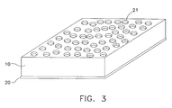
- Figure 3 shows a third embodiment of the invention in which the chiral elements are Möbius bands 21 which are superposed on the lossy dielectric material 10.
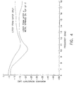
- Figures 4 and 5 show test results obtained with an absorbing structure according to the invention.
- the lossy dielectric used was one of the ECCOSORB LS (T.M.) range discussed above with an insertion loss of 7.5 dB at 3 gigahertz.
- the chiral elements used were metallic springs of the following typical dimensions: overall length 4.7mm; wire diameter .32mm; coil diameter 2.5mm; pitch 0.78mm. Such springs are available from TEVEMA under the specification D 10700.
- the tests were carried out on a 25cm square test piece with a surface density of springs corresponding to 4cm3 of the metal distributed homogeneously over the test piece. As can be seen, the insertion loss of the overall structure is markedly increased as compared with the lossy foam layer alone, an increase in insertion loss of up to 12 dB being achieved.
- Figure 6 shows a similar test carried out with a lossy dielectric foam of insertion loss 6.2 dB at 3 gigahertz and metallic springs of the D 10610 specification (TEVEMA). With approximately 1000 chiral elements on the 25cm square test piece an increase in reflection attenuation of between 10 and 14 dB can be noted.
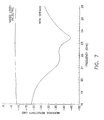
- Figure 7 shows the results of a test similar to that carried out above but with a lossy dielectric of approximately 5.7 dB insertion loss at 3 gigahertz and with 1450 springs of the D 10700 specification spread on the 25cm2 test piece. As can be seen, the reflection attenuation can be improved by up to 35 dB by the addition of the chiral elements.
- Figure 8 shows the results of a similar test with a lossy dielectric of insertion loss 7.3 dB at 3 gigahertz and chiral elements of the D 10610 specification (TEVEMA). The results are shown for instances where the helices are homogeneously distributed (the middle of the three curves) and where the helices are concentrated towards the centre of the test sample (the lower of the three curves). As can be seen, an improvement in reflection attenuation of up to 15 dB is possible.
- TEVEMA lossy dielectric of insertion loss 7.3 dB at 3 gigahertz and chiral elements of the D 10610 specification
- a concentration of helices on the lossy dielectric which corresponds to 6x10 ⁇ 3 - 10x10 ⁇ 3 cm3 of metal per cm2 of absorber surface is preferable but not essential.
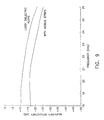
- Figure 9 shows the results of tests carried out on absorbers according to the invention in which the chiral elements are Möbius bands.
- the lossy dielectric medium was in this instance a lossy foam of 6.25 dB insertion loss at 3 GHz and the Möbius bands were formed of a carbon loaded polycarbonate ("Macrofol" available from Bayer).
- the Möbius bands are of 20cm length and 5mm wide. With a concentration of 36 rings on the 25cm square test piece, an increase in insertion loss of approximately 7 dB can be achieved.
- the lossy dielectric layer may also be shaped into forms which may be cones, wedges, pyramids or oblate spheroids as appropriate, and be made of materials with increasing insertion loss through their depth.
- Such shaped forms are well-known in the art and commercially available, e.g. ECCOSORB (T.M.) WG-NRL and ECCOSORB (T.M.) VHP-NRL pyramidal absorber available from Grace NV.
- Figure 10 shows a fourth embodiment of the invention in which the lossy dielectric medium 30 is shaped to form, in this instance a hollow wedge shown in cross section, for use in an anti-reflection structure, e.g. an anechoic chamber, a wall 33 of which is shown.
- the structure shown is hollow, although it may be solid and comprises chiral elements on its surface. These elements may either be "naked" or embedded in a non-lossy layer such as a foam 13.
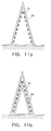
- Figures 11a and 11b show alternative embodiments to Figure 10 in which the chiral elements may be on the inside of the lossy dielectric structure, or may be enclosed between two substructures shaped to form the overall structure. In either instance the chiral elements may be embedded in a foam. Alternatively, the chiral elements may be arranged on one or more of the surfaces of the lossy dielectric shown in Figure 11b.
- coil springs or Möbius strips for the chiral elements include a) irregular tetrahedra, b) tapering coil springs (either with constant pitch and reducing diameter, or constant diameter or reducing pitch or a combination of both), c) screws or d) forks with at least three prongs which form an asymmetrical non planar structure. Improvements can also be obtained with mixtures of chiral elements of the same handedness but which give rise to different ⁇ values through the absorbing structure.
- Such chiral elements e.g. springs, need not be metallic but it is expected that they will be at least to some extent conductive, and may be of copper, carbonyl iron, brass, steel, a ferromagnetic metal or alloy, ceramic, graphite, or conductive polymer (whether inherently conductive, or conductive by addition).
Landscapes
- Engineering & Computer Science (AREA)
- Textile Engineering (AREA)
- Physics & Mathematics (AREA)
- Electromagnetism (AREA)
- Microelectronics & Electronic Packaging (AREA)
- Shielding Devices Or Components To Electric Or Magnetic Fields (AREA)
- Aerials With Secondary Devices (AREA)
- Diaphragms For Electromechanical Transducers (AREA)
- Materials For Medical Uses (AREA)
- Laminated Bodies (AREA)
Applications Claiming Priority (2)
| Application Number | Priority Date | Filing Date | Title |
|---|---|---|---|
| GB9114060 | 1991-06-28 | ||
| GB9114060A GB2257303A (en) | 1991-06-28 | 1991-06-28 | Chiral absorbing structure |
Publications (2)
| Publication Number | Publication Date |
|---|---|
| EP0520677A1 true EP0520677A1 (de) | 1992-12-30 |
| EP0520677B1 EP0520677B1 (de) | 1996-03-13 |
Family
ID=10697536
Family Applications (1)
| Application Number | Title | Priority Date | Filing Date |
|---|---|---|---|
| EP92305547A Expired - Lifetime EP0520677B1 (de) | 1991-06-28 | 1992-06-17 | Chiral absorbierende Struktur |
Country Status (6)
| Country | Link |
|---|---|
| US (1) | US5229773A (de) |
| EP (1) | EP0520677B1 (de) |
| AT (1) | ATE135522T1 (de) |
| DE (1) | DE69208952T2 (de) |
| GB (1) | GB2257303A (de) |
| ZA (1) | ZA923397B (de) |
Cited By (3)
| Publication number | Priority date | Publication date | Assignee | Title |
|---|---|---|---|---|
| EP0758803A1 (de) * | 1995-08-16 | 1997-02-19 | British Aerospace Public Limited Company | Herstellung von chiralem Verbundmaterial |
| WO2003054592A3 (en) * | 2001-12-20 | 2003-10-30 | Univ Southampton | Optical device |
| EP2439813A1 (de) * | 2010-10-07 | 2012-04-11 | Rheinmetall Waffe Munition GmbH | Täuschkörper zum Schutz von Objekten |
Families Citing this family (10)
| Publication number | Priority date | Publication date | Assignee | Title |
|---|---|---|---|---|
| US6252541B1 (en) | 1994-07-11 | 2001-06-26 | Mcdonnell Douglas Corporation | Low RCS test mounts |
| US5596324A (en) * | 1994-07-11 | 1997-01-21 | Mcdonnell Douglas Corporation | Electronic baffle and baffle controlled microwave devices |
| US5721553A (en) * | 1994-07-11 | 1998-02-24 | Mcdonnell Douglas Corporation | Low RCS test mounts |
| US5594218A (en) * | 1995-01-04 | 1997-01-14 | Northrop Grumman Corporation | Anechoic chamber absorber and method |
| JP2009094502A (ja) * | 2007-09-20 | 2009-04-30 | Nitto Denko Corp | 電磁波吸収体及び電磁波吸収方法 |
| US8687260B2 (en) * | 2007-12-28 | 2014-04-01 | Texas Instruments Incorporated | Solid-state optical modulator |
| WO2013144410A1 (es) * | 2012-03-30 | 2013-10-03 | Micromag 2000, S.L. | Atenuador de radiación electromagnética |
| EP3890115A1 (de) | 2013-03-15 | 2021-10-06 | Flextronics AP LLC | Verfahren und vorrichtung zur erzeugung perfekter mikrowellenabsorbierender leiterplatten |
| KR20240027058A (ko) | 2021-06-30 | 2024-02-29 | 쓰리엠 이노베이티브 프로퍼티즈 캄파니 | 전자기 제어 물품 |
| US11882680B2 (en) * | 2021-09-23 | 2024-01-23 | Vorbeck Materials Corp. | Electromagnetic interference shielding structures |
Citations (1)
| Publication number | Priority date | Publication date | Assignee | Title |
|---|---|---|---|---|
| WO1990003102A1 (en) * | 1988-09-15 | 1990-03-22 | The Pennsylvania State University | Electromagnetic shielding and absorptive materials |
Family Cites Families (4)
| Publication number | Priority date | Publication date | Assignee | Title |
|---|---|---|---|---|
| US2841736A (en) * | 1953-06-05 | 1958-07-01 | Rca Corp | Electron tube and filamentary cathode |
| WO1990004210A1 (en) * | 1988-10-07 | 1990-04-19 | The Trustees Of The University Of Pennsylvania | Electromagnetically non-reflective materials |
| US5063391A (en) * | 1989-06-06 | 1991-11-05 | The Trustees Of The University Of Penn. | Method of measuring chiral parameters of a chiral material |
| US5099242A (en) * | 1990-01-04 | 1992-03-24 | The Trustees Of The University Of Pennsylvania | Novel shielding, reflection and scattering control using chiral materials |
-
1991
- 1991-06-28 GB GB9114060A patent/GB2257303A/en not_active Withdrawn
-
1992
- 1992-04-10 US US07/866,593 patent/US5229773A/en not_active Expired - Lifetime
- 1992-05-11 ZA ZA923397A patent/ZA923397B/xx unknown
- 1992-06-17 DE DE69208952T patent/DE69208952T2/de not_active Expired - Fee Related
- 1992-06-17 EP EP92305547A patent/EP0520677B1/de not_active Expired - Lifetime
- 1992-06-17 AT AT92305547T patent/ATE135522T1/de not_active IP Right Cessation
Patent Citations (1)
| Publication number | Priority date | Publication date | Assignee | Title |
|---|---|---|---|---|
| WO1990003102A1 (en) * | 1988-09-15 | 1990-03-22 | The Pennsylvania State University | Electromagnetic shielding and absorptive materials |
Non-Patent Citations (1)
| Title |
|---|
| JOURNAL OF WAVE MATERIAL INTERACTION vol. 2, no. 1, January 1987, PHILADELPHIA, PENNSYLVANIA, US pages 71 - 81 V.K. VARADAN ET AL. 'On the possibility of designing anti-reflection coatings using chiral composites' * |
Cited By (3)
| Publication number | Priority date | Publication date | Assignee | Title |
|---|---|---|---|---|
| EP0758803A1 (de) * | 1995-08-16 | 1997-02-19 | British Aerospace Public Limited Company | Herstellung von chiralem Verbundmaterial |
| WO2003054592A3 (en) * | 2001-12-20 | 2003-10-30 | Univ Southampton | Optical device |
| EP2439813A1 (de) * | 2010-10-07 | 2012-04-11 | Rheinmetall Waffe Munition GmbH | Täuschkörper zum Schutz von Objekten |
Also Published As
| Publication number | Publication date |
|---|---|
| DE69208952T2 (de) | 1996-09-19 |
| US5229773A (en) | 1993-07-20 |
| EP0520677B1 (de) | 1996-03-13 |
| ZA923397B (en) | 1993-01-27 |
| DE69208952D1 (de) | 1996-04-18 |
| ATE135522T1 (de) | 1996-03-15 |
| GB9114060D0 (en) | 1991-08-21 |
| GB2257303A (en) | 1993-01-06 |
Similar Documents
| Publication | Publication Date | Title |
|---|---|---|
| EP0520677B1 (de) | Chiral absorbierende Struktur | |
| US4725490A (en) | High magnetic permeability composites containing fibers with ferrite fill | |
| US4539433A (en) | Electromagnetic shield | |
| KR100503133B1 (ko) | 복합자성체및전자간섭억제체 | |
| US4948922A (en) | Electromagnetic shielding and absorptive materials | |
| EP0764954A1 (de) | Magnetisches Kompositartikel zur Unterdrückung von elektromagnetischen Interferenzen | |
| US6137389A (en) | Inductor element for noise suppression | |
| DE112017002142B4 (de) | Millimeterwellenband-kommunikationsgerät | |
| CN109862769A (zh) | 一种超薄超宽谱的吸波材料及其制备方法 | |
| EP0689262B1 (de) | Wellenabsorbierende Zusammensetzung, Absorberelement für Funkwellen, Funkwellenabsorber und Verfahren zur Herstellung von Absorberelementen | |
| US4728554A (en) | Fiber structure and method for obtaining tuned response to high frequency electromagnetic radiation | |
| US6452564B1 (en) | RF surface wave attenuating dielectric coatings composed of conducting, high aspect ratio biologically-derived particles in a polymer matrix | |
| DE68909670T2 (de) | Elektrische Vorrichtung. | |
| US5202535A (en) | Chiral absorber | |
| KR0158081B1 (ko) | 복합형 광대역 전자파 흡수체 | |
| US20030198800A1 (en) | Plastic element for the confinement of HF reflections | |
| EP0439337A2 (de) | Breitbandiger Wellenabsorber | |
| EP0479438B1 (de) | Elektromagnetische Strahlung absorbierendes Material mit doppelt umhüllten Partikeln | |
| JP2001164124A (ja) | 樹脂複合体及びこれを用いた電波吸収体並びにその製造方法 | |
| JP5441211B2 (ja) | 複合型電波吸収体とそれを用いた電波吸収壁、電波暗室 | |
| Naito | Ferrite electromagnetic wave absorbers | |
| Truong et al. | Conducting-polymer-based radar-absorbing materials | |
| US20070277705A1 (en) | Carbonized shaped polymeric foam emi shielding enclosures | |
| McKinzie | On the surface wave properties of sievenpiper-type metamaterial absorbers | |
| JP2911264B2 (ja) | 広帯域フェライト電波吸収体 |
Legal Events
| Date | Code | Title | Description |
|---|---|---|---|
| PUAI | Public reference made under article 153(3) epc to a published international application that has entered the european phase |
Free format text: ORIGINAL CODE: 0009012 |
|
| AK | Designated contracting states |
Kind code of ref document: A1 Designated state(s): AT BE CH DE DK ES FR GB GR IT LI NL PT SE |
|
| 17P | Request for examination filed |
Effective date: 19930621 |
|
| 17Q | First examination report despatched |
Effective date: 19940121 |
|
| GRAA | (expected) grant |
Free format text: ORIGINAL CODE: 0009210 |
|
| AK | Designated contracting states |
Kind code of ref document: B1 Designated state(s): AT BE CH DE DK ES FR GB GR IT LI NL PT SE |
|
| PG25 | Lapsed in a contracting state [announced via postgrant information from national office to epo] |
Ref country code: NL Free format text: LAPSE BECAUSE OF FAILURE TO SUBMIT A TRANSLATION OF THE DESCRIPTION OR TO PAY THE FEE WITHIN THE PRESCRIBED TIME-LIMIT Effective date: 19960313 Ref country code: LI Effective date: 19960313 Ref country code: IT Free format text: LAPSE BECAUSE OF FAILURE TO SUBMIT A TRANSLATION OF THE DESCRIPTION OR TO PAY THE FEE WITHIN THE PRE;WARNING: LAPSES OF ITALIAN PATENTS WITH EFFECTIVE DATE BEFORE 2007 MAY HAVE OCCURRED AT ANY TIME BEFORE 2007. THE CORRECT EFFECTIVE DATE MAY BE DIFFERENT FROM THE ONE RECORDED.SCRIBED TIME-LIMIT Effective date: 19960313 Ref country code: GR Free format text: LAPSE BECAUSE OF FAILURE TO SUBMIT A TRANSLATION OF THE DESCRIPTION OR TO PAY THE FEE WITHIN THE PRESCRIBED TIME-LIMIT Effective date: 19960313 Ref country code: ES Free format text: THE PATENT HAS BEEN ANNULLED BY A DECISION OF A NATIONAL AUTHORITY Effective date: 19960313 Ref country code: DK Effective date: 19960313 Ref country code: CH Effective date: 19960313 Ref country code: BE Effective date: 19960313 Ref country code: AT Effective date: 19960313 |
|
| REF | Corresponds to: |
Ref document number: 135522 Country of ref document: AT Date of ref document: 19960315 Kind code of ref document: T |
|
| REF | Corresponds to: |
Ref document number: 69208952 Country of ref document: DE Date of ref document: 19960418 |
|
| PG25 | Lapsed in a contracting state [announced via postgrant information from national office to epo] |
Ref country code: SE Effective date: 19960613 |
|
| PG25 | Lapsed in a contracting state [announced via postgrant information from national office to epo] |
Ref country code: PT Effective date: 19960614 |
|
| ET | Fr: translation filed | ||
| NLV1 | Nl: lapsed or annulled due to failure to fulfill the requirements of art. 29p and 29m of the patents act | ||
| PLBE | No opposition filed within time limit |
Free format text: ORIGINAL CODE: 0009261 |
|
| STAA | Information on the status of an ep patent application or granted ep patent |
Free format text: STATUS: NO OPPOSITION FILED WITHIN TIME LIMIT |
|
| 26N | No opposition filed | ||
| REG | Reference to a national code |
Ref country code: FR Ref legal event code: TP |
|
| REG | Reference to a national code |
Ref country code: GB Ref legal event code: IF02 |
|
| PGFP | Annual fee paid to national office [announced via postgrant information from national office to epo] |
Ref country code: FR Payment date: 20020426 Year of fee payment: 11 |
|
| PGFP | Annual fee paid to national office [announced via postgrant information from national office to epo] |
Ref country code: GB Payment date: 20020612 Year of fee payment: 11 |
|
| PGFP | Annual fee paid to national office [announced via postgrant information from national office to epo] |
Ref country code: DE Payment date: 20020626 Year of fee payment: 11 |
|
| PG25 | Lapsed in a contracting state [announced via postgrant information from national office to epo] |
Ref country code: GB Free format text: LAPSE BECAUSE OF NON-PAYMENT OF DUE FEES Effective date: 20030617 |
|
| PG25 | Lapsed in a contracting state [announced via postgrant information from national office to epo] |
Ref country code: DE Free format text: LAPSE BECAUSE OF NON-PAYMENT OF DUE FEES Effective date: 20040101 |
|
| GBPC | Gb: european patent ceased through non-payment of renewal fee |
Effective date: 20030617 |
|
| PG25 | Lapsed in a contracting state [announced via postgrant information from national office to epo] |
Ref country code: FR Free format text: LAPSE BECAUSE OF NON-PAYMENT OF DUE FEES Effective date: 20040227 |
|
| REG | Reference to a national code |
Ref country code: FR Ref legal event code: ST |
|
| REG | Reference to a national code |
Ref country code: CH Ref legal event code: PL Ref country code: CH Ref legal event code: EP |