EP0520837A2 - Wirksamer Arbiter - Google Patents
Wirksamer Arbiter Download PDFInfo
- Publication number
- EP0520837A2 EP0520837A2 EP19920305983 EP92305983A EP0520837A2 EP 0520837 A2 EP0520837 A2 EP 0520837A2 EP 19920305983 EP19920305983 EP 19920305983 EP 92305983 A EP92305983 A EP 92305983A EP 0520837 A2 EP0520837 A2 EP 0520837A2
- Authority
- EP
- European Patent Office
- Prior art keywords
- output
- input
- flip
- signals
- arbiter
- Prior art date
- Legal status (The legal status is an assumption and is not a legal conclusion. Google has not performed a legal analysis and makes no representation as to the accuracy of the status listed.)
- Granted
Links
Images


Classifications
-
- G—PHYSICS
- G06—COMPUTING OR CALCULATING; COUNTING
- G06F—ELECTRIC DIGITAL DATA PROCESSING
- G06F13/00—Interconnection of, or transfer of information or other signals between, memories, input/output devices or central processing units
- G06F13/14—Handling requests for interconnection or transfer
- G06F13/36—Handling requests for interconnection or transfer for access to common bus or bus system
- G06F13/362—Handling requests for interconnection or transfer for access to common bus or bus system with centralised access control
- G06F13/364—Handling requests for interconnection or transfer for access to common bus or bus system with centralised access control using independent requests or grants, e.g. using separated request and grant lines
-
- H—ELECTRICITY
- H03—ELECTRONIC CIRCUITRY
- H03K—PULSE TECHNIQUE
- H03K5/00—Manipulating of pulses not covered by one of the other main groups of this subclass
- H03K5/22—Circuits having more than one input and one output for comparing pulses or pulse trains with each other according to input signal characteristics, e.g. slope, integral
Definitions
- the present invention is directed to resource allocation and arbitration in a computer system and, more particularly, to an implementation efficient logic circuit used as an arbiter to control access to a shared resource by N devices.
- Modern computer systems often comprise a plurality of operating devices such as processors and I/O controllers and a shared resource such as a shared memory.
- the shared memory is made available to each of the plurality of devices in the computer system as a memory service for the storage of data.
- the processors, I/O controllers and the shared resource are coupled to one another by a bus and only one device at a time can access the shared resource over the bus. Accordingly, it is necessary to provide an arbitration scheme in the computer system to decide which one of several devices that may be requesting access to the shared memory will be granted control of the bus for the performance of read and write operations with the shared memory.
- a known method for implementing an arbitration scheme in a computer system consists of reducing a flow chart description of the logic required for the arbitration scheme into a gate level logic circuit implementation through the use of Karnaugh maps which are displays of truth tables wherein simplification of a Boolean expression is facilitated.
- the gate level implementation comprises a state machine wherein input signals corresponding to requests by the devices for access to the shared resource result in the generation of state variables that indicate which device has won the arbitration.
- a problem with the presently utilized gate level implementations for arbitration schemes is that the design uses only state variables and input signals to generate the next state variables.
- unused or invalid states for the state variables of the state machine are typically placed in the logic design so as to transition to a null state or to zero.
- presently known arbitration scheme implementations often require the use of a large number of components and gates to generate the necessary state variables, resulting in excessive cost and complexity.
- the present invention provides an implementation efficient logic circuit that functions as an arbiter to arbitrate amongst N devices of a computer system for access to a shared resource.
- the arbiter according to the present invention implements a logic design wherein next state variables utilized to indicate which device has won the arbitration are generated through the use of input signals, state variables and internally generated intermediate arbitration win signals coupled to one another in the logic design.
- the invention in its broad form resides in a logic circuit for generating a set of output signals in response to and as a function of a set of input signals, the circuit comprising: a set of N logic gates, each having N inputs, with one of the N inputs being used for application of one of the set of input signals, and an output; a set of N state elements, each one of the state elements having an input coupled to the output of a corresponding one of the N logic gates, and an output to provide one of the set of output signals; for each nth logic gate of the N logic gates, each of (N-n) remaining inputs, when n ⁇ N, is coupled to the output of a corresponding one of the n+1th to Nth state elements of the N state elements and each of n-1 remaining inputs, when n>1, is coupled to the output of a corresponding one of the 1st to (n-1)th logic gates; such that the set of output signals is a function of the set of input signals and the output of the set of N logic gates.
- each unused or invalid state in the logic design is selected so that each invalid state transitions to a valid state.
- the use of intermediate arbitration win signals and present state variables in, e.g., a NOR gate array, and the positioning of invalid states that result in a transition to a valid state provides a minimal solution for the logic design with a significant reduction in the total number of components that would be required to implement an arbitration logic using conventional design techniques.
- the resulting arbiter will have the advantage of being more cost effective than conventional arbiter designs and provides a smaller physical solution for a required arbitration scheme.
- Figure 1 illustrates a computer system comprising a plurality of devices coupled to each of a common resource and an arbiter according to a preferred embodiment of the present invention.
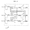
- Figure 2 illustrates a schematic diagram of the arbiter of Fig. 1.
- Figure 3 illustrates a state diagram for the arbiter of Fig. 2.
- Figure 4 illustrates a present state/next state table for the arbiter of Fig. 2.
- Figure 5 illustrates a schematic diagram of an N input arbiter according to the present invention.
- FIG. 1 there is illustrated a computer system 10 comprising three devices 12, 14, 16 and a shared resource 18.
- Each of the devices 12, 14, 16 can be a processor and the shared resource 18 can comprise a shared memory.
- the processors 12, 14, 16 and the shared memory 18 are coupled to one another by a bus 20.
- each of the processors 12, 14, 16 can control the bus 20 at any one time for access to the shared memory 18. Accordingly, each of the processors 12, 14, 16 is coupled to an arbiter 22 by a request line R1(L), R2(L) and R3(L), respectively. When any one of the processors 12, 14, 16 requires access to the shared memory 18, it will assert a request signal, low active, on its respective request line R1(L), R2(L), R3(L) .
- the arbiter 22 comprises a state machine arranged to generate state variables W1(H), W2(H), W3(H) as a function of the assertion of requests R1(L), R2(L), R3(L) by the processors 12, 14, 16.
- the state variables W1(H), W2(H), W3(H) are coupled to the processors 12, 14, 16, respectively, with either none of the state variables W1(H), W2(H), W3(H) being asserted or a single state variable W1(H), W2(H), or W3(H) being asserted, high active, at any one time to indicate which one of the processors 12, 14, 16 has been granted access to the shared memory 18.
- the state variables W1(H), W2(H), W3(H) output by the arbiter 22 are supplied as respective inputs to the devices 12, 14, 16 with each state variable W1(H), W2(H), W3(H) indicating to a particular device 12, 14, 16 whether it has been granted access to the shared memory 18.
- the arbiter 22 of Figure 1 is illustrated in greater detail in Figure 2.
- the requests, R1(L), R2(L)and R3(L) are input to the arbiter 22 as asynchronous signals.
- Each request indicates whether the respective device 12, 14, 16 wants access to the shared memory 18.
- the requests are each asserted low active when the respective processor 12, 14, 16 wants access to the shared memory 18 and each request R1(L), R2(L), R3(L) is input to a respective one of a first stage of three flip-flops 24, 26, 28.
- the flip-flops 24, 26, 28 are used to synchronize the asynchronous requests R1(L), R2(L), R3(L) and output corresponding synchronized access request signals RS1(L), RS2(L), RS3(L).
- a second stage of three D-type flip-flops 30, 32, 34 represents the three state variables W1(H), W2(H), W3(H).
- the combinational logic of the arbiter 22 illustrated in Fig. 2 includes a series of three NOR-gates 36, 38, 40 arranged to couple the first stage of flip-flops 24, 26, 28 to the second stage of D-type flip-flops 30, 32, 34.
- the NOR-gates 36, 38, 40 operate to arbitrate the three synchronized requests RS1(L), RS2(L), RS3(L) and thereby generate three intermediate arbitration win output signals RW1(H), RW2(H), RW3(H) that are used as inputs to the D-type flip-flops 30, 32, 34, respectively. Accordingly, on the next clock edge, only one of the state variables W1(H), W2(H) or W3(H) is asserted, as will appear.
- the arbiter 22 of the present invention couples each of the state variables W2(H) and W3(H), output from the second and third ones of the second-stage flip-flops 32, 34, as input signals to each preceding one of the first and second NOR gates 36, 38, respectively, and couples each of the outputs of the first and second ones of the Nor gates 36, 38, RW1(H) and RW2(H), as input signals to the second and third NOR gates 36, 38, respectively.
- the arbiter 22 uses both the state variables W2(H), W3(H) and the previously generated intermediate arbitration win signals RW1(H) and RW2(H), in the generation of the inputs to the D-type flip-flops 30, 32, 34.
- the first asynchronous request R1(L), from the processor 12, is applied to the input of the first flip-flop 24 of the first stage of flip-flops.
- the output of the first flip-flop 24, RS1(L), is coupled to one of the inputs of the first NOR gate 36.
- the remaining inputs to the first NOR gate 36 are coupled to the outputs of the second and third ones of the second-stage flip-flops 32, 34, respectively.
- the synchronized access request signal RS1(L), output from the first flip-flop 24, is input into the first NOR gate 36 with the state variables W2(H) and W3(H) being used as second and third inputs to the first NOR gate 36.
- the output of the first NOR gate 36, RW1(H), is coupled to the input of the first one of the second-stage flip-flops 30 and to the inputs of each of the second and third NOR gates 38, 40.
- the state variable W1(H), output from the first one of the second-stage flip-flops 30, is coupled to the first processor 12 (See Fig. 1).
- the second asynchronous request R2(L), from the processor 14, is applied to the input of the second flip-flop 26 of the first stage of flip-flops.
- the second synchronous access request RS2(L) is output from the second flip-flop 26 and is applied as an input to one of the inputs of the second NOR gate 38.
- Another input to the second NOR gate 38 is coupled to the output RW1(H) of the first NOR gate 32 while the remaining input to the second NOR gate 38 is coupled to the output W3(H), of the third one of the second stage flip-flops 34.
- the second or gate 38 receives the signals RS2(L), RW1(H) and W3(H) as its three inputs, respectively.
- the output of the second NOR gate 38 is coupled to the input of the second one of the second stage flip-flops 32 and to an input of the third NOR gate 40.
- both the second-stage flip-flop 32 and the third NOR gate 40 receive the output, RW2(H), of the second NOR gate 38, as an input.
- the output of the second-stage flip-flop 32 is coupled to the input of the first NOR gate 36 and to the second processor 14.
- the first NOR gate 36 has the output of the second-stage flip-flop 10, the state variable W2(H), as one of its inputs.
- the asynchronous request R3(L), from the processor 16, is input into the third flip-flop 28.
- the third synchronous access request RS3(L) output by the third flip-flop 38 serves as an input to the third NOR gate 40.
- the third NOR gate 40 includes two other inputs coupled to the outputs of the first and second NOR gates 36, 38, respectively.
- the output of the first Nor gate 36, RW1(H), and the output of the second NOR gate 38, RW2(H) each serve as inputs to the third Nor gate 40.
- the output of the third NOR gate 40 is the signal RW3(H) which serves as an input to the third of the second-stage flip-flops 34.
- the output of the third second-stage flip-flop 34 is coupled to the third processor 16 and to an input of each of the first and second Nor gates 36, 38.
- the output of the third second-stage flip-flop 34, the state variable W3(H) is provided as an input to each of the first and second NOR gates 36, 38.
- Figure 3 shows a state diagram flow chart for implementing the three input arbiter 22 of Figure 2, with all unused states accounted for.
- a block 15 represents state A in which the state variables W3(H), W2(H), W1(H) have the present values 0,0,0 respectively.
- the synchronized access request signal RS1(L) is low, and the arbiter 22 transitions to a state B, represented by block 19, in which the state variables W3(H), W2(H), W1(H) have the values 0,0,1 respectively.
- the arbiter 22 remains in state B 19 as long as the first processor 12 continues to assert a request RS1(L) for access to the shared memory 18.
- the arbiter 22 transitions into a state C, represented by block 21, a state D, represented by block 23 or back to state A 15.
- the state the arbiter 22 transitions to depends on whether the second or third processors 14, 16 have or have not asserted a request signal R2(L) or R3(L).
- state variables W3(H), W2(H), W1(H) have the values 0,1,0 while in state D 18 they have the values 1,0,0, respectively.
- the arbiter 22 transitions into state A 15 and remains there until a request RS1(L), RS2(L) or RS3(L) is asserted.
- the arbiter 22 transitions into state C 17 (block 17 represents no and block 25 represents yes). Once in state C 17, the arbiter 22 remains in that state so long as the second processor 14 continues to assert the access request signal R2(L) for access to the shared memory 18. when the second processor 14 no longer asserts the access request R2(L), the arbiter 22 transitions into state D 23 if the third processor 16 has asserted an access request RS3(L) (block 27 yes). Otherwise, the arbiter 22 transitions back to state A 15 (block 27 no).
- the arbiter 22 When none of the processors 12, 14, 16 are asserting a request for access to the shared memory 18, the arbiter 22 remains in state A 15 until a request RS1(L), RS2(L) or RS3(L) is asserted (blocks 17, 25, 27).
- state variables indicate one of the requesting devices that has been granted access to the shared resource.
- the four invalid states include each possible state wherein more than one of the state variables are asserted and are defined by the state variables W3(H), W2(H), W1(H) having the values (state E: 0,1,1); (state F: 1,1,0); (state G: 1,1,1); or (state H: 1,0,1).
- state E will transition to block 25 and states F, G, and H will transition to block 27.
- Figure 4 illustrates a present state/next state table derived from the state diagram of Figure 3, for the arbiter 22 of Figure 2.
- the state table contains a first column 50 listing the present state values of the state variables W3(H), W2(H), and W1(H) respectively.
- a second column 51 lists the values of the three synchronized input signals RS3(L), RS2(L), and RS1(L).
- a third column 52 of the state table lists the next state values for the state variables W3(H), W2(H), and W1(H) given the present state values of the first column 50 and the input values of the second column 51.
- the presence of an x in the second column 51 represents a "don't care" condition. This means that the value of the input RS3(L), RS2(L) or RS1(L), represented by an x in column 51, can assume either the value of a 1 or a 0 (high or low) without affecting the operation of the arbiter 22 or the next state that the arbiter 22 will enter.
- the arbiter 22 of Fig. 2 utilizes the set of three input NOR gates 36, 38, 40 to generate intermediate arbitration win signals RW1(H), RW2(H) and RW3(H).
- the signals RW1(H), RW2(H), RW3(H) provide both a series of input signals for the corresponding flip-flops 30, 32, 34 of the second set of flip-flops to generate the state variables W1(H), W2(H), W3(H) and a series of inputs to relatively subsequent NOR gates 38, 40 of the set of NOR gates.
- state variables W1(H), W2(H) and W3(H) provide indications of an arbitration win to the respective processors 12, 14, 16 and a series of inputs to relatively preceding NOR gate 36, 38 of the set of NOR gates.
- the design of the arbiter 22 permits the arbitration scheme to be implemented with three input NOR gates and only two stages of logic subsequent to the request signal synchronization stage.
- D-type flip-flops 30, 32, 34 are utilized for the second stage of flip-flops.
- the use of D-type flip-flops makes it necessary to define when the input of each flip-flop is in a high state, i.e., a "1".
- the input to state variable W1(H) is RW1(H)
- the input to state variable W2(H) is RW2(H)
- the input to state variable W3(H) is RW3(H).
- a "-" in front of a signal name indicates a "NOT" function.
- RW1(H) -( W3(H) + W2(H) + RS1(L) ) and may be implemented through the use of a three input NOR gate.
- RW2(H) -W3(H).-RS2(L).( RS1(L) + W2(H) )
- This solution requires logic for four terms (W3(H), RS2(L), RS1(L) and W2(H) ), when expressed solely in terms of inputs and state variables and is not suitable for a three input NOR gate.
- RW1(H), RW2(H) and RW3(H) are the standard minimum sum of the products form expressed in terms of inputs and state variables and used in conventional logic circuits. As can be seen, neither of the conventional minimum sum solutions for RW2(H) and RW3(H) can be implemented in a three input NOR gate.
- the new efficient implementation design illustrated in Fig. 2 is based upon the known minimum sum of the products form set forth above.
- RW2(H) -W3(H) .-RS2(L) .
- W3(H) + RS1(L) + W2(H) substituting RW1(H) for (W3(H) + RS1(L) + W2(H)
- RW2(H) -W3(H).-RS2(L).-RW1(H) applying De Morgan's Logic theorems:
- RW2(H) -( W3(H) + RS2(L) + RW1(H) )
- RW3(H) -( RS3(L) + RW1(H) + RW2(H) ) which may be implemented through the use of a three input NOR gate.
- FIG. 5 illustrates an N input arbiter implemented in accordance with the design principles of the present invention.
- Asynchronous access requests R1(L), R2(L), ..., R(N) (L) are applied to the inputs of the N first stage flip-flops 126, 127, 128, 129, referred to as FS1(1), FS1(2), ..., FS1(N-1), FS1(N) respectively.
- the term FS1(n) is used to refer to the n th flip-flop in the 1 st stage of the arbiter.
- the term FS2(n) will be used to refer to the n th flip-flop in the second stage of flip-flop of the arbiter.
- the NOR gates 130, 131, 132, 133 shall be referred to in a similar manner as NR1 130 through NR(N) 133.
- the synchronized requests RS1(L), RS2(L), ... RSN(L) for access to the shared resource are the outputs of the respective first stage flip-flops FS11, FS12, ..., FS1N 126-129.
- the input to the first stage flip-flop FS11 126 is the asynchronous access request signal R1(L) output from a first device requesting access to a shared resource.
- the output of the first stage flip-flop FS11 126, RS1(L) is coupled to an input of an N input NOR gate 130 referred to as NR1.
- the remaining N-1 inputs of the NOR gate NR1 130 are coupled to the outputs of the second stage flip-flops 135, 136, 137 referred to as FS2(2) through FS2(N). In this manner, the state variables W2(H) through WN(H) are applied as inputs to NOR gate NR1 130.
- the output of NOR gate NR1 130 is coupled to the input of the second stage flip-flop FS21 134 and to an input of each of the NOR gates NR2 131 through NRN 133. Therefore, the output signal RW1(H) of NOR gate NR1 130 is applied to the input of flip-flop FS2(1) 134 and is also applied as an input to NOR gates NR2 131 through NR(N) 133, respectively.
- the output of the flip-flop FS2(1) 134 is the state variable W1(H).
- the input to the first stage flip-flop FS1(2) 127 is the asynchronous access request signal R2(L) from a second device.
- the output terminal of flip-flop FS1(2) 127, RS2((L), is coupled to an input of the Nor gate NR2 131.
- Another input of the NOR gate NR2 131 is coupled to the output of the NOR gate NR1 130.
- the remaining N-2 inputs to the NOR gate NR2 131 are coupled to the respective outputs of the second stage flip-flops FS2(3) through FS2(N) 137.
- the output of the NOR gate NR2 131, RW2(H), is coupled to the input of FS2(2) 135 and an input of each of the respective NOR gates NR3 through NR(N) 33.
- FS22 35 and the respective NOR gates NR3 through NR(N) 33 all have the output signal of NR2 31, RW2(H), as an input signal.
- the output W2(H) of the second stage flip-flop FS2(2) 135 is coupled to an input of the NOR gate NR1 130.
- the asynchronous access request R(N-1) (L) serves as the input to the first stage (N-1) flip-flop FS1(N-1) 128.
- the output of FS1(N-1) 128, RS(N-1) (L) is coupled to an input of NOR gate NR(N-1) 132.
- the outputs of NOR gates NR1 30 through NR(N-2) are also coupled to respective inputs of NR(N-1) 132, applying the NOR gate output signals RW1(H) through RW(N-2) (H) as inputs to NR(N-1) 132.
- the remaining input of NR(N-1) 132 is coupled to the output of the flip-flop FS2(N) 137.
- the state variable WN(H) output by FS2(N) 137 is therefore an input to the NOR gate NR(N-1) 132.
- the output of the NOR gate NR(N-1) 132 is coupled to the input of the flip-flop FS2(N-1) 136 and to an input of the NOR gate NR(N) 132.
- the output signal RW(N-1) (H) from NR(N-1) 132 serves as an input signal to both FS2(N-1) 136 and NR(N) 133.
- the output of flip-flop FS2(N-1) 136 is coupled to an input of each of the NOR gates NR1 30 through NR(N-2) respectively.
- the sate variable W(N-1) (H) output by FS2(N-1) 136 is an input to NR1 30 through NR(N-2).
- the asynchronous access request signal RN(L) from the Nth device is input into the flip-flop FS1(N) 129.
- the output of FS1(N) 129, rsn(L) is coupled to an input of the NOR gate NR(N) 133.
- the remaining N-1 inputs to NR(N) are coupled to the outputs of NOR gates NR1 130 through NR(N-1) 132, respectively.
- the NOR gate output signals RW1(H) through RW(N-1) (H) are all inputs to the NOR gate NR(N) 133.
- NR(N) 133, RWN(H) The output of NR(N) 133, RWN(H), is coupled to the input of flip-flop FS2(N) 137.
- the output of FS2(N) 37 is coupled to inputs of the NOR gates NR1 30 through NR(N-1) 32.
- the state variable WN(H) is an input to NOR gates NR1 30 through NR(N-1) 32.
- the output of the flip-flop FS1(n) is coupled to an input of an N input NOR gate NR(n).
- RS(n) (L) the synchronized access request signal output from FS1(n) is an input to the NOR gate NR(n).
- Another (n-1) inputs to the NOR gate NR(n) are coupled to the outputs of the previous NOR gates NR1 through NR(n-1) when (n > 1). In this way, the output signals RW1(H) through RW(n-1) from the previous NOR gates, become inputs to NR(n) when (n > 1).
- the remaining (N-n) inputs to NR(n) are coupled to the outputs of the second stage flip-flops FS2(n+1) through FS2(N) when (n ⁇ N).
- the output of the NOR gate NR(n) is coupled to the input of the flip-flop FS2(n) and an input to each of the NOR gates NR(n+1) through NR(N) when (n ⁇ N).
- the signal RW(n) (H), output by NR(n) is therefore an input to FS2(n) and the NOR gates NR(n+1) through NR(N) when (n ⁇ N).
- the second stage flip-flop FS2(n) has its output coupled to inputs of the previous NOR gates NR1 through NR(n-1) when (n > 1).
- the state variable W(n) (H) which is the output of FS2(n) is an input signal to NOR gates NR1 through NR(n-1) when (n > 1).
Landscapes
- Physics & Mathematics (AREA)
- Engineering & Computer Science (AREA)
- Theoretical Computer Science (AREA)
- Nonlinear Science (AREA)
- General Engineering & Computer Science (AREA)
- General Physics & Mathematics (AREA)
- Bus Control (AREA)
Applications Claiming Priority (2)
| Application Number | Priority Date | Filing Date | Title |
|---|---|---|---|
| US723055 | 1991-06-28 | ||
| US07/723,055 US5148112A (en) | 1991-06-28 | 1991-06-28 | Efficient arbiter |
Publications (3)
| Publication Number | Publication Date |
|---|---|
| EP0520837A2 true EP0520837A2 (de) | 1992-12-30 |
| EP0520837A3 EP0520837A3 (en) | 1993-09-08 |
| EP0520837B1 EP0520837B1 (de) | 1998-04-15 |
Family
ID=24904642
Family Applications (1)
| Application Number | Title | Priority Date | Filing Date |
|---|---|---|---|
| EP92305983A Expired - Lifetime EP0520837B1 (de) | 1991-06-28 | 1992-06-29 | Wirksamer Arbiter |
Country Status (5)
| Country | Link |
|---|---|
| US (1) | US5148112A (de) |
| EP (1) | EP0520837B1 (de) |
| JP (1) | JPH05197673A (de) |
| DE (1) | DE69225095T2 (de) |
| IE (1) | IE922100A1 (de) |
Cited By (1)
| Publication number | Priority date | Publication date | Assignee | Title |
|---|---|---|---|---|
| EP0704807A1 (de) * | 1994-09-29 | 1996-04-03 | Xerox Corporation | Programmierbare Arbitrierungsvorrichtung |
Families Citing this family (12)
| Publication number | Priority date | Publication date | Assignee | Title |
|---|---|---|---|---|
| US5535395A (en) * | 1992-10-02 | 1996-07-09 | Compaq Computer Corporation | Prioritization of microprocessors in multiprocessor computer systems |
| US5553310A (en) * | 1992-10-02 | 1996-09-03 | Compaq Computer Corporation | Split transactions and pipelined arbitration of microprocessors in multiprocessing computer systems |
| US5553248A (en) * | 1992-10-02 | 1996-09-03 | Compaq Computer Corporation | System for awarding the highest priority to a microprocessor releasing a system bus after aborting a locked cycle upon detecting a locked retry signal |
| US5524235A (en) * | 1994-10-14 | 1996-06-04 | Compaq Computer Corporation | System for arbitrating access to memory with dynamic priority assignment |
| US5539337A (en) * | 1994-12-30 | 1996-07-23 | Intel Corporation | Clock noise filter for integrated circuits |
| US6163828A (en) * | 1998-05-22 | 2000-12-19 | Lucent Technologies Inc. | Methods and apparatus for providing multi-processor access to shared memory |
| EP1428330B1 (de) * | 2001-09-20 | 2005-05-25 | Honeywell, Inc. | Telefonsteuerung im einem flugdeck |
| WO2006082458A1 (en) * | 2005-01-31 | 2006-08-10 | Freescale Semiconductor, Inc. | Bus arbitration controller with reduced energy consumption |
| JP6354172B2 (ja) * | 2014-01-20 | 2018-07-11 | 富士通株式会社 | 半導体集積回路及び認証システム |
| DE102016215362A1 (de) * | 2016-08-17 | 2018-02-22 | Robert Bosch Gmbh | Quantenzufallszahlengenerator und Verfahren zum Erzeugen einer Zufallszahl mit einem Quantenzufallszahlengenerator |
| AU2020202306B2 (en) * | 2019-04-02 | 2025-05-15 | The Raymond Corporation | Systems and methods for an arbitration controller to arbitrate multiple automation requests on a material handling device |
| CN111752876B (zh) * | 2020-05-26 | 2023-03-14 | 苏州浪潮智能科技有限公司 | 一种用于接口优先级仲裁的系统 |
Family Cites Families (8)
| Publication number | Priority date | Publication date | Assignee | Title |
|---|---|---|---|---|
| US4237534A (en) * | 1978-11-13 | 1980-12-02 | Motorola, Inc. | Bus arbiter |
| US4620118A (en) * | 1982-10-01 | 1986-10-28 | At&T Bell Laboratories | Dual port access circuit with automatic asynchronous contention resolving capability |
| US4594657A (en) * | 1983-04-22 | 1986-06-10 | Motorola, Inc. | Semaphore for memory shared by two asynchronous microcomputers |
| US4641266A (en) * | 1983-11-28 | 1987-02-03 | At&T Bell Laboratories | Access-arbitration scheme |
| EP0257061A1 (de) * | 1986-02-10 | 1988-03-02 | EASTMAN KODAK COMPANY (a New Jersey corporation) | Vielfachprozessorvorrichtung |
| US4853653A (en) * | 1988-04-25 | 1989-08-01 | Rockwell International Corporation | Multiple input clock selector |
| US4894565A (en) * | 1988-08-11 | 1990-01-16 | American Microsystems, Inc. | Asynchronous digital arbiter |
| JP2569790B2 (ja) * | 1989-03-13 | 1997-01-08 | 三菱電機株式会社 | アービタ回路 |
-
1991
- 1991-06-28 US US07/723,055 patent/US5148112A/en not_active Expired - Lifetime
-
1992
- 1992-06-25 JP JP4167629A patent/JPH05197673A/ja active Pending
- 1992-06-29 DE DE69225095T patent/DE69225095T2/de not_active Expired - Fee Related
- 1992-06-29 EP EP92305983A patent/EP0520837B1/de not_active Expired - Lifetime
- 1992-07-01 IE IE210092A patent/IE922100A1/en not_active Application Discontinuation
Cited By (2)
| Publication number | Priority date | Publication date | Assignee | Title |
|---|---|---|---|---|
| EP0704807A1 (de) * | 1994-09-29 | 1996-04-03 | Xerox Corporation | Programmierbare Arbitrierungsvorrichtung |
| US5682467A (en) * | 1994-09-29 | 1997-10-28 | Xerox Corporation | Arbitrating apparatus for controlling selective access of multiple bus masters to a printing system video bus |
Also Published As
| Publication number | Publication date |
|---|---|
| EP0520837B1 (de) | 1998-04-15 |
| JPH05197673A (ja) | 1993-08-06 |
| DE69225095T2 (de) | 1998-12-17 |
| EP0520837A3 (en) | 1993-09-08 |
| IE922100A1 (en) | 1992-12-30 |
| US5148112A (en) | 1992-09-15 |
| DE69225095D1 (de) | 1998-05-20 |
Similar Documents
| Publication | Publication Date | Title |
|---|---|---|
| US5263172A (en) | Multiple speed synchronous bus having single clock path for providing first or second clock speed based upon speed indication signals | |
| US5455915A (en) | Computer system with bridge circuitry having input/output multiplexers and third direct unidirectional path for data transfer between buses operating at different rates | |
| US5175819A (en) | Cascadable parallel to serial converter using tap shift registers and data shift registers while receiving input data from FIFO buffer | |
| US4423384A (en) | Asynchronous multi-port arbiter | |
| US4503490A (en) | Distributed timing system | |
| US5574867A (en) | Fast first-come first served arbitration method | |
| US5654988A (en) | Apparatus for generating a pulse clock signal for a multiple-stage synchronizer | |
| EP0520837B1 (de) | Wirksamer Arbiter | |
| US4841178A (en) | Asynchronous processor arbitration circuit | |
| EP0122773A2 (de) | Arbitervorrichtung und Verfahren für die Verwendung in einem digitalen Datenverarbeitungssystem mit verschiedenen Bussteuerungseinrichtungen | |
| GB2202977A (en) | Computer system having direct memory access | |
| EP0242879B1 (de) | Datenprozessor mit Wartesteuerung, die Hochgeschwindigkeitszugriff gestattet | |
| EP0261497B1 (de) | Semaphorschaltung für gemeinsam genutzte Speicherzellen | |
| US5535343A (en) | Method and apparatus for generating write signals | |
| US5537582A (en) | Bus interface circuitry for synchronizing central processors running at multiple clock frequencies to other computer system circuitry | |
| US5875339A (en) | Asynchronous arbiter using multiple arbiter elements to enhance speed | |
| US5713025A (en) | Asynchronous arbiter using multiple arbiter elements to enhance speed | |
| US6853218B1 (en) | Multiport arbitration using phased locking arbiters | |
| US3377621A (en) | Electronic data processing system with time sharing of memory | |
| US5175832A (en) | Modular memory employing varying number of imput shift register stages | |
| KR0159008B1 (ko) | 직접 메모리 억세스에서의 버스사용 중재회로 | |
| EP0432463A2 (de) | Verteiltes, unparteiisches Arbitrierungsschema für Zugriff auf einen Datenübertragungsbus | |
| US4894769A (en) | Increased bandwith for multi-processor access of a common resource | |
| US5249154A (en) | Data access controller and method | |
| EP0087266B1 (de) | Prioritätsauflösungsschaltung |
Legal Events
| Date | Code | Title | Description |
|---|---|---|---|
| PUAI | Public reference made under article 153(3) epc to a published international application that has entered the european phase |
Free format text: ORIGINAL CODE: 0009012 |
|
| AK | Designated contracting states |
Kind code of ref document: A2 Designated state(s): DE FR GB IT |
|
| 17P | Request for examination filed |
Effective date: 19921102 |
|
| RIN1 | Information on inventor provided before grant (corrected) |
Inventor name: GAHAN, RICHARD A. |
|
| PUAL | Search report despatched |
Free format text: ORIGINAL CODE: 0009013 |
|
| RHK1 | Main classification (correction) |
Ipc: G06F 13/364 |
|
| AK | Designated contracting states |
Kind code of ref document: A3 Designated state(s): DE FR GB IT |
|
| 17Q | First examination report despatched |
Effective date: 19961008 |
|
| GRAG | Despatch of communication of intention to grant |
Free format text: ORIGINAL CODE: EPIDOS AGRA |
|
| GRAG | Despatch of communication of intention to grant |
Free format text: ORIGINAL CODE: EPIDOS AGRA |
|
| GRAH | Despatch of communication of intention to grant a patent |
Free format text: ORIGINAL CODE: EPIDOS IGRA |
|
| GRAH | Despatch of communication of intention to grant a patent |
Free format text: ORIGINAL CODE: EPIDOS IGRA |
|
| GRAA | (expected) grant |
Free format text: ORIGINAL CODE: 0009210 |
|
| AK | Designated contracting states |
Kind code of ref document: B1 Designated state(s): DE FR GB IT |
|
| REF | Corresponds to: |
Ref document number: 69225095 Country of ref document: DE Date of ref document: 19980520 |
|
| ITF | It: translation for a ep patent filed | ||
| ET | Fr: translation filed | ||
| PLBE | No opposition filed within time limit |
Free format text: ORIGINAL CODE: 0009261 |
|
| STAA | Information on the status of an ep patent application or granted ep patent |
Free format text: STATUS: NO OPPOSITION FILED WITHIN TIME LIMIT |
|
| 26N | No opposition filed | ||
| REG | Reference to a national code |
Ref country code: GB Ref legal event code: 732E |
|
| REG | Reference to a national code |
Ref country code: GB Ref legal event code: IF02 |
|
| PGFP | Annual fee paid to national office [announced via postgrant information from national office to epo] |
Ref country code: FR Payment date: 20030512 Year of fee payment: 12 |
|
| PGFP | Annual fee paid to national office [announced via postgrant information from national office to epo] |
Ref country code: GB Payment date: 20030516 Year of fee payment: 12 |
|
| PGFP | Annual fee paid to national office [announced via postgrant information from national office to epo] |
Ref country code: DE Payment date: 20030527 Year of fee payment: 12 |
|
| PG25 | Lapsed in a contracting state [announced via postgrant information from national office to epo] |
Ref country code: GB Free format text: LAPSE BECAUSE OF NON-PAYMENT OF DUE FEES Effective date: 20040629 |
|
| PG25 | Lapsed in a contracting state [announced via postgrant information from national office to epo] |
Ref country code: DE Free format text: LAPSE BECAUSE OF NON-PAYMENT OF DUE FEES Effective date: 20050101 |
|
| GBPC | Gb: european patent ceased through non-payment of renewal fee |
Effective date: 20040629 |
|
| PG25 | Lapsed in a contracting state [announced via postgrant information from national office to epo] |
Ref country code: FR Free format text: LAPSE BECAUSE OF NON-PAYMENT OF DUE FEES Effective date: 20050228 |
|
| REG | Reference to a national code |
Ref country code: FR Ref legal event code: ST |
|
| PG25 | Lapsed in a contracting state [announced via postgrant information from national office to epo] |
Ref country code: IT Free format text: LAPSE BECAUSE OF NON-PAYMENT OF DUE FEES Effective date: 20050629 |