EP0521889B1 - Werkzeugabnützungsdetektor - Google Patents
Werkzeugabnützungsdetektor Download PDFInfo
- Publication number
- EP0521889B1 EP0521889B1 EP91905417A EP91905417A EP0521889B1 EP 0521889 B1 EP0521889 B1 EP 0521889B1 EP 91905417 A EP91905417 A EP 91905417A EP 91905417 A EP91905417 A EP 91905417A EP 0521889 B1 EP0521889 B1 EP 0521889B1
- Authority
- EP
- European Patent Office
- Prior art keywords
- resistor
- tool
- subjected
- resistance
- cutting edge
- Prior art date
- Legal status (The legal status is an assumption and is not a legal conclusion. Google has not performed a legal analysis and makes no representation as to the accuracy of the status listed.)
- Expired - Lifetime
Links
- 238000005520 cutting process Methods 0.000 claims abstract description 33
- 238000000034 method Methods 0.000 claims description 3
- 239000011253 protective coating Substances 0.000 claims description 3
- 239000010408 film Substances 0.000 description 19
- 238000012544 monitoring process Methods 0.000 description 6
- 230000008646 thermal stress Effects 0.000 description 5
- 239000004020 conductor Substances 0.000 description 4
- 239000000463 material Substances 0.000 description 4
- 230000001419 dependent effect Effects 0.000 description 2
- 238000001514 detection method Methods 0.000 description 2
- 238000012986 modification Methods 0.000 description 2
- 230000004048 modification Effects 0.000 description 2
- 238000007639 printing Methods 0.000 description 2
- 229910000997 High-speed steel Inorganic materials 0.000 description 1
- 238000005299 abrasion Methods 0.000 description 1
- 230000032683 aging Effects 0.000 description 1
- 238000005524 ceramic coating Methods 0.000 description 1
- 238000001816 cooling Methods 0.000 description 1
- 230000003247 decreasing effect Effects 0.000 description 1
- 230000006866 deterioration Effects 0.000 description 1
- 238000010304 firing Methods 0.000 description 1
- 239000011521 glass Substances 0.000 description 1
- 238000004377 microelectronic Methods 0.000 description 1
- 239000000203 mixture Substances 0.000 description 1
- 238000007650 screen-printing Methods 0.000 description 1
- 239000010409 thin film Substances 0.000 description 1
Images

Classifications
-
- B—PERFORMING OPERATIONS; TRANSPORTING
- B23—MACHINE TOOLS; METAL-WORKING NOT OTHERWISE PROVIDED FOR
- B23Q—DETAILS, COMPONENTS, OR ACCESSORIES FOR MACHINE TOOLS, e.g. ARRANGEMENTS FOR COPYING OR CONTROLLING; MACHINE TOOLS IN GENERAL CHARACTERISED BY THE CONSTRUCTION OF PARTICULAR DETAILS OR COMPONENTS; COMBINATIONS OR ASSOCIATIONS OF METAL-WORKING MACHINES, NOT DIRECTED TO A PARTICULAR RESULT
- B23Q17/00—Arrangements for observing, indicating or measuring on machine tools
- B23Q17/09—Arrangements for observing, indicating or measuring on machine tools for indicating or measuring cutting pressure or for determining cutting-tool condition, e.g. cutting ability, load on tool
- B23Q17/0952—Arrangements for observing, indicating or measuring on machine tools for indicating or measuring cutting pressure or for determining cutting-tool condition, e.g. cutting ability, load on tool during machining
- B23Q17/0985—Arrangements for observing, indicating or measuring on machine tools for indicating or measuring cutting pressure or for determining cutting-tool condition, e.g. cutting ability, load on tool during machining by measuring temperature
Definitions
- the present invention relates to detection of tool wear. More particularly the present invention relates to detection of the degree of wear of a cutting tool based on the thermal/time history to which it has been subjected in the major areas of wear.
- the various sensors described in this paper are thin film resistors that are applied to the flank face of a tool.
- the authors propose a different form of resistor that can be operated independent of the work piece, i.e. the work piece does not form part of the circuit to the resistor so that the resistance may be measured both on and off the machine.
- Thick film resistors are well-known and it has been found that certain problems are encountered with the accuracy of the resistances changing over time when subjected to high temperature, thermal stress or high moisture conditions. This characteristic of certain thick film resistors was investigated and reported in a paper given in the proceedings European Hybrid Micro-Electronics Conference in 1979 entitled 'Some Observations on the Accelerated Aging of Thick Film Resistors' by Sinnadurai et al. It was found that the resistance of certain thick films changed permanently when subjected to elevated temperatures over periods of time or to other conditions such as high humidity condition and that the degree of change in resistance or manner in which the resistance of the various thick films were changed was dependent on the ink used, resistor value (i.e. high or low resistance) and the manner in which the resistor was encapsulated.
- the present invention relates to a cutting tool comprising a tool body having a cutting edge defined by an intersection of a flank face and a rake face of said tool body, a resistor the resistance of which is permanently altered in proportion to a time/temperature relationship to which it is subjected secured in thermal conducting relationship to said tool body so that said resistor is subjected to temperatures proportional to the tool temperature in a selected area of the tool at any given time whereby thermal stresses are applied to said resistor are in proportion to the time/temperature conditions to which said selected area of said tool has been subjected.
- said resistor will be a thick film type resistor. More preferably the thick film resistor will be applied to the tool body with the majority of a conducting phase of said thick film resistor adjacent to an interface with said tool body.
- said resistor will be applied to a flank face of said tool body and more preferably said resistor will be a straight line resistor having one edge substantially parallel to said cutting edge defined by said flank face to which said resistor is applied.
- said resistor will extend around a corner defined by a pair of adjacent flank faces of said tool.
- said resistor will be positioned adjacent said flank face to which it is applied and will be encapsulated in a protective coating.
- the resistor will be positioned adjacent to said cutting edge in a position to be subject to wear when said edge wears a selected amount to reduce the conducting path of said resistor and thereby increase the resistance of said resistor to indicate wear at said cutting edge.
- the present invention also relates broadly to a method of measuring the remaining wear life of a tool comprising applying a resistor, the resistance of which is permanently altered in proportion to a time/temperature relationship in thermal conducting relationship to said tool bit and monitoring the resistance of said resistor over a time to provide an indication of the thermal stress to which said tool has been subjected and thereby provide an indication of the remaining wear left in said tool.
- Figure 1 is an isometric illustration of a cutting tool equipped with a monitoring resistor of the present invention.
- Figure 2 is a section along the line 2-2 of Figure 1 showing a thick film resistor mounted on a flank face and encapsulated in a protective coating (and a resistor embedded on the rake face.)
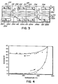
- Figure 3 is a side elevation view of a double edged tool with corner monitoring resistors for each of the cutting edges.
- Figure 4 is a curve of temperature versus resistance of a resistor suitable for use with the present invention.
- the tool 10 shown in Figure 1 has a rake face 12 and a plurality of flank faces 14, 16, 18 and 20 and has a cutting edge 22 defined by the intersection of the rake face 12 with the various flank faces 14, 16, 18 and 20.
- the tool will be made of material that does not distribute the heat generated by cutting uniformly rather the temperature of the tool immediately adjacent the portion of the cutting edge doing the cutting is generally significantly higher than the average temperature of the tool body.
- a corner thick film resistor 24 extends around each of the corners 26 defined by the intersections of pairs of adjacent faces 14, 16, 18 and 20 and is mounted on the faces 14, 16, 18 or 20.
- Preferably a pair of discrete thick film resistors 28 and 30 will be mounted on each of the faces 14, 16, 18 and 20 between the end of the corner resistors 24 applied to each of the faces.
- Each of the resistors 24, 28 and 30 is connected via conductors 32 and 34 to a conductor system 36 that separately connects each resistor 24, 28 and 30 to its respective terminals 38 on a face 14, 16, 18 or 20 other than the face on which the resistor is mounted (see Figure 3 for a typical wiring arrangement.)
- the corner resistors 24 each have both their conductors 32 and 34 connected to terminals on the same face 14, 16, 18 or 20 eg. the corner resistor 24 extending around the corner formed at the intersection of the faces 14 and 20 (selected resistor 24) may be connected to their respective terminals on face 16.
- the other resistor(s) 28 and 30 to be monitored at the same time as the selected resistor 24 will have their terminals 38 on the same face 16 as the terminals 38 for the selected resistor 24. Connecting the resistors to terminals 38 on an adjacent flank face facilitates connecting the resistors to a monitoring system when the tool is mounted in cutting position on the machine.
- the resistors 24, 28 and 30 are preferably positioned with their upper edges 40, i.e. the edge 40 adjacent to and substantially parallel to the adjacent portion of the cutting edge 22 of the tool. By so placing each of the edges 40 the resistors 24, 28 or 30 may be subjected to wear as the tool is worn to reduce the width w of the resistor 24, 28 or 30 which increases the resistance of the resistor by reducing the width of the conducting path which, as will be apparent, is dependent on the width and thickness of the thick film resistor 24.
- the thick film resistor 24 is preferably a substantially uniform thickness, uniform width conducting strip extending in a straight line along the flank face of the cutter such as flank faces 14, 16 as illustrated in Figure 1 (or equivalent faces 14A and 16A of Figure 3.)
- resistor 42 will be connected to suitable terminals not shown for measuring the resistance.
- the resistors 24, 28 and 30 could be embedded in the same manner as the resistor 42 but in the flank faces, however it is preferred to print the thick film resistors directly on the surface of the flank faces and then encapsulate them in a suitable dielectric layer 44 applied by printing and then firing.
- the conductors 32 and 34 and the cable 36 are similarly applied and encapsulated.
- the encapsulating material will normally be a glass material suitably loaded as desired.
- the resistors and their encapsulating layers may be applied to the faces 14, 16, 18 and 20 for example by screen printing.
- the ink used to form the thick film resistor 24 will be formulated to insure that the conducting phase of the resistor migrates to the interface between the resistor and the tool body as so locating the conducting portion 46 of the resistor (see Figure 2) will better protect the resistor from abrasive wear.
- the thick film resistor have the required properties, namely that when subjected to elevated temperatures (in the order of 300 - 500°C) the resistance of the resistor change significantly over time and that these changes be permanent changes so that the resistance of the resistor 24 may be measured at any time either on or off of the machine to determine the amount of thermal stress to which the tool 10 has been subjected thereby to provide an indication of the wear left in the tool.
- a double sided tool 10A having two rake faces 12A and 12B which define at their intersections with flank faces 14A, 16A (and 18A and 20A not shown) cutting edges 22A and 22B respectively.
- Corner resistors 124 and 124A (similar to resistor 24 of Figure 1) extend around the left most corner 26A adjacent the edges 22B and 22A respectively while similar resistors 224 and 224A extend around the central corner 26A and resistors 324 and 324A extend around the right hand corner 26A adjacent the edges 22B and 22A respectively of the tool 10A.
- Each of the resistors 124, 224, 324, 124A, 224A and 324A are connected to their monitoring terminals T equivalent to the terminals 38 of Figure 1 in the same manner.
- the resistor 124 is connected via lines 132 and 134 extending across the face 14A to terminals T2 located around the central corner 26A and on face 16A.
- the resistor 124A is similarly connected to terminals T 2A on face 16A by lines 132A and 134A.
- the resistors 224 and 224A are connected via lines 232, 234 and 232A and 234A respectively with terminals (on face 18A not shown), resistor 324 and 324A to further terminals (on face 20A not shown) and the resistors wrapping the corner of the tool 10A opposite the central corner 26A is connected to terminals T1 and T 1A .
- the resistance of the adjacent resistor is measured by connecting to terminals 38 (or T) either when the tool is in use on the machine or when the tool is removed from the machine.
- Figure 4 shows a typical curve of a resistance versus temperature.
- the 0's indicate increasing temperature and the boxes indicate decreasing temperatures.
- composition of the thick film resistor will be properly selected for the temperature conditions it will be required to monitor.
- the resistor 24, 124, 124A, 224, 224A etc., at the cutting corner is monitored to determine wear etc.
- the resistors 28 and 30 are not essential but when present it is preferred to monitor the resistors 28 and 30 on opposites sides of the corner resistor 24 being measured (for example if selected corner resistor 24 is the one on the left in Figure 1, the resistor 28 on face 14 and resistor 30 on face 20 (not shown) would be monitored). It is also practical to monitor the resistor 30 on face 14 at the same time or monitor only resistors 28 and 30 on face 14 and not resistor 30 on face 20 (assuming face 14 is the leading face.)
Landscapes
- Engineering & Computer Science (AREA)
- Mechanical Engineering (AREA)
- Cutting Tools, Boring Holders, And Turrets (AREA)
- Earth Drilling (AREA)
- Length Measuring Devices With Unspecified Measuring Means (AREA)
- Measurement Of Length, Angles, Or The Like Using Electric Or Magnetic Means (AREA)
- Machine Tool Sensing Apparatuses (AREA)
- Investigating Or Analyzing Materials By The Use Of Electric Means (AREA)
Claims (12)
- Ein Werkzeug mit einem Werkzeugkörper, der eine Schneidkante (22), die durch ein sich Kreuzen einer Freifläche (14, 16, 18, 20) und einer Spanfläche (12) des Werkzeugkörpers gebildet ist, und einen am Werkzeugkörper befestigten Widerstand (24) aufweist, gekennzeichnet durch
Befestigen des Widerstands (24) auf wärmeleitende Weise am Werkzeugkörper an einer Stelle des Werkzeugkörpers, die erhöhten Temperaturen ausgesetzt wird, die proportional zu erhöhten Temperaturen sind, denen ein Abschnitt der zu überwachenden Schneidkante (22) ausgesetzt ist, wobei der Widerstand (24) ein Widerstand der Art ist, dessen Widerstand sich bleibend im Verhältnis zu den Temperaturbedingungen und der Zeitdauer ändert, während der der Widerstand den Temperaturbedingungen ausgesetzt ist. - Werkzeug nach Anspruch 1, bei dem der Widerstand ein Dickfilmwiderstand ist.
- Werkzeug nach Anspruch 2, bei dem der Dickfilmwiderstand auf den Werkzeugkörper aufgebracht ist mit dem größeren Anteil einer leitenden Phase des Dickfilmwiderstands benachbart zu einer Grenzfläche des Widerstands und des Werkzeugkörpers.
- Werkzeug nach Anspruch 2, bei dem der Widerstand auf eine Freifläche des Werkzeugkörpers aufgebracht ist.
- Werkzeug nach Anspruch 4, bei dem der Widerstand ein geradliniger Widerstand mit einem im wesentlichen zur Schneidkante parallelen Rand ist, die durch die Freifläche gebildet ist, auf die der Widerstand aufgebracht ist.
- Werkzeug nach Anspruch 4, bei dem der Widerstand sich um eine Ecke erstreckt, die durch ein Paar angrenzender Freiflächen des Werkzeugs gebildet ist.
- Werkzeug nach Anspruch 4, bei dem eine leitende Phase des Widerstands angrenzend an die Freifläche angeordnet ist, auf die er aufgebracht ist, und bei dem der Widerstand in eine Schutzschicht gekapselt ist.
- Werkzeug nach Anspruch 4, bei dem der Widerstand angrenzend an die Schneidkante an einer Stelle angeordnet ist, die verschleißt, wenn die Kante ein bestimmtes Maß verschleißt, um den Stromleitpfad des Widerstands zu verringern und dadurch den Widerstand des Widerstands zum Anzeigen von Verschleiß an der Schneidkante zu erhöhen.
- Werkzeug nach Anspruch 7, bei dem der Widerstand angrenzend an die Schneidkante an einer Stelle angeordnet ist, die verschleißt, wenn die Kante ein bestimmtes Maß verschleißt, um den Stromleitpfad des Widerstands zu verringern und dadurch den Widerstand des Widerstands zum Anzeigen von Verschleiß an der Schneidkante zu erhöhen.
- Werkzeug nach Anspruch 2, bei dem der Widerstand in eine ausgewählte Fläche des Werkzeugs eingebettet ist.
- Verfahren zur Messung des Verschleißes eines Werkzeugs umfassend Aufbringen eines Widerstands auf den Körper des Werkzeugs und Messen des Widerstands des Widerstands, um eine Anzeige des Verschleißes zu liefern, dem ein überwachter Abschnitt der Schneidkante ausgesetzt worden ist, dadurch gekennzeichnet, daß das Aufbringen den Widerstand in wärmeleitender Weise angrenzend an den zu überwachenden Abschnitt aufbringt, so daß der Widerstand Temperaturbedingungen ausgesetzt ist, die proportional zu denen sind, denen der Abschnitt ausgesetzt ist, und wobei der Widerstand ein Widerstand der Art ist, dessen Widerstand im Verhältnis zu den erhöhten Temperaturbedingungen und der Zeitdauer bleibend geändert wird, während der der Widerstand den erhöhten Temperaturbedingungen ausgesetzt ist, so daß das Messen des Widerstands des Widerstands eine Anzeige der Temperaturbedingungen, denen der Abschnitt ausgesetzt war, und der Zeitdauer, in der der Abschnitt den erhöhten Temperaturbedingungen ausgesetzt war, und somit ein Maß für die verbleibende Werkzeugstandzeit in diesem Abschnitt liefert.
- Verfahren nach Anspruch 11, bei der Widerstand ein Dickfilmwiderstand ist.
Applications Claiming Priority (3)
| Application Number | Priority Date | Filing Date | Title |
|---|---|---|---|
| US497886 | 1990-03-23 | ||
| US07/497,886 US5000036A (en) | 1990-03-23 | 1990-03-23 | Tool wear detector |
| PCT/CA1991/000080 WO1991014924A1 (en) | 1990-03-23 | 1991-03-20 | Tool wear detector |
Publications (2)
| Publication Number | Publication Date |
|---|---|
| EP0521889A1 EP0521889A1 (de) | 1993-01-13 |
| EP0521889B1 true EP0521889B1 (de) | 1994-12-28 |
Family
ID=23978724
Family Applications (1)
| Application Number | Title | Priority Date | Filing Date |
|---|---|---|---|
| EP91905417A Expired - Lifetime EP0521889B1 (de) | 1990-03-23 | 1991-03-20 | Werkzeugabnützungsdetektor |
Country Status (7)
| Country | Link |
|---|---|
| US (1) | US5000036A (de) |
| EP (1) | EP0521889B1 (de) |
| JP (1) | JPH05505350A (de) |
| AT (1) | ATE116430T1 (de) |
| CA (1) | CA2077535A1 (de) |
| DE (1) | DE69106351T2 (de) |
| WO (1) | WO1991014924A1 (de) |
Families Citing this family (13)
| Publication number | Priority date | Publication date | Assignee | Title |
|---|---|---|---|---|
| SE460403B (sv) * | 1987-10-20 | 1989-10-09 | Birger Alvelid | Skaerverktyg foersett med tillstaandsgivare |
| DE4132454C2 (de) * | 1991-09-30 | 1994-07-21 | Bosch Gmbh Robert | Sägeblatt |
| WO1997049523A1 (en) * | 1996-06-26 | 1997-12-31 | The Gleason Works | Detecting tool wear by thermal monitoring of workpiece |
| US5861564A (en) * | 1997-09-26 | 1999-01-19 | Forintek Canada Corp. | Inspection bench with pivoting arm |
| US6526814B1 (en) * | 1999-09-29 | 2003-03-04 | Kyocera Corporation | Holder for throw-away tip with sensor |
| JP3359894B2 (ja) * | 1999-12-14 | 2002-12-24 | 京セラ株式会社 | 損耗センサ付きスローアウェイチップ |
| US6592303B2 (en) * | 2000-08-30 | 2003-07-15 | Kyocera Corporation | Throw-away tip |
| US7184515B2 (en) * | 2004-09-24 | 2007-02-27 | Battelle Memorial Institute | Component specific machine wear determination with x-ray fluorescence spectrometry |
| JP2008524006A (ja) * | 2004-12-20 | 2008-07-10 | レニショウ パブリック リミテッド カンパニー | 機械及び制御システム |
| US20090004449A1 (en) * | 2007-06-28 | 2009-01-01 | Zhigang Ban | Cutting insert with a wear-resistant coating scheme exhibiting wear indication and method of making the same |
| US8080323B2 (en) * | 2007-06-28 | 2011-12-20 | Kennametal Inc. | Cutting insert with a wear-resistant coating scheme exhibiting wear indication and method of making the same |
| US20170131710A1 (en) * | 2015-10-26 | 2017-05-11 | Caterpillar Inc. | Method and system for machine tool health early warning monitoring |
| CN105458312B (zh) * | 2015-12-14 | 2017-06-16 | 华中科技大学 | 一种微织构封装测温刀具 |
Family Cites Families (4)
| Publication number | Priority date | Publication date | Assignee | Title |
|---|---|---|---|---|
| DE247071C (de) * | ||||
| JPS54141472A (en) * | 1978-04-26 | 1979-11-02 | Fanuc Ltd | System for detecting tool abrasion |
| SE450352B (sv) * | 1985-11-07 | 1987-06-22 | Santrade Ltd | Sker med indikering av forslitning |
| US4757307A (en) * | 1986-08-04 | 1988-07-12 | General Electric Company | Tool condition sensing by measuring heat generation rate at the cutting edge |
-
1990
- 1990-03-23 US US07/497,886 patent/US5000036A/en not_active Expired - Fee Related
-
1991
- 1991-03-20 CA CA002077535A patent/CA2077535A1/en not_active Abandoned
- 1991-03-20 DE DE69106351T patent/DE69106351T2/de not_active Expired - Fee Related
- 1991-03-20 EP EP91905417A patent/EP0521889B1/de not_active Expired - Lifetime
- 1991-03-20 AT AT91905417T patent/ATE116430T1/de not_active IP Right Cessation
- 1991-03-20 WO PCT/CA1991/000080 patent/WO1991014924A1/en not_active Ceased
- 1991-03-20 JP JP91505265A patent/JPH05505350A/ja active Pending
Non-Patent Citations (1)
| Title |
|---|
| Bulletin of the Japan Society of Precision Engineering, vol. 21, no. 1, March 1987, Aoyama et al: "A study on a throw away tool equipped with a sensor to detect flank wear", pages 203-208 * |
Also Published As
| Publication number | Publication date |
|---|---|
| DE69106351D1 (de) | 1995-02-09 |
| WO1991014924A1 (en) | 1991-10-03 |
| US5000036A (en) | 1991-03-19 |
| CA2077535A1 (en) | 1991-09-24 |
| ATE116430T1 (de) | 1995-01-15 |
| JPH05505350A (ja) | 1993-08-12 |
| EP0521889A1 (de) | 1993-01-13 |
| DE69106351T2 (de) | 1995-05-18 |
Similar Documents
| Publication | Publication Date | Title |
|---|---|---|
| US5000036A (en) | Tool wear detector | |
| US4945770A (en) | State transducers in combination with mechanical components | |
| CA1320650C (en) | Brake block temperature and wear measuring device | |
| JPH03503862A (ja) | 状態インジケータを備えた切削工具 | |
| JP2972848B2 (ja) | 切削工具の摩耗量検出による工具寿命自動検知方法およびその装置 | |
| US5200698A (en) | System for sensing the position of a rotating steel shaft including a track formed by a strip having discontinuous electrical properties, and a method of manufacturing such a track | |
| EP0357203B1 (de) | Elektrische Leiter zur Engtoleranz-Bearbeitung | |
| US4041440A (en) | Method of adjusting resistance of a thick-film thermistor | |
| JPH06193660A (ja) | ブレーキライニングの厚さ及び温度同時検出用センサ | |
| CA2021004A1 (fr) | Carte a microcircuit protegee contre l'intrusion | |
| Scaramangas et al. | On the correction of residual stress measurements obtained using the centre‐hole method | |
| CN110788670B (zh) | 基于石墨烯传感器的刀具磨损监测系统 | |
| US4480376A (en) | Thermistors, their method of production | |
| JP3146353B2 (ja) | 損耗センサ付き切削工具 | |
| Briggs | Characterization of some chip resistors at low temperatures | |
| CN110788353B (zh) | 基于石墨烯传感器的切削刀片 | |
| JP2000135605A (ja) | 工具寿命センサ付き切削工具 | |
| JPH09109032A (ja) | サーモシールを貼り付けた乾式超砥粒ホイール | |
| RU2028587C1 (ru) | Тонкопленочный датчик давления | |
| GB2124789A (en) | Load measurement devices | |
| Berlicki et al. | Allowable power in NiCr film resistors | |
| Aoyania et al. | A Study on a Throw Away Tool Equipped with a Sensor to Detect Flank Wear | |
| KR100234192B1 (ko) | 박막자기헤드의 갭 깊이 제어용 전기적 래핑가이드 소자 | |
| JP2000094272A (ja) | 絶縁構造を有する損耗センサ付き切削工具 | |
| JPS6330752A (ja) | 機械部品表面の導線パタ−ン化加工による歪みや亀裂を感知する方法 |
Legal Events
| Date | Code | Title | Description |
|---|---|---|---|
| PUAI | Public reference made under article 153(3) epc to a published international application that has entered the european phase |
Free format text: ORIGINAL CODE: 0009012 |
|
| 17P | Request for examination filed |
Effective date: 19921019 |
|
| AK | Designated contracting states |
Kind code of ref document: A1 Designated state(s): AT BE CH DE DK ES FR GB GR IT LI LU NL SE |
|
| 17Q | First examination report despatched |
Effective date: 19931210 |
|
| GRAA | (expected) grant |
Free format text: ORIGINAL CODE: 0009210 |
|
| PG25 | Lapsed in a contracting state [announced via postgrant information from national office to epo] |
Ref country code: NL Effective date: 19941228 Ref country code: GR Free format text: LAPSE BECAUSE OF FAILURE TO SUBMIT A TRANSLATION OF THE DESCRIPTION OR TO PAY THE FEE WITHIN THE PRESCRIBED TIME-LIMIT Effective date: 19941228 Ref country code: ES Free format text: THE PATENT HAS BEEN ANNULLED BY A DECISION OF A NATIONAL AUTHORITY Effective date: 19941228 Ref country code: DK Effective date: 19941228 Ref country code: BE Effective date: 19941228 Ref country code: AT Effective date: 19941228 |
|
| REF | Corresponds to: |
Ref document number: 116430 Country of ref document: AT Date of ref document: 19950115 Kind code of ref document: T |
|
| ITF | It: translation for a ep patent filed | ||
| REF | Corresponds to: |
Ref document number: 69106351 Country of ref document: DE Date of ref document: 19950209 |
|
| ET | Fr: translation filed | ||
| PG25 | Lapsed in a contracting state [announced via postgrant information from national office to epo] |
Ref country code: SE Effective date: 19950328 |
|
| PG25 | Lapsed in a contracting state [announced via postgrant information from national office to epo] |
Ref country code: LU Free format text: LAPSE BECAUSE OF NON-PAYMENT OF DUE FEES Effective date: 19950331 |
|
| NLV1 | Nl: lapsed or annulled due to failure to fulfill the requirements of art. 29p and 29m of the patents act | ||
| PLBE | No opposition filed within time limit |
Free format text: ORIGINAL CODE: 0009261 |
|
| STAA | Information on the status of an ep patent application or granted ep patent |
Free format text: STATUS: NO OPPOSITION FILED WITHIN TIME LIMIT |
|
| 26N | No opposition filed | ||
| PGFP | Annual fee paid to national office [announced via postgrant information from national office to epo] |
Ref country code: GB Payment date: 19980316 Year of fee payment: 8 |
|
| PGFP | Annual fee paid to national office [announced via postgrant information from national office to epo] |
Ref country code: DE Payment date: 19980325 Year of fee payment: 8 |
|
| PGFP | Annual fee paid to national office [announced via postgrant information from national office to epo] |
Ref country code: FR Payment date: 19980326 Year of fee payment: 8 |
|
| PGFP | Annual fee paid to national office [announced via postgrant information from national office to epo] |
Ref country code: CH Payment date: 19980618 Year of fee payment: 8 |
|
| PG25 | Lapsed in a contracting state [announced via postgrant information from national office to epo] |
Ref country code: GB Free format text: LAPSE BECAUSE OF NON-PAYMENT OF DUE FEES Effective date: 19990320 |
|
| PG25 | Lapsed in a contracting state [announced via postgrant information from national office to epo] |
Ref country code: LI Free format text: LAPSE BECAUSE OF NON-PAYMENT OF DUE FEES Effective date: 19990331 Ref country code: CH Free format text: LAPSE BECAUSE OF NON-PAYMENT OF DUE FEES Effective date: 19990331 |
|
| GBPC | Gb: european patent ceased through non-payment of renewal fee |
Effective date: 19990320 |
|
| REG | Reference to a national code |
Ref country code: CH Ref legal event code: PL |
|
| PG25 | Lapsed in a contracting state [announced via postgrant information from national office to epo] |
Ref country code: FR Free format text: LAPSE BECAUSE OF NON-PAYMENT OF DUE FEES Effective date: 19991130 |
|
| REG | Reference to a national code |
Ref country code: FR Ref legal event code: ST |
|
| PG25 | Lapsed in a contracting state [announced via postgrant information from national office to epo] |
Ref country code: DE Free format text: LAPSE BECAUSE OF NON-PAYMENT OF DUE FEES Effective date: 20000101 |
|
| PG25 | Lapsed in a contracting state [announced via postgrant information from national office to epo] |
Ref country code: IT Free format text: LAPSE BECAUSE OF NON-PAYMENT OF DUE FEES;WARNING: LAPSES OF ITALIAN PATENTS WITH EFFECTIVE DATE BEFORE 2007 MAY HAVE OCCURRED AT ANY TIME BEFORE 2007. THE CORRECT EFFECTIVE DATE MAY BE DIFFERENT FROM THE ONE RECORDED. Effective date: 20050320 |