EP0522579A2 - Circuit de décalage de niveau pour circuits intégrés - Google Patents
Circuit de décalage de niveau pour circuits intégrés Download PDFInfo
- Publication number
- EP0522579A2 EP0522579A2 EP92111771A EP92111771A EP0522579A2 EP 0522579 A2 EP0522579 A2 EP 0522579A2 EP 92111771 A EP92111771 A EP 92111771A EP 92111771 A EP92111771 A EP 92111771A EP 0522579 A2 EP0522579 A2 EP 0522579A2
- Authority
- EP
- European Patent Office
- Prior art keywords
- transistor
- coupled
- doped region
- voltage
- doped
- Prior art date
- Legal status (The legal status is an assumption and is not a legal conclusion. Google has not performed a legal analysis and makes no representation as to the accuracy of the status listed.)
- Withdrawn
Links
- 230000005669 field effect Effects 0.000 claims abstract description 34
- 239000000758 substrate Substances 0.000 claims abstract description 26
- 238000002955 isolation Methods 0.000 abstract description 3
- 230000006870 function Effects 0.000 description 10
- 230000004044 response Effects 0.000 description 6
- 238000000034 method Methods 0.000 description 4
- 239000004065 semiconductor Substances 0.000 description 3
- 241000764773 Inna Species 0.000 description 2
- 238000003491 array Methods 0.000 description 2
- 238000005516 engineering process Methods 0.000 description 2
- 238000012986 modification Methods 0.000 description 2
- 230000004048 modification Effects 0.000 description 2
- 238000010586 diagram Methods 0.000 description 1
- 239000012212 insulator Substances 0.000 description 1
Images
Classifications
-
- H—ELECTRICITY
- H10—SEMICONDUCTOR DEVICES; ELECTRIC SOLID-STATE DEVICES NOT OTHERWISE PROVIDED FOR
- H10D—INORGANIC ELECTRIC SEMICONDUCTOR DEVICES
- H10D84/00—Integrated devices formed in or on semiconductor substrates that comprise only semiconducting layers, e.g. on Si wafers or on GaAs-on-Si wafers
- H10D84/80—Integrated devices formed in or on semiconductor substrates that comprise only semiconducting layers, e.g. on Si wafers or on GaAs-on-Si wafers characterised by the integration of at least one component covered by groups H10D12/00 or H10D30/00, e.g. integration of IGFETs
- H10D84/82—Integrated devices formed in or on semiconductor substrates that comprise only semiconducting layers, e.g. on Si wafers or on GaAs-on-Si wafers characterised by the integration of at least one component covered by groups H10D12/00 or H10D30/00, e.g. integration of IGFETs of only field-effect components
- H10D84/83—Integrated devices formed in or on semiconductor substrates that comprise only semiconducting layers, e.g. on Si wafers or on GaAs-on-Si wafers characterised by the integration of at least one component covered by groups H10D12/00 or H10D30/00, e.g. integration of IGFETs of only field-effect components of only insulated-gate FETs [IGFET]
- H10D84/85—Complementary IGFETs, e.g. CMOS
- H10D84/859—Complementary IGFETs, e.g. CMOS comprising both N-type and P-type wells, e.g. twin-tub
-
- H—ELECTRICITY
- H10—SEMICONDUCTOR DEVICES; ELECTRIC SOLID-STATE DEVICES NOT OTHERWISE PROVIDED FOR
- H10B—ELECTRONIC MEMORY DEVICES
- H10B41/00—Electrically erasable-and-programmable ROM [EEPROM] devices comprising floating gates
Definitions
- This invention relates to semiconductor memory devices and, more particularly, to field-effect transistor circuitry for using the supply and the reference voltages to switch a voltage higher than the supply voltage and to switch a negative voltage. Circuitry for shifting such positive and negative voltages is used, for example, in the row-line driver circuits of nonvolatile memory arrays, such as electrically-erasable, electrically-programmable, read-only-memory (EEPROM) arrays.
- EEPROM electrically-erasable, electrically-programmable, read-only-memory
- An EEPROM memory cell typically comprises a floating-gate field-effect transistor.
- the floating-gate of a programmed memory cell is charged with electrons, and the electrons in turn render the source-drain path under the charged floating gate nonconductive when a predetermined voltage is applied to the control gate.
- the nonconductive state is read by a sense amplifier as a "zero" bit.
- the floating-gate of a non-programmed cell is neutrally charged (or slightly positively or negatively charged) such that the source-drain path under the non-programmed floating gate is conductive when the predetermined voltage is applied to the control gate.
- the conductive state is read by a sense amplifier as a "one" bit.
- Each column and row of an EEPROM array may contain thousands of floating-gate memory cells.
- the sources of each cell in a column are connected to a source-column line and the source-column line for a selected cell may be connected to reference potential or ground during reading of the selected cell by a sense amplifier.
- the drains of each cell in a column are connected to a separate bitline (drain-column line).
- the control gates of each cell in a row are connected to a row line.
- the row line for a selected cell is connected by a row-line driver circuit to a voltage more positive than the supply voltage during programming of that cell.
- the row line for a selected cell is connected to a negative voltage during erasing of that cell.
- Field-effect transistor technology allows the generation of a negative voltage with respect to the circuit ground by using a voltage-multiplying technique.
- charge-pump circuits use only P-channel-type devices due to the necessity for insulating the generated negative voltage from the substrate, which is generally tied to the circuit ground.
- no N-channel-type transistors can be used in the negative voltage path since the N+/P- junction between the transistor source or drain and the substrate would be forward-biased for direct conduction, thus shorting the negative voltage to reference voltage Vss.
- circuits such as memory row-decoders, have been developed to switch a negative voltage.
- the implementation of those circuits has been difficult for a number of reasons.
- One of those reasons is a requirement for P-channel-type depletion transistors.
- a separate negative charge pump must be implemented for each node of the circuit, requiring an independent selection means for each charge pump.
- use of silicon-on-insulator technology is required. Where such circuits use P-channel-type only circuitry, a more negative voltage is required to control the switching.
- the field-effect transistor level-shifter of this invention selects and deselects a voltage Vp higher than supply voltage Vdd and a voltage Vn lower than reference voltage Vss using a deep N-tank to insulate the N-channel portions from the substrate.
- the circuit is formed on a substrate of first-conductivity-type coupled to reference voltage Vss.
- a first field-effect transistor has first and second N+ doped regions formed in a third isolating P- doped region. The third doped region is formed in a fourth isolating N- doped region, which is formed in the substrate.
- a second transistor has first and second N+ doped regions that may be formed in the same isolation regions as those of the first transistor.
- a third field-effect transistor has first and second P+ doped regions formed in an isolating N-region that is formed in the substrate.
- a fourth field-effect transistor has first and second N+ doped regions that may be formed in the same N- region as that of the third transistor.
- the gate of the first transistor is coupled to a first input.
- the first doped region of the first transistor is coupled to the output and the second doped region of the first transistor is coupled to the negative voltage Vn.
- the third doped region is coupled to the negative voltage Vn and the fourth doped region is coupled to the supply voltage Vdd.
- the gate of the second transistor is coupled to the output.
- the first doped region of the second transistor is coupled to the first input and the second doped region of the second transistor is coupled to the negative voltage Vn.
- the gate of the third transistor is coupled to the second input, which may be the same as the first input.
- the first doped region of the third transistor is coupled to the output and the second doped region of the third transistor is coupled to the voltage Vp, which is more positive than the supply voltage Vdd.
- the fifth doped region of the third transistor is also coupled to the voltage Vp.
- the gate of the fourth transistor is coupled to the output.
- the first doped region of the fourth transistor is coupled to the second input and the
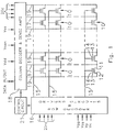
- Each EEPROM cell is a floating-gate transistor 10 having a source 11, a drain 12, a floating gate 13 and a control gate 14.
- Each of the control gates 14 in a row of cells 10 is connected to a row line 15, and each of the row lines 15 is connected to a row decoder 16, which includes row driver circuits.
- Each of the sources 11 in a column of cells 10 is connected to a source-column line 17, and each of the source-column lines 17 is connected to a column decoder 18, which includes at least one sense amplifier circuit.
- Each of the drains 12 in a column of cells 10 is connected to a drain-column line (bitline) 19, and each of the bitlines 19 is connected to the column decoder 18.
- the row decoder 16 may function, in response to row-line address signals on lines 20r and to a signal from control circuit 21, to place a preselected first programming voltage Vp (approx. +16 to +18 volts) on a selected row line 15, including a selected control-gate 14.
- Control circuit 21 may include a microprocessor separate from the memory chip.
- Column decoder 18, in response to signals on lines 20d and to a signal from control circuit 21, may function to place a preselected second programming voltage (reference potential Vss or ground, or a non-positive voltage) on selected source-column line 17, which includes a selected source region 11.
- the preselected second programming voltage Vss must differ sufficiently from the first preselected programming voltage Vp that excess electrons will migrate, perhaps by Fowler-Nordheim tunnelling, to the selected floating-gate 13 and, as a result, program that selected floating-gate 13.
- Column decoder 18 and row decoder 16 may optionally, in response to signals on lines 20d and 20r and in response to a signal from control circuit 21, place voltages of about +7 volts on deselected source-column lines 17 and/or on deselected row lines 15 to prevent a disturb of the programmed status of deselected cells 10.
- the floating gate 13 of the selected cell 10 is charged with electrons during programming, and the electrons in turn render the source-drain path under the floating gate 13 of the selected cell 10 nonconductive, a state which is read as a "zero" bit.
- Deselected cells 10 have source-drain paths under the floating gate 13 that remain conductive, and those cells 10 are read as "one" bits.
- the column decoder 18 may, for example, function to apply a positive voltage Vdd (approx. +5 volts) to the selected source-column line 17.
- the column decoder 18 may also, for example, function to leave at least the selected drain-column line 19 floating.
- the row decoder 16 may, for example, function to apply a high negative voltage Viii (approx. -11 volts) to the selected row line 15.
- the applied voltages function to remove excess electrons from the floating gate 13 of the a selected programmed cell 10.
- the row decoder 16 functions, in response to row-line address signals on lines 20r and to a signal from control circuit 21, to apply a preselected positive voltage (approx. +3 to +5 volts) to the selected row line 15 (and the selected control gate 14), and to apply a low voltage (ground or Vss) to deselected row lines 15.
- the column decoder 18 functions, in response to column address signals on lines 20d, to apply a preselected positive voltage Vsen (approx. +1 to +1.5 volts) to the selected drain-column line 19.
- the column decoder 18 also functions to connect all source-column lines 17 to ground (or Vss).
- the conductive or nonconductive state of the cell 10 connected to the selected drain-column line 19 and the selected row line 15 is detected by a sense amplifier, which supplies data to the DATA IN/OUT terminal.
- the source 11 regions and the drain 12 regions of the memory cells 10 may be interchanged for the various modes of operation.
- Fowler-Nordheim tunnelling for programming and/or erasing may take place between a drain 12 region and a floating-gate 13, or between a source 11 region and a floating-gate 13.
- Voltages applied to the source 11 and drain 12 regions in the read example above are interchangeable. Therefore, the terms "source” and “drain” as used herein are considered interchangeable for each mode of operation.
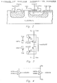
- FIG. 2 illustrates a deep N- tank configuration enclosing a P- tank in which an N-channel-type transistor is formed.
- the N-channel-type transistor is insulated from the substrate by the deep N- tank connected to a supply voltage Vdd and, therefore, the applied voltage Vn can be lower than reference voltage Vss, thus making possible the selection of a negative voltage Vn.
- the P-channel-type transistor is insulated from the substrate by a relatively shallow N- tank. That N- tank allows a voltage Vp to be applied to a source-drain region of the P-channel-type transistor where that voltage Vp is greater in magnitude than the supply voltage Vdd.
- the level-shifter circuit illustrated has a supply voltage Vdd, a reference voltage Vss, a negative voltage Vn, a voltage Vp more positive than the supply voltage Vdd, a first input INN, a second input INP (which may be the same as the first input INN) and an output OUT.
- the circuit is formed on a substrate of first-conductivity-type coupled to reference voltage Vss.
- a first field-effect transistor N1 has first and second doped regions N+ of a second conductivity-type formed in a third doped region P- of first conductivity-type.
- the third doped region P- of the first transistor N1 is formed in a fourth doped region N- of second conductivity-type and the fourth doped region N- of the first transistor is formed in the SUBSTRATE as illustrated in FIG. 2.
- a second field-effect transistor N2 also has first and second doped regions of the second conductivity-type and the first and second doped regions are also formed in a third doped region of first conductivity-type.
- the third doped region of the second transistor is also formed in the fourth doped region of second conductivity-type.
- a third field-effect transistor P1 has first and second doped regions P+ of first conductivity-type formed in a fifth doped region N- of second conductivity-type.
- the fifth doped region N- is formed in the SUBSTRATE as illustrated in FIG. 2.
- a fourth field-effect transistor P2 also has first and second doped regions of first conductivity-type formed in a fifth doped region of second conductivity-type.
- a fifth field-effect transistor of second conductivity-type has a gate and a source-drain path.
- the gate of the fifth transistor is coupled to the reference voltage and the source-drain path of the fifth transistor is coupled between the first input INN and the gate of the first field-effect transistor N1.
- a sixth field-effect transistor of first conductivity-type has a gate and a source-drain path.
- the gate of the sixth transistor N3 is coupled to the supply voltage Vdd and the source-drain path of the sixth transistor N3 is coupled between the second input INP, and/or the first input INN, and the gate of the third field-effect transistor P1.
- the first transistor has a channel region CH1 between the first and second doped regions, has a gate NGATE insulated from the channel region.
- the gate NGATE of the first transistor is coupled to the first input INN.
- the first doped region N+ of the first transistor is coupled to the output OUT and the second doped region N+ of the first transistor is coupled to the negative voltage Vn.
- the third doped region P- is coupled to the negative voltage Vn and the fourth doped region N- is coupled to the supply voltage Vdd.
- the second transistor N2 has a channel region between first and second doped regions and has a gate insulated from the channel region.
- the gate of the second transistor N2 is coupled to the output OUT.
- the first doped region of the second transistor N2 is coupled to the first input INN and the second doped region of the second transistor N2 is coupled to the negative voltage Vn.
- the third transistor P1 has a channel region CH2 between the first and second doped regions P+ and has a gate PGATE insulated from the channel region CH2.
- the gate of the third transistor P1 is coupled to the second input INP (and/or the first input INN).
- the first doped region P+ of the third transistor P1 is coupled to the output OUT and the second doped region P+ of the third transistor is coupled to the voltage Vp, which is more positive than the supply voltage Vdd.
- the fifth doped region N- of the third transistor is also coupled to the voltage Vp.
- the fourth transistor P2 has a channel region between first and second doped regions and has a gate insulated from the channel region.
- the gate of the fourth transistor P2 is coupled to the output OUT.
- the first doped region of the fourth transistor P2 is coupled to the second input INP (which may be the same as the first input INN) and the second doped region of the fourth transistor P2 is coupled to the voltage Vp.
- the first conductivity-type may be P-type and one of either the supply voltage Vdd or the reference voltage Vss may be coupled to the input terminals INP and INN.
- the circuit of FIG. 3 operates as a field-effect-transistor inverter.
- transistor P1 When the INP and INN terminals are at Vdd, transistor P1 is nonconductive, transistor N1 is conductive and, therefore, the output terminal OUT is at Vss.
- the feedback transistor P2 restores the full Vdd level on the PGATE terminal.
- transistor P1 When the INP and INN terminals are at Vss, transistor P1 is conductive and transistor N1 is nonconductive and, therefore, the output terminal OUT is at supply voltage Vdd.
- the feedback transistor N2 restores the full reference voltage Vss level on the NGATE terminal to ensure that transistor N1 is nonconductive.
- Vn lower than reference voltage Vss the supply voltage Vdd level is applied to terminals INP and INN.
- the negative voltage Vn may be lowered from Vss and the voltage at the output terminal OUT will follow the applied voltage negative voltage Vn.
- each of the circuits A and B of FIG. 4 may be identical to the circuit of FIG. 3.
- Circuit A operates as explained in the previous section in which the operation of the circuit of FIG. 3 was discussed.
- Transistor N1 is conductive and, therefore, terminal OUTB is at voltage level Vss.
- Feedback transistor P2 is conductive and raises the voltage at PGATE to Vp, thus causing transistor P1 to be nonconductive and, therefore, the charge pump circuit driving the Vp terminal will not be loaded by direct current.
- Transistor N3 is nonconductive and, therefore, the voltage source Vp is insulated from the circuit driving INPB and INNB.
- Transistor P1 is conductive and, therefore, terminal OUTB is at supply voltage Vdd.
- Feedback transistor N2 is conductive and, therefore, terminal NGATE is lowered to Vn. Therefore, transistor N1 is nonconductive and the charge pump driving Vn is not loaded by direct current.
- Transistor P3 is nonconductive and, therefore, voltage Vn is insulated from the circuit driving terminals INPB and INNB.
- the field-effect-transistor circuit of this invention may be formed on a substrate that is biased to Vss, yet the circuit is able to select and deselect voltages higher than circuit supply voltage Vdd and lower than reference voltage Vss.
Landscapes
- Read Only Memory (AREA)
- Semiconductor Memories (AREA)
Applications Claiming Priority (2)
| Application Number | Priority Date | Filing Date | Title |
|---|---|---|---|
| US07/728,928 US5157281A (en) | 1991-07-12 | 1991-07-12 | Level-shifter circuit for integrated circuits |
| US728928 | 1991-07-12 |
Publications (2)
| Publication Number | Publication Date |
|---|---|
| EP0522579A2 true EP0522579A2 (fr) | 1993-01-13 |
| EP0522579A3 EP0522579A3 (en) | 1994-07-20 |
Family
ID=24928846
Family Applications (1)
| Application Number | Title | Priority Date | Filing Date |
|---|---|---|---|
| EP19920111771 Withdrawn EP0522579A3 (en) | 1991-07-12 | 1992-07-10 | Level-shifter circuit for integrated circuits |
Country Status (3)
| Country | Link |
|---|---|
| US (1) | US5157281A (fr) |
| EP (1) | EP0522579A3 (fr) |
| JP (1) | JPH05250888A (fr) |
Cited By (2)
| Publication number | Priority date | Publication date | Assignee | Title |
|---|---|---|---|---|
| WO2000016399A1 (fr) * | 1998-09-10 | 2000-03-23 | Infineon Technologies Ag | Circuit a semiconducteur |
| WO2000057475A1 (fr) * | 1999-03-23 | 2000-09-28 | Infineon Technologies Ag | Circuit integre comportant deux transistors presentant des types de conduction differents |
Families Citing this family (23)
| Publication number | Priority date | Publication date | Assignee | Title |
|---|---|---|---|---|
| JP3094469B2 (ja) * | 1991-01-18 | 2000-10-03 | ソニー株式会社 | 出力バッファ回路 |
| JP2835215B2 (ja) * | 1991-07-25 | 1998-12-14 | 株式会社東芝 | 不揮発性半導体記憶装置 |
| EP0954102A1 (fr) * | 1991-12-09 | 1999-11-03 | Fujitsu Limited | Porte OU/NON-OU exclusif |
| US5243236A (en) * | 1991-12-31 | 1993-09-07 | Intel Corporation | High voltage CMOS switch with protection against diffusion to well reverse junction breakdown |
| KR940003026A (ko) * | 1992-07-13 | 1994-02-19 | 김광호 | 트리플웰을 이용한 반도체장치 |
| US5371419A (en) * | 1992-11-23 | 1994-12-06 | Mitsubishi Denki Kabushiki Kaisha | CMOS well switching circuit |
| JP2978346B2 (ja) * | 1992-11-30 | 1999-11-15 | 三菱電機株式会社 | 半導体集積回路装置の入力回路 |
| US5300835A (en) * | 1993-02-10 | 1994-04-05 | Cirrus Logic, Inc. | CMOS low power mixed voltage bidirectional I/O buffer |
| US5440244A (en) * | 1993-02-10 | 1995-08-08 | Cirrus Logic, Inc. | Method and apparatus for controlling a mixed voltage interface in a multivoltage system |
| JPH06314773A (ja) * | 1993-03-03 | 1994-11-08 | Nec Corp | 半導体装置 |
| US5355032A (en) * | 1993-03-24 | 1994-10-11 | Sun Microsystems, Inc. | TTL to CMOS translator circuit and method |
| US5515319A (en) * | 1993-10-12 | 1996-05-07 | Texas Instruments Incorporated | Non-volatile memory cell and level shifter |
| JP3623004B2 (ja) * | 1994-03-30 | 2005-02-23 | 松下電器産業株式会社 | 電圧レベル変換回路 |
| US5450357A (en) * | 1994-04-01 | 1995-09-12 | Texas Instruments Incorporated | Level shifter circuit |
| EP0738011B1 (fr) | 1995-04-12 | 2014-12-10 | Fuji Electric Co., Ltd. | Circuit intégré à haute tension, structure de terminaison de jonction à haute tension et transistor MIS à haute tension |
| JP3068513B2 (ja) * | 1997-07-04 | 2000-07-24 | 日本電気株式会社 | 半導体装置、その製造方法 |
| US6303438B1 (en) * | 1998-02-02 | 2001-10-16 | Matsushita Electric Industrial Co., Ltd. | Method for manufacturing a nonvolatile semiconductor memory device having increased hot electron injection efficiency |
| US6384643B1 (en) * | 1999-12-16 | 2002-05-07 | Texas Instruments Incorporated | Temperature and process compensated LDMOS drain-source voltage |
| EP1139567B1 (fr) * | 2000-03-27 | 2006-02-08 | Kabushiki Kaisha Toshiba | Circuit de conversion de niveau |
| US6995598B2 (en) * | 2003-02-13 | 2006-02-07 | Texas Instruments Incorporated | Level shifter circuit including a set/reset circuit |
| US20070063758A1 (en) * | 2005-09-22 | 2007-03-22 | Honeywell International Inc. | Voltage divider and method for minimizing higher than rated voltages |
| US7447085B2 (en) * | 2006-08-15 | 2008-11-04 | Micron Technology, Inc. | Multilevel driver |
| US7770641B2 (en) * | 2007-12-18 | 2010-08-10 | Chevron U.S.A. Inc. | Method for enhancing oil recovery with an improved oil recovery surfactant |
Family Cites Families (8)
| Publication number | Priority date | Publication date | Assignee | Title |
|---|---|---|---|---|
| US5066995A (en) * | 1987-03-13 | 1991-11-19 | Harris Corporation | Double level conductor structure |
| US5061981A (en) * | 1987-05-22 | 1991-10-29 | Hall John H | Double diffused CMOS with Schottky to drain contacts |
| US5060044A (en) * | 1987-05-28 | 1991-10-22 | Texas Instruments Incorporated | Integrated bipolar-CMOS circuit isolation for providing different backgate and substrate bias |
| JPS6410656A (en) * | 1987-07-03 | 1989-01-13 | Hitachi Ltd | Complementary type semiconductor device |
| US4812891A (en) * | 1987-12-17 | 1989-03-14 | Maxim Integrated Products | Bipolar lateral pass-transistor for CMOS circuits |
| DE3900769A1 (de) * | 1989-01-12 | 1990-08-09 | Fraunhofer Ges Forschung | Integrierte schaltung mit zumindest einem n-kanal-fet und zumindest einem p-kanal-fet |
| IT1228900B (it) * | 1989-02-27 | 1991-07-09 | Sgs Thomson Microelectronics | Struttura integrata monolitica per sistema di pilotaggio a due stadi con componente circuitale traslatore di livello del segnale di pilotaggio per transistori di potenza. |
| IT1235843B (it) * | 1989-06-14 | 1992-11-03 | Sgs Thomson Microelectronics | Dispositivo integrato contenente strutture di potenza formate con transistori ldmos complementari, strutture cmos e pnp verticali con aumentata capacita' di supportare un'alta tensione di alimentazione. |
-
1991
- 1991-07-12 US US07/728,928 patent/US5157281A/en not_active Expired - Lifetime
-
1992
- 1992-07-10 EP EP19920111771 patent/EP0522579A3/en not_active Withdrawn
- 1992-07-13 JP JP22775492A patent/JPH05250888A/ja active Pending
Cited By (3)
| Publication number | Priority date | Publication date | Assignee | Title |
|---|---|---|---|---|
| WO2000016399A1 (fr) * | 1998-09-10 | 2000-03-23 | Infineon Technologies Ag | Circuit a semiconducteur |
| US6480044B2 (en) | 1998-09-10 | 2002-11-12 | Infineon Technologies Ag | Semiconductor circuit configuration |
| WO2000057475A1 (fr) * | 1999-03-23 | 2000-09-28 | Infineon Technologies Ag | Circuit integre comportant deux transistors presentant des types de conduction differents |
Also Published As
| Publication number | Publication date |
|---|---|
| JPH05250888A (ja) | 1993-09-28 |
| EP0522579A3 (en) | 1994-07-20 |
| US5157281A (en) | 1992-10-20 |
Similar Documents
| Publication | Publication Date | Title |
|---|---|---|
| US5157281A (en) | Level-shifter circuit for integrated circuits | |
| US5412603A (en) | Method and circuitry for programming floating-gate memory cell using a single low-voltage supply | |
| US8130589B2 (en) | Semiconductor memory device using only single-channel transistor to apply voltage to selected word line | |
| US5796656A (en) | Row decoder circuit for PMOS non-volatile memory cell which uses electron tunneling for programming and erasing | |
| US7209392B2 (en) | Single poly non-volatile memory | |
| EP0467928B1 (fr) | Cellules de memoire vive non volatile amelioree utilisant deux elements differentiels de memoire non volatile pouvant etre desaccouples | |
| US6373749B1 (en) | Channel-erase nonvolatile semiconductor memory device | |
| US6429724B1 (en) | Semiconductor device capable of generating a plurality of voltages | |
| EP0320916B1 (fr) | Mémoire morte électriquement effaçable et programmable utilisant des cellules à portes empilées | |
| EP0374936B1 (fr) | Systéme de mémoire non volatile à semi-conducteurs | |
| EP0499110A2 (fr) | Commutateur pour utilisation dans un circuit intégré | |
| US6243292B1 (en) | Nonvolatile semiconductor memory device capable of reducing memory array area | |
| US5287536A (en) | Nonvolatile memory array wordline driver circuit with voltage translator circuit | |
| US6291862B1 (en) | Supply voltage reduction circuit for integrated circuit | |
| US6819597B2 (en) | Row decoder in flash memory and erase method of flash memory cell using the same | |
| US6049498A (en) | Double transistor switch for supplying multiple voltages to flash memory wordlines | |
| US5295113A (en) | Flash memory source inhibit generator | |
| US8174884B2 (en) | Low power, single poly EEPROM cell with voltage divider | |
| EP0453812B1 (fr) | Circuit d'attaque de ligne de mot pour réseau de cellule de mémoire non volatile | |
| US20080031051A1 (en) | Memory device and method for programming a nonvolatile memory matrix |
Legal Events
| Date | Code | Title | Description |
|---|---|---|---|
| PUAI | Public reference made under article 153(3) epc to a published international application that has entered the european phase |
Free format text: ORIGINAL CODE: 0009012 |
|
| AK | Designated contracting states |
Kind code of ref document: A2 Designated state(s): DE FR GB IT NL |
|
| PUAL | Search report despatched |
Free format text: ORIGINAL CODE: 0009013 |
|
| AK | Designated contracting states |
Kind code of ref document: A3 Designated state(s): DE FR GB IT NL |
|
| 17P | Request for examination filed |
Effective date: 19950207 |
|
| 17Q | First examination report despatched |
Effective date: 19961009 |
|
| STAA | Information on the status of an ep patent application or granted ep patent |
Free format text: STATUS: THE APPLICATION IS DEEMED TO BE WITHDRAWN |
|
| 18D | Application deemed to be withdrawn |
Effective date: 19970422 |