EP0523627A2 - Unité de commande programmable pour plusieurs unités centrales de traitement - Google Patents
Unité de commande programmable pour plusieurs unités centrales de traitement Download PDFInfo
- Publication number
- EP0523627A2 EP0523627A2 EP92111983A EP92111983A EP0523627A2 EP 0523627 A2 EP0523627 A2 EP 0523627A2 EP 92111983 A EP92111983 A EP 92111983A EP 92111983 A EP92111983 A EP 92111983A EP 0523627 A2 EP0523627 A2 EP 0523627A2
- Authority
- EP
- European Patent Office
- Prior art keywords
- controller
- units
- bus
- access
- unit
- Prior art date
- Legal status (The legal status is an assumption and is not a legal conclusion. Google has not performed a legal analysis and makes no representation as to the accuracy of the status listed.)
- Withdrawn
Links
Images








Classifications
-
- G—PHYSICS
- G06—COMPUTING OR CALCULATING; COUNTING
- G06F—ELECTRIC DIGITAL DATA PROCESSING
- G06F15/00—Digital computers in general; Data processing equipment in general
- G06F15/16—Combinations of two or more digital computers each having at least an arithmetic unit, a program unit and a register, e.g. for a simultaneous processing of several programs
-
- G—PHYSICS
- G06—COMPUTING OR CALCULATING; COUNTING
- G06F—ELECTRIC DIGITAL DATA PROCESSING
- G06F13/00—Interconnection of, or transfer of information or other signals between, memories, input/output devices or central processing units
- G06F13/14—Handling requests for interconnection or transfer
- G06F13/36—Handling requests for interconnection or transfer for access to common bus or bus system
- G06F13/362—Handling requests for interconnection or transfer for access to common bus or bus system with centralised access control
Definitions
- the present invention is directed to a multi-CPU programmable controller, and more particularly to such programmable controller having two or more controller unit including individual CPUs which operate independently from each other to access one of a plurality of I/O interface units through a common I/O bus for controlling the associated one of equipments connected respectively to the I/O interface units.
- a multi-CPU Programmable controller having two or more CPUs already known in the art is designed to include a master controller unit with a master CPU [referred to as master CPU unit] and one or more slave CPU controller units with individual slave CPUs [referred to as salve CPU unit].
- master CPU unit in made responsible for managing to operate a plurality of I/O interface units over the slave CPU unit or units for controlling equipments or control devices connected respectively to the I/O interface units. For example, when activating the equipments, the master CPU unit collects data from the slave CPU unit or units through a common memory for operating the I/O interface units based upon thus collected date.
- the master CPU unit When, on the other hand, making data-input to the master and slave CPU units, the master CPU unit is also made responsible for collecting data respectively from the individual equipments through the I/O interface unit and distributing the data to the slave CPU units through the common memory. In this prior system, therefore, the slave CPU unit is not allowed to control the I/O interface units or the associated equipments independently of the master CPU unit. Consequently, the prior system suffers from the following drawbacks.
- Another programmable controller with two controller units with individual CPUs in which the two controller units operate alternately as a master CPU unit and a slave CPU unit for controlling a plurality of I/O interface units and corresponding equipments or control devices connected thereto through a common I/O bus.
- the slave CPU unit is required to monitor the master CPU unit accessing the I/O interface unit in order to take over and access instead the corresponding I/O interface unit through the common I/O bus. This is possible only with a software monitoring the status of the CPU units and therefore suffers from a loss time in arbitration between the CPU units.
- the multi-CPU programmable controller in accordance with the present invention operates to access one of a plurality of I/O interface units through a common I/O bus for controlling one of a plurality of equipments or control devices connected to the I/O interface units.
- the system comprises a pair of controller units with individual CPUs which operate in accordance with specific programs independently from each other such that each controller unit generates an access signal to access one of the I/O units for controlling the associated equipment within one bus cycle.
- the controller units, I/O bus and I/O units are mounted on a single base board.
- the board includes a bus arbitrator having a sampling clock and supervising access signals from the two controller units to determine based upon a timing of the sampling clock which of the controller units is first to generate the access signal when the access signals are received within the one bus cycle from the two controller units, thereby giving priority to one of the two controller units over the other and assuming the one controller units as a prior controller unit and the other controller unit as a posterior controller unit.
- the bus arbitrator allows to the prior controller unit to use the common I/O bus and access corresponding one of the I/O interface units while giving a hardware-wait signal in order to stall the posterior controller unit so long as the posterior controller unit generates the access signal within the bus cycle during which the prior controller units continues to access the corresponding I/O interface unit, and allows the posterior controller unit to use the common I/O bus and access a corresponding I/O interface unit upon completion of the access from the prior controller unit to the corresponding I/O interface unit.
- two of the controller units can operates substantially independently from each other in a sense that one of the controller units does not require to interact with the other controller units but simply follows sequence order determined by the bus arbitrator.
- the bus arbitrator is designed to generate two sampling clocks of different phases for judging the on-coming access signals from the two controller units respectively at the different timings defined by the out-of-phase sampling clocks. With this scheme, the bus arbitrator can acknowledge no concurrent access signals from the two controller units within the one bus cycle, therefore successfully avoiding the contention between the two controller units in judging priority therebetween.
- the base board is formed with first and second slots for receiving therein the controller units, respectively, and is also provided with an I/O interface unit allocator.
- the allocator includes means for correlating the first and second slots respectively with the two controller units, and means for setting common and exclusive use data for each one of the I/O interface units.
- common use data is meant that the corresponding I/O interface unit is commonly controlled by the two controller unit
- exclusive use data is meant that the corresponding I/O interface unit is exclusively controlled by one of the controller units which is correlated with a particular one of the slots.
- interlocking is made simply by a hardware scheme so that the system can be free from the rather complicated user defined software or program. Further, because of such hardware interlocking between the I/O interface units and the controller units, the I/O interface unit exclusively interlocked to the one controller units can not well prevented from receiving error signal, for example, initialization signal which should be directed to the other I/O interface unit or units, whereby the I/O interface units can be safely controlled.
- the system utilizes a common memory in the form of a dual-port RAM which is provided exteriorly or separately of the controller units and is interconnected to internal memories respectively within the controller units.
- the internal memory of each controller unit is configured to have a particular exchange data area for storing data to be exchanged between the controller units through the dual-port RAM under the control of the controller unit, so that the data stored in the particular exchange data area in the internal memory of each one of the controller units can be automatically transferred through the common memory, i.e., dual-port RAM to the exchange data area in the internal memory of the other controller unit without requiring no additional user defined program for control of the dual-port RAM.
- each of the controller units is designed to have an instruction which designates specific location in the internal memory of each one of the controller units for transferring data specified by that location between the internal memories through the dual-port RAM. Also, in this scheme, such instruction can be made executed internally in accordance with the user defined program for control of the I/O interface units without requiring no additional particular user program for control of the dual-port RAM.
- the present invention discloses a further advantageous feature for a system configuration in which three or more controller units each including a CPU are cooperative to control a plurality of the I/O interface units through the common I/O bus.
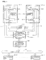
- a multi-CPU programmable controller in accordance with a preferred embodiment of the present invention includes a pair of controller units 10-1 and 10-2 each including a CPU, wait controller W1 , W2 , internal memory M1 , M2 and a buffer B1 , B2 .
- the controller units 10-1 and 10-2 are connected through a common I/O bus 20 to a plurality of I/O interface units 30-0 to 30-7 for controlling equipments or control devices wired respectively to the I/O interface units 30-0 to 30-7 .
- the control by the controller units 10-1 and 10-2 are made substantially independently from each other in accordance with particular programs for the individual CPUs.
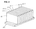
- the controller units 10-1 and 10-2 are presented into modular packages mounted on a base board 40 , as shown in FIG. 2, together with the I/O interface units 30-0 to 30-7 and a power unit 41 for energization of the controller system.
- the base board 40 is provided with a common memory CM disposed exteriorly of the controller units for exchanging data between the internal memories M1 and M2 of the controller units 10-1 and 10-2 .
- the base board 40 is also provided with a bus arbitrator 50 and an I/O interface unit allocator 80 .
- the I/O interface unit allocator 80 is provided to correlate the individual I/O interface units 30-0 to 30-7 with the controller units 10-1 and 10-2 such that each I/O interface unit is set to be controlled exclusively by one of the controller units or commonly by the two controller units 10-1 and 10-2 , the detail of which will be discussed later.
- Each of the CPUs produces a bus access signal through the corresponding one of the buffers B1 and B2 and through a local I/O bus 1-1 , 1-2 to the bus arbitrator 50 during the execution of controlling the corresponding I/O interface unit or units, or one bus cycle determined at the wait controller W1 , W2 for that execution.
- the bus arbitrator 50 is provided to determine priority between the controller units 10-1 and 10-2 or the CPUs thereof in controlling the I/O interface units 30-0 to 30-7 , when it is recognized that one of the controller units 10-1 and 10-2 produces the bus access signal while the other controller unit produces the bus access signal, or during the bus cycle of the other controller unit executing the operation of controlling the I/O interface unit or units.
- the bus arbitrator 50 is composed of a bus selector 60 and a wait controller 70 . It is the bus selector 60 that determines the priority between the controller units 10-1 and 10-2 by supervising the bus access signals I/OC81 and I/OC82 respectively from the CPUs of the controller units 10-1 and 10-2 , and provide bus select signals BUSEN1 and BUSEN2 indicative of that the controller units 10-1 and 10-2 are enabled to access the corresponding I/O interface unit through the common I/O bus 20 .
- the wait controller 70 is provided to output wait signal WAIT1 and WAIT2 to the wait controller W1 and W2 of the controller units 10-1 and 10-2 , respectively.
- the wait signal WAIT1 and WAIT2 are responsible for deferring the access of the controller units 10-1 and 10-2 to the common I/O bus 20 and are also cooperative with the bus select signals BUSEN1 and BUSEN2 from the bus selector 60 , respectively in order to give a sufficient time frame for the CPU of the controller units in accessing the common I/O bus 20 , such that only one of the two controller units is allowed to access the I/O bus 20 while inhibiting the other controller unit from accessing the I/O bus 20 when the bus access signals I/OCS1 and I/OCS2 are recognized within one bus cycle of the controller unit 10-1 or 10-2 .
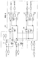
- FIG. 4 illustrates a schematic circuit diagram of the bus selector 60 which includes a pair of D-type flip-flops 61 and 62 receiving the inputs of the bus access signals I/OCS1 and I/OCS2 respectively together with the sampling clock CLK, a logic circuit 63 for determination of the priority, and a pair of D-type flip-flops 64 and 65 which output the bus select signal BUSEN1 and BUSEN2 , respectively.
- the logic circuit 63 is designed to satisfy a logic table listed in the below:
- the sampling clock CLK provides a basis for the determination of the priority of the bus access signal I/OCS1 and I/OCS2 . That is, any one of I/OCS1 and I/OCS2 that is received in a preceding cycle of the sampling clock CLK is given priority over the other which is received in a succeeding cycle of CLK.
- the bus selector 60 in response to this simultaneous occurrence of the signals, selects one of the controller units, in this instance, the unit 10-1 as a prior unit which is preselected to be given priority to the other.
- the bus selector 60 produces the bus select signal BUSEN1 which allows the controller unit 10-1 to access the corresponding I/O interface unit or units through the common I/O bus 20 .
- Condition nos. 4 , 5 , and 6 indicate contention in which one of the bus access signals I/OCS1 and I/OCS2 from the corresponding one of the controller units 10-1 and 10-2 is received during the one bus cycle of the other controller unit.
- the wait controller 70 responds to produce the wait signal WAIT1 and WAIT2 to the corresponding one of the controller units 10-1 and 10-2 in order to defer the access thereof to the common I/O bus 20 until the other controller unit, i.e., the prior controller unit completes its bus cycle of completing the access to the common I/O bus 20 .
- the other controller unit Upon completion of the control by the prior controller unit, the other controller unit is enabled to access to the common I/O bus 20 for controlling the corresponding I/O interface unit or units.
- the bus select signal BUSEN1 and BUSEN2 are produced from the bus selector 60 when the following relations are satisfied.
- BUSEN1 (I/OCS1 ⁇ I/OCS2 ⁇ ) No. 2 ⁇ (I/OCS1 ⁇ I/OCS2) ⁇ ( BUSEN1 ⁇ t-1 ⁇ BUSEN1 ⁇ t-1 ) No. 4 ⁇ (I/OCS1 ⁇ I/OCS2) ⁇ (BUSEN1 t-1 ) No. 5
- BUSEN2 ( I/OCS1 ⁇ ⁇ I/OCS2) No. 3 ⁇ (I/OCS1 ⁇ I/OCS2) ⁇ (BUSEN1 t-1 ) No.
- the wait controller 70 of the bus arbitrator 50 operates to produce the wait signals WAIT1 and WAIT2 .
- the wait signals WAIT1 and WAIT2 are defined such that the wait controller 11-1 and 11-2 in the controller units 10-1 and 10-2 are authorized to determine the bus cycle of the individual CPUs for accessing the common I/O bus 20 when the wait signal WAIT1 and WAIT2 to the wait controllers 11-1 and 11-2 are at high level and that wait controller 70 of the bus arbitrator 50 takes over to determine the bus cycle of the CPUs of the respective controller units 10-1 and 10-2 when the wait signal WAIT1 and WAIT2 are at low levels [ WAIT1 ⁇ and WAIT2 ⁇ ].
- the bus arbitrator 50 responds to stall the CPU in one of the controller units 10-1 and 10-2 producing the bus access signal later until the CPU of the other controller unit completes the access to the I/O bus, which is acknowledged on the side of the bus arbitrator 50 by BUSEN1 or BUSEN2 . Thereafter, the bus arbitrator 50 still keep producing low level WAIT1 ⁇ or WAIT2 ⁇ for a certain period determined by the wait controller 70 sufficient for completing the access to the I/O bus. Subsequently, the bus arbitrator 50 responds to again produce high level WAIT1 and WAIT2 so that the wait controllers 11-1 and 11-2 takes over.
- the wait signals WAIT1 and WAIT2 are produced when the following relations are satisfied.
- WAIT1 I/OCS1 ⁇ I/OCS2 ⁇ BUSEN2 t-1
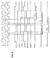
- WAIT2 (I/OCS1 ⁇ I/OCS2) ⁇ ⁇ (BUSEN1 t-1 ⁇ BUSEN2 t-1 ) ⁇ (BUSEN1 t-1 ) ⁇ Operation of the bus arbitrator 50 is now explained with reference to the timing chart of FIG. 5 illustrating one example which includes the following three consecutive stages:
- the bus arbitrator 50 produces BUSEN1 and BUSEN2 ⁇ , while keeping WAIT1 and WAIT2 at high level, whereby allowing only the controller unit 10-1 to access the I/O bus for complete the control over the associated I/O interface unit or units within one bus cycle determined by the internal wait controller 11-1 .
- the bus arbitrator 50 acknowledges the contention between I/OCS1 and I/OCS2 and determines the controller unit 10-2 as the prior unit and the other controller unit 10-1 as the posterior unit.
- the arbitrator 50 produces to the posterior unit 10-1 the wait signal WAIT1 ⁇ , prohibiting it from accessing the I/O bus until the I/O bus is released by the prior unit 10-2 .
- the arbitrator 50 produces BUSEN1 instead of BUSEN2 , thereby allowing the controller unit 10-1 to access the I/O bus.
- the bus arbitrator 50 or the wait controller 70 thereof provides an internal signal (not shown) which causes WAIT1 ⁇ to be kept for a certain period of time, in order to prolong the low level state WAIT1 ⁇ under the control of the bus arbitrator 50 for a sufficient time, thereby affording the above time frame in which the controller unit 10-1 is allowed to access the I/O bus 20 .
- the low level state of WAIT1 ⁇ caused after the contention and given to the controller unit 10-1 can be functionally divided into a " CPU STALL " interval and an "access enable ACENA1 " interval in this order, as indicated in FIG. 5.
- the CPU STALL interval starts with a slight delay from the beginning of I/OCS1 and ends substantially at a timing of the prior controller unit 10-2 completes the access to the I/O bus 20 , i.e., at the timing of producing BUSEN1 .
- the access enable ACENA1 interval starts from the end of the access wait CPU STALL and continues for a sufficient time interval to define the time interval within which the CPU of the controller unit 10-1 is allowed to access the I/O bus 20 for complete the control over the associated I/O interface unit or units.
- the bus arbitrator 50 acts oppositely but in a like manner as in the second stage to provide WAIT2 ⁇ period composed of CPU STALL and access enable ACENA2 intervals.
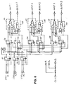
- another bus arbitrator 50A may be employed instead in order to avoid simultaneous contention or concurrent acknowledgment of the bus access signals I/OCS1 and I/OCS2 from the two controller units 10-1 and 10-2 .
- the bus arbitrator 50A is fed by two sampling clocks ⁇ 1 and ⁇ 2 of different phases such that I/OCS1 and I/OCS2 are acknowledged respectively at the rise time of the clocks ⁇ 1 and ⁇ 2 .
- I/OCS1 and I/OCS2 are latched respectively at flip-flops 51 and 52 .
- flip-flop 53 and 54 Another pair of flip-flops 53 and 54 is included to determine the priority between I/OCS1 and I/OCS2 in such a manner that flip-flop 53 latches the output of flip-flop 52 at a timing of flip-flop 51 latching I/OCS1 and that flip-flop 54 latches the output of flip-flop 51 at a timing of flip-flop 52 latching I/OCS2 . Also included are logic circuits 55 to 58 which produce the bus access signals BUSEN1 and BUSEN2 as well as the wait signals WAIT1 and WAIT2 .
- bus arbitrator 50A Operation of the bus arbitrator 50A is illustrated in the timing chart of FIG. 7. As seen from FIG. 7, the bus arbitrator 50A operates in the identical manner as the above mentioned arbitrator 50 except that I/OCS1 and I/OCS2 are acknowledged at different timings defined respectively by clocks ⁇ 1 and ⁇ 2 . Therefore, no duplicate explanation is deemed necessary.
- the present invention is not limited thereto and can be equally applicable to a three CPU system having three controller units each including the individual CPU for control of the associated I/O interface units independently from each other.
- the system includes a modified bus arbitrator 150 of FIG. 9 in which three sampling clocks ⁇ 1 , ⁇ 2 , and ⁇ 3 are utilized to acknowledge I/OCS1 , I/OCS2 , and I/OCS3 from the three controller units in order to avoid concurrent contention as seen in the bus arbitrator 50A of FIG. 6.
- the bus arbitrator 150 comprises flip-flops 151 to 159 for priority determination among I/OCS1 , I/OCS2 and I/OCS3 and also logic circuits 161 to 166 for producing the bus access signals BUSEN1 , BUSEN2 and BUSEN3 as well as the wait signals WAIT1 , WAIT2 , and WAIT3 .
- operations of the bus arbitrator 150 are of the same principle as the above mentioned bus arbitrator 50A . Therefore, no further explanation is deemed necessary.
- the I/O interface unit allocator 80 included in the system to correlate the individual I/O interface units 30-0 to 30-7 with the controller units 10-1 and 10-2 such that each I/O interface unit is set to be controlled exclusively by one of the controller units or commonly by the two controller units 10-1 and 10-2 .
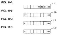
- the allocator 80 includes registers 81 to 84 of 8-bit structure.
- Register 81 is provided as a status register in order that the controller units 10-1 and 10-3 can identify by themselves as to the location on the base board 40 , i.e., which of the units is mounted into which of no. 1 and no. 2 slots in the base board 40 .
- a first bit D0 of register 81 is utilized to indicate that either of the controller units is mounted into no. 1 slot when "1" is entered and into no.2 slot when "0" is entered. That is, the system can identify the controller unit as the unit 10-1 when mounted in no.1 slot and as the unit 10-2 when mounted in no.2 slot.
- a fourth bit D3 is utilized to see whether additional controller unit is mounted or not. That is, "1" in bit D3 indicates the presence of the additional unit while "0" in bit D3 indicates the absence thereof. The remaining bits are left inoperative or no-op instruction.
- Register 82 is provided as an exclusive-use register with D0 to D7 bits corresponding to the I/O interface units 30-0 to 30-7 for setting the individual I/O interface units as being controlled exclusively by one of the controller units 10-1 and 10-2 . That is, when "1" is entered in the bit, the corresponding I/O interface unit is to be controlled exclusively by the controller unit 10-1 , while it is to be controlled exclusively by the other controller unit 10-2 when "0" is entered in the bit. It is noted that even if the controller unit should control any one of non-designated I/O interface unit, no data renewal is made for the output of that I/O interface unit as well as for the input to the controller unit therefrom.
- Register 83 is provided as a common-use register with DO to D7 bits corresponding to the I/O interface units 30-0 to 30-7 for setting the individual I/O interface units as being controlled commonly by the two controller units 10-1 and 10-2 .
- the corresponding I/O interface unit is set to be controlled commonly by the two controller units. This setting override the setting in the exclusive-use register 82 . Otherwise, or "0" is entered in a given bit, the corresponding I/O interface unit is set to be exclusively controlled in accordance with the setting in the exclusive-use register 82 .
- Register 84 is provided as a write register of which first bit D0 is linked to D3 bit of the status register 81 such that when "1" is entered in D0 bit of register 84 either of the controller units 10-1 or 10-2 checks whether the other controller unit is mounted on the base board 40 or not. Thus, "1" at D0 bit acts as additional CPU search flag for the above check.
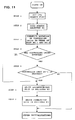
- FIG. 11 illustrates a flow chart for operation of thus configured I/O interface unit allocator 80 .
- the CPU search flag is set in the write register 84 such that the system can check whether the system includes one additional controller unit ⁇ step 1 ⁇ .
- content of the status register 81 is read [step 2], based upon which the allocator 80 identifies the location of the controller unit or units on the base board 40 in terms of the slot numbers [step 3].
- the allocator 80 checks whether the controller unit 10-1 in no. 1 slot is being processed [step 5]. If not, the routine proceeds to other initialization sequence of the system. If the controller unit 10-1 is acknowledged as being processed, the allocator 80 allows to write into the exclusive-use register 82 exclusive-use data indicating which of the I/O interface units 30-0 to 30-7 is or are exclusively controlled by which one of the controller units [step 6] followed by common-use data being written into the common-use register 83 indicating which of the I/O interface units 30-0 to 30-7 is or are commonly controlled by the two controller units 10-1 and 10-2 [step 7], after which the routine goes to the other initialization sequence.
- the controller unit 10-1 in no.1 slot is made responsible for writing the exclusive-use and common-use data into registers 82 and 83 . While, on the other hand, when only one of the controller units is recognized, the on-board controller unit is made responsible for writing the data into the registers.
- the controller units 10-1 and 10-2 are enabled to control independently from each other the associated I/O interface units.
- the common memory CM is a dual-port RAM of which ports are connected respectively to the internal memories M1 and M2 .
- One example of the data transfer is an data area dependent method in which each of the internal memories M1 and M2 is configured to have a particular exchange data area therein for storing data to be exchanged through the common memory CM . That is, as schematically shown in FIG.
- each of the internal memories M1 and M2 is configured to commonly store transfer-designation data A and B for the number of words and the beginning of address respectively written by the controller unit 10-1 ; and transfer-designation data C and D for the number of words and the beginning of address respectively written by the controller unit 10-2 , in addition to data to be transferred.
- the transfer-designation data A to D are transferred together with the actual data between M1 and M2 through CM under the control of the CPU of the controller units as an internal system processing separately from a user defined program.
- the common memory CM is configured to store, in addition to the actual data to be transferred, write flags F1 and F2 indicating as to whether the data have been transferred into the common memory CM from the internal memories M1 and M2 of the controller units 10-1 and 10-2 , respectively.
- F1 and F2 When “1" is assigned to F1 and F2 , it indicates that the data have been transferred into the common memory CM . Otherwise, or "0" in F1 and F2 indicates that data have not been transferred.
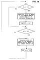
- the above data transfer is accomplished in accordance with the flow charts of FIGS. 15 and 16. FIG.
- FIG. 15 illustrates the data transfer between the internal memory M1 of the controller unit 10-1 and the common memory CM , in which data in area X1 in the internal memory M1 is transferred to area X2 in the common memory CM and data in area X5 of CM is transferred to area X6 of M1 , as schematically shown in FIG. 14.
- FIG. 16 illustrates the data transfer between the internal memory M2 of the controller unit 10-2 and the common memory CM , in which data in area X2 in the common memory CM is transferred to area X3 in the internal memory M2 and data in area X4 of M2 is transferred to area X5 of CM .
- the instruction comprises a write instruction and read instruction, schematically shown in FIGS. 17A and 17B, respectively.
- the write instruction of FIG. 17A is responsible for transferring data from the internal memory of one of the controller units to the internal memory of the other. That is, when the write instruction is programmed for the CPU of the controller unit 10-1 , data transfer is made from M1 to M2 , and when it is programmed for CPU of the controller unit 10-2 , data transfer is made from M2 to M1 .
- the write instruction comprises an operation code FN0 , a source address SRC indicating the beginning of the source address in the internal memory M1 or M2 , the number of words WRD of the data to be transferred from M1 or M2 , and a destination address DST indicating the beginning of the destination address in the internal memory M1 or M2 .
- the read instruction comprises, as shown in FIG.
- an operation code FN1 a source address SRC indicating the beginning of the source address in the internal memory M1 or M2 , the number of words WRD of the data to be transferred from M1 or M2 , and a destination address DST indicating the beginning of the destination address in the internal memory M1 or M2 .
- the write and read instructions are stored in the internal memories M1 and M2 , as schematically shown in FIG. 18A.
- the common memory CM is correspondingly configured to store write flags FW1 and FW2 indicating whether the data have been written or transferred together with the destination address DST to the common memory CM from the internal memory M1 and M2 , respectively; read flags FR1 and FR2 indicating as to whether there is requested to read and transfer the data from the common memory CM to the memories M1 and M2 , respectively; and the source address SRC , the number of words WRD , and destination address DST for each of M1 and M2 .
- FW1 and FW2 When “1" is given to FW1 and FW2 , it indicates that the data have been written or transferred to the common memory CM . Otherwise, or when "0" is given, FW1 and FW2 indicate that the data have not been written or transferred to CM . Likewise, FR1 and FR2 indicate that the data have been read from CM respectively to M1 and M2 when “1” is given, and not been read when "0" is given.
- FR1 or FR2 is given "1" in CM
- the CPU of the corresponding controller unit 10-2 or 10-1 which is requested to transfer the data into the common memory CM be read by the CPU of the other controller unit 10-1 or 10-2 , reads the source address SRC and the number of words WRD and transfers so specified data from its internal memory M2 or M1 to the common memory CM , after which the CPU resets FR1 or FR2 to "0".
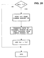
- FIGS. 19 and 20 illustrates the execution of the write instruction, for example, for transferring the data from the internal memory M1 of the controller unit 10-1 to the internal memory M2 of the other controller unit 10-2 through the common memory CM . That is, the write instruction is executed in accordance with the flow chart of FIG. 19 comprising the steps in which the CPU of the controller unit 10-1 transfers the data corresponding to the specified source address S1 and the number of words WRD from the internal memory M1 to the common memory CM , and write the destination address DST into the common memory followed by resetting FW1 to "1". Then, the sequence proceeds in accordance with the flow chart of FIG.
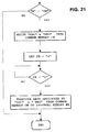
- FIGS. 21 and 22 illustrates the execution of read instruction, for example, for reading the data from the internal memory M2 to the internal memory M1 through the common memory CM .
- the read instruction is executed firstly in accordance with the flow chart of FIG.
- FIGS. 19 to 22 illustrate the write and read instructions from the CPU of the controller unit 10-1 , these instructions from the CPU of the other controller unit 10-2 can be executed in the like manner.
Landscapes
- Engineering & Computer Science (AREA)
- Theoretical Computer Science (AREA)
- Physics & Mathematics (AREA)
- General Engineering & Computer Science (AREA)
- General Physics & Mathematics (AREA)
- Computer Hardware Design (AREA)
- Software Systems (AREA)
- Programmable Controllers (AREA)
- Bus Control (AREA)
Applications Claiming Priority (6)
| Application Number | Priority Date | Filing Date | Title |
|---|---|---|---|
| JP172896/91 | 1991-07-15 | ||
| JP3172896A JPH04363751A (ja) | 1991-02-25 | 1991-07-15 | マルチcpuシステム |
| JP3340450A JPH05173986A (ja) | 1991-12-24 | 1991-12-24 | プログラマブルコントローラ |
| JP340450/91 | 1991-12-24 | ||
| JP12514/92 | 1992-01-28 | ||
| JP01251492A JP3314948B2 (ja) | 1992-01-28 | 1992-01-28 | マルチcpu構成のプログラマブルコントローラにおけるデータ交換方式 |
Publications (2)
| Publication Number | Publication Date |
|---|---|
| EP0523627A2 true EP0523627A2 (fr) | 1993-01-20 |
| EP0523627A3 EP0523627A3 (en) | 1993-08-25 |
Family
ID=27279860
Family Applications (1)
| Application Number | Title | Priority Date | Filing Date |
|---|---|---|---|
| EP19920111983 Withdrawn EP0523627A3 (en) | 1991-07-15 | 1992-07-14 | Multi-cpu programmable controller |
Country Status (3)
| Country | Link |
|---|---|
| US (1) | US5432911A (fr) |
| EP (1) | EP0523627A3 (fr) |
| KR (1) | KR970001902B1 (fr) |
Cited By (1)
| Publication number | Priority date | Publication date | Assignee | Title |
|---|---|---|---|---|
| US6434638B1 (en) | 1994-12-09 | 2002-08-13 | International Business Machines Corporation | Arbitration protocol for peer-to-peer communication in synchronous systems |
Families Citing this family (12)
| Publication number | Priority date | Publication date | Assignee | Title |
|---|---|---|---|---|
| WO1994010632A1 (fr) * | 1992-11-04 | 1994-05-11 | Siemens Aktiengesellschaft | Agencement regroupant plusieurs utilisateurs actifs et passifs de bus |
| US5669009A (en) * | 1994-06-30 | 1997-09-16 | Hughes Electronics | Signal processing array |
| KR0155269B1 (ko) * | 1995-01-16 | 1998-11-16 | 김광호 | 버스 중재방법 및 그 장치 |
| US5687091A (en) * | 1995-06-08 | 1997-11-11 | Automatic Control Technologies | Integrated arrangement for monitoring without interrupt process flow by novel sensor arrangement with unique data processing system |
| US5874931A (en) * | 1996-06-28 | 1999-02-23 | Microchip Technology Incorporated | Microcontroller with dual port ram for LCD display and sharing of slave ports |
| EP0960372A2 (fr) * | 1997-10-29 | 1999-12-01 | Koninklijke Philips Electronics N.V. | Procede et systeme pour synchroniser le transfert de donnees organisees en blocs |
| US6523076B1 (en) * | 1999-11-08 | 2003-02-18 | International Business Machines Corporation | Method and apparatus for synchronizing multiple bus arbiters on separate chips to give simultaneous grants for the purpose of breaking livelocks |
| JP2006501361A (ja) * | 2002-05-08 | 2006-01-12 | エイケイ・プロパティーズ・インコーポレイテッド | 無方向性電磁鋼ストリップの連続鋳造方法 |
| KR20050023699A (ko) * | 2003-09-02 | 2005-03-10 | 삼성전자주식회사 | 복수의 cpu 시스템에서 디바이스를 공유하는 방법 및장치 |
| TWI277877B (en) * | 2005-03-08 | 2007-04-01 | Via Tech Inc | Method and related apparatus for monitoring system bus |
| US8706262B2 (en) | 2011-03-15 | 2014-04-22 | Omron Corporation | CPU unit of PLC, system program for PLC, and recording medium storing system program for PLC |
| US9563590B2 (en) * | 2014-03-17 | 2017-02-07 | Nxp Usa, Inc. | Devices with arbitrated interface busses, and methods of their operation |
Family Cites Families (9)
| Publication number | Priority date | Publication date | Assignee | Title |
|---|---|---|---|---|
| US3959775A (en) * | 1974-08-05 | 1976-05-25 | Gte Automatic Electric Laboratories Incorporated | Multiprocessing system implemented with microprocessors |
| US4442504A (en) * | 1981-03-09 | 1984-04-10 | Allen-Bradley Company | Modular programmable controller |
| US4549273A (en) * | 1982-12-10 | 1985-10-22 | Ael Microtel Limited | Memory access control circuit |
| DE3751609T2 (de) * | 1986-09-01 | 1996-07-04 | Nippon Electric Co | Datenprozessor mit Hochgeschwindigkeitsdatenübertragung. |
| US4858101A (en) * | 1987-08-26 | 1989-08-15 | Allen-Bradley Company, Inc. | Programmable controller with parallel processors |
| US4937777A (en) * | 1987-10-07 | 1990-06-26 | Allen-Bradley Company, Inc. | Programmable controller with multiple task processors |
| US5003463A (en) * | 1988-06-30 | 1991-03-26 | Wang Laboratories, Inc. | Interface controller with first and second buffer storage area for receiving and transmitting data between I/O bus and high speed system bus |
| IT1229667B (it) * | 1989-04-24 | 1991-09-06 | Bull Hn Information Syst | Sistema di elaborazione dati con arbitratore duale di accesso a bus di sistema. |
| US5301330A (en) * | 1990-10-12 | 1994-04-05 | Advanced Micro Devices, Inc. | Contention handling apparatus for generating user busy signal by logically summing wait output of next higher priority user and access requests of higher priority users |
-
1992
- 1992-07-14 EP EP19920111983 patent/EP0523627A3/en not_active Withdrawn
- 1992-07-14 US US07/913,690 patent/US5432911A/en not_active Expired - Lifetime
- 1992-07-15 KR KR1019920012562A patent/KR970001902B1/ko not_active Expired - Fee Related
Cited By (1)
| Publication number | Priority date | Publication date | Assignee | Title |
|---|---|---|---|---|
| US6434638B1 (en) | 1994-12-09 | 2002-08-13 | International Business Machines Corporation | Arbitration protocol for peer-to-peer communication in synchronous systems |
Also Published As
| Publication number | Publication date |
|---|---|
| KR970001902B1 (ko) | 1997-02-18 |
| US5432911A (en) | 1995-07-11 |
| KR930002962A (ko) | 1993-02-23 |
| EP0523627A3 (en) | 1993-08-25 |
Similar Documents
| Publication | Publication Date | Title |
|---|---|---|
| US6014729A (en) | Shared memory arbitration apparatus and method | |
| US6247100B1 (en) | Method and system for transmitting address commands in a multiprocessor system | |
| DE3788805T2 (de) | Prioritaetstechnik für einen zerteilten transaktionsbus in einem multiprozessorrechnersystem. | |
| EP0318221B1 (fr) | Commande des réponses d'utilisateurs dans un bus d'intercommunication | |
| EP0450233B1 (fr) | Accès de bus pour système calculateur numérique | |
| EP0523627A2 (fr) | Unité de commande programmable pour plusieurs unités centrales de traitement | |
| US4797815A (en) | Interleaved synchronous bus access protocol for a shared memory multi-processor system | |
| EP0428330A2 (fr) | Circuit interface de calculateur | |
| US4417303A (en) | Multi-processor data communication bus structure | |
| HUT57923A (en) | Hold and lock circuit regulating bus service for microprocessor systems | |
| KR100708096B1 (ko) | 버스 시스템 및 그 실행 순서 조정방법 | |
| US5455912A (en) | High speed/low overhead bus arbitration apparatus and method for arbitrating a system bus | |
| EP0479229B1 (fr) | Système multiprocesseur à double bus avec contention de bus minimale | |
| US5828852A (en) | Method for operation of a bus system for highly flexible and quick data transmission between units connected to the bus system and configuration for carrying out the method | |
| JPS59218532A (ja) | バス接続方式 | |
| JPH05282242A (ja) | バス制御方式 | |
| JP3314948B2 (ja) | マルチcpu構成のプログラマブルコントローラにおけるデータ交換方式 | |
| KR930004910Y1 (ko) | 다중처리기 시스템에서의 데이터버스 중재기 | |
| JP2705955B2 (ja) | 並列情報処理装置 | |
| JPS6341970A (ja) | マイクロコンピユ−タシステム | |
| JPS62197851A (ja) | バス制御装置 | |
| JPS5975354A (ja) | プロセッサ装置 | |
| JPS63133257A (ja) | マルチプロセサ方式 | |
| JPH0310354A (ja) | データ転送制御システム | |
| CN1012295B (zh) | 中央处理器代表无判优功能外设进行判优的存储器直接存取访问判优设备 |
Legal Events
| Date | Code | Title | Description |
|---|---|---|---|
| PUAI | Public reference made under article 153(3) epc to a published international application that has entered the european phase |
Free format text: ORIGINAL CODE: 0009012 |
|
| 17P | Request for examination filed |
Effective date: 19920714 |
|
| AK | Designated contracting states |
Kind code of ref document: A2 Designated state(s): DE GB |
|
| PUAL | Search report despatched |
Free format text: ORIGINAL CODE: 0009013 |
|
| AK | Designated contracting states |
Kind code of ref document: A3 Designated state(s): DE GB |
|
| 17Q | First examination report despatched |
Effective date: 19960722 |
|
| STAA | Information on the status of an ep patent application or granted ep patent |
Free format text: STATUS: THE APPLICATION IS DEEMED TO BE WITHDRAWN |
|
| 18D | Application deemed to be withdrawn |
Effective date: 19961203 |