EP0523716B1 - Infrarotsensor und sein Herstellungsverfahren - Google Patents
Infrarotsensor und sein Herstellungsverfahren Download PDFInfo
- Publication number
- EP0523716B1 EP0523716B1 EP92112228A EP92112228A EP0523716B1 EP 0523716 B1 EP0523716 B1 EP 0523716B1 EP 92112228 A EP92112228 A EP 92112228A EP 92112228 A EP92112228 A EP 92112228A EP 0523716 B1 EP0523716 B1 EP 0523716B1
- Authority
- EP
- European Patent Office
- Prior art keywords
- infrared
- silicon
- films
- infrared sensor
- silicon compound
- Prior art date
- Legal status (The legal status is an assumption and is not a legal conclusion. Google has not performed a legal analysis and makes no representation as to the accuracy of the status listed.)
- Expired - Lifetime
Links
- 238000004519 manufacturing process Methods 0.000 title claims description 12
- XUIMIQQOPSSXEZ-UHFFFAOYSA-N Silicon Chemical compound [Si] XUIMIQQOPSSXEZ-UHFFFAOYSA-N 0.000 claims description 52
- 229910052710 silicon Inorganic materials 0.000 claims description 52
- 239000010703 silicon Substances 0.000 claims description 52
- 239000000758 substrate Substances 0.000 claims description 52
- 238000000034 method Methods 0.000 claims description 36
- 229910021331 inorganic silicon compound Inorganic materials 0.000 claims description 27
- 239000004065 semiconductor Substances 0.000 claims description 15
- GNPVGFCGXDBREM-UHFFFAOYSA-N germanium atom Chemical compound [Ge] GNPVGFCGXDBREM-UHFFFAOYSA-N 0.000 claims description 12
- 229910052732 germanium Inorganic materials 0.000 claims description 11
- VYPSYNLAJGMNEJ-UHFFFAOYSA-N Silicium dioxide Chemical compound O=[Si]=O VYPSYNLAJGMNEJ-UHFFFAOYSA-N 0.000 claims description 7
- 239000007789 gas Substances 0.000 claims description 7
- 238000000059 patterning Methods 0.000 claims description 7
- 229910052814 silicon oxide Inorganic materials 0.000 claims description 7
- 229910052581 Si3N4 Inorganic materials 0.000 claims description 5
- 229910021417 amorphous silicon Inorganic materials 0.000 claims description 5
- HQVNEWCFYHHQES-UHFFFAOYSA-N silicon nitride Chemical compound N12[Si]34N5[Si]62N3[Si]51N64 HQVNEWCFYHHQES-UHFFFAOYSA-N 0.000 claims description 5
- 229910021420 polycrystalline silicon Inorganic materials 0.000 claims description 4
- OKTJSMMVPCPJKN-UHFFFAOYSA-N Carbon Chemical compound [C] OKTJSMMVPCPJKN-UHFFFAOYSA-N 0.000 claims description 3
- 229910052799 carbon Inorganic materials 0.000 claims description 3
- 230000005855 radiation Effects 0.000 description 22
- GQPLMRYTRLFLPF-UHFFFAOYSA-N Nitrous Oxide Chemical compound [O-][N+]#N GQPLMRYTRLFLPF-UHFFFAOYSA-N 0.000 description 12
- 230000015572 biosynthetic process Effects 0.000 description 8
- 238000005530 etching Methods 0.000 description 8
- 239000010410 layer Substances 0.000 description 8
- PXHVJJICTQNCMI-UHFFFAOYSA-N nickel Substances [Ni] PXHVJJICTQNCMI-UHFFFAOYSA-N 0.000 description 7
- 238000004544 sputter deposition Methods 0.000 description 7
- XKRFYHLGVUSROY-UHFFFAOYSA-N Argon Chemical compound [Ar] XKRFYHLGVUSROY-UHFFFAOYSA-N 0.000 description 4
- OAKJQQAXSVQMHS-UHFFFAOYSA-N Hydrazine Chemical compound NN OAKJQQAXSVQMHS-UHFFFAOYSA-N 0.000 description 4
- KWYUFKZDYYNOTN-UHFFFAOYSA-M Potassium hydroxide Chemical compound [OH-].[K+] KWYUFKZDYYNOTN-UHFFFAOYSA-M 0.000 description 4
- BLRPTPMANUNPDV-UHFFFAOYSA-N Silane Chemical compound [SiH4] BLRPTPMANUNPDV-UHFFFAOYSA-N 0.000 description 4
- -1 for example Substances 0.000 description 4
- PCHJSUWPFVWCPO-UHFFFAOYSA-N gold Chemical compound [Au] PCHJSUWPFVWCPO-UHFFFAOYSA-N 0.000 description 4
- 239000010931 gold Substances 0.000 description 4
- 229910052737 gold Inorganic materials 0.000 description 4
- 238000001020 plasma etching Methods 0.000 description 4
- IJGRMHOSHXDMSA-UHFFFAOYSA-N Atomic nitrogen Chemical compound N#N IJGRMHOSHXDMSA-UHFFFAOYSA-N 0.000 description 3
- 229910017817 a-Ge Inorganic materials 0.000 description 3
- XAGFODPZIPBFFR-UHFFFAOYSA-N aluminium Chemical compound [Al] XAGFODPZIPBFFR-UHFFFAOYSA-N 0.000 description 3
- 229910052782 aluminium Inorganic materials 0.000 description 3
- 239000013078 crystal Substances 0.000 description 3
- 239000000203 mixture Substances 0.000 description 3
- 229910052759 nickel Inorganic materials 0.000 description 3
- 238000005268 plasma chemical vapour deposition Methods 0.000 description 3
- 230000035945 sensitivity Effects 0.000 description 3
- 238000010521 absorption reaction Methods 0.000 description 2
- 229910052786 argon Inorganic materials 0.000 description 2
- 238000010276 construction Methods 0.000 description 2
- 238000001514 detection method Methods 0.000 description 2
- 230000000694 effects Effects 0.000 description 2
- 235000013842 nitrous oxide Nutrition 0.000 description 2
- 238000012545 processing Methods 0.000 description 2
- 230000001846 repelling effect Effects 0.000 description 2
- 238000001947 vapour-phase growth Methods 0.000 description 2
- XPDWGBQVDMORPB-UHFFFAOYSA-N Fluoroform Chemical compound FC(F)F XPDWGBQVDMORPB-UHFFFAOYSA-N 0.000 description 1
- 229910004304 SiNy Inorganic materials 0.000 description 1
- 238000004458 analytical method Methods 0.000 description 1
- 238000000137 annealing Methods 0.000 description 1
- 239000007864 aqueous solution Substances 0.000 description 1
- QVGXLLKOCUKJST-UHFFFAOYSA-N atomic oxygen Chemical compound [O] QVGXLLKOCUKJST-UHFFFAOYSA-N 0.000 description 1
- 230000036760 body temperature Effects 0.000 description 1
- 238000005229 chemical vapour deposition Methods 0.000 description 1
- 239000011248 coating agent Substances 0.000 description 1
- 238000000576 coating method Methods 0.000 description 1
- 238000012937 correction Methods 0.000 description 1
- 230000007812 deficiency Effects 0.000 description 1
- 238000000151 deposition Methods 0.000 description 1
- 230000002708 enhancing effect Effects 0.000 description 1
- 238000001659 ion-beam spectroscopy Methods 0.000 description 1
- 238000010884 ion-beam technique Methods 0.000 description 1
- 238000004518 low pressure chemical vapour deposition Methods 0.000 description 1
- 239000000463 material Substances 0.000 description 1
- 238000005259 measurement Methods 0.000 description 1
- UNRFQJSWBQGLDR-UHFFFAOYSA-N methane trihydrofluoride Chemical compound C.F.F.F UNRFQJSWBQGLDR-UHFFFAOYSA-N 0.000 description 1
- 229910001120 nichrome Inorganic materials 0.000 description 1
- 239000001301 oxygen Substances 0.000 description 1
- 229910052760 oxygen Inorganic materials 0.000 description 1
- 230000002093 peripheral effect Effects 0.000 description 1
- 238000007747 plating Methods 0.000 description 1
- 229920001296 polysiloxane Polymers 0.000 description 1
- 238000005001 rutherford backscattering spectroscopy Methods 0.000 description 1
- 239000002356 single layer Substances 0.000 description 1
- 239000000243 solution Substances 0.000 description 1
- 239000000126 substance Substances 0.000 description 1
- 238000012360 testing method Methods 0.000 description 1
- 210000003454 tympanic membrane Anatomy 0.000 description 1
- 238000001771 vacuum deposition Methods 0.000 description 1
Images

Classifications
-
- H—ELECTRICITY
- H10—SEMICONDUCTOR DEVICES; ELECTRIC SOLID-STATE DEVICES NOT OTHERWISE PROVIDED FOR
- H10F—INORGANIC SEMICONDUCTOR DEVICES SENSITIVE TO INFRARED RADIATION, LIGHT, ELECTROMAGNETIC RADIATION OF SHORTER WAVELENGTH OR CORPUSCULAR RADIATION
- H10F30/00—Individual radiation-sensitive semiconductor devices in which radiation controls the flow of current through the devices, e.g. photodetectors
- H10F30/10—Individual radiation-sensitive semiconductor devices in which radiation controls the flow of current through the devices, e.g. photodetectors the devices being sensitive to infrared radiation, visible or ultraviolet radiation, and having no potential barriers, e.g. photoresistors
- H10F30/15—Individual radiation-sensitive semiconductor devices in which radiation controls the flow of current through the devices, e.g. photodetectors the devices being sensitive to infrared radiation, visible or ultraviolet radiation, and having no potential barriers, e.g. photoresistors comprising amorphous semiconductors
-
- G—PHYSICS
- G01—MEASURING; TESTING
- G01J—MEASUREMENT OF INTENSITY, VELOCITY, SPECTRAL CONTENT, POLARISATION, PHASE OR PULSE CHARACTERISTICS OF INFRARED, VISIBLE OR ULTRAVIOLET LIGHT; COLORIMETRY; RADIATION PYROMETRY
- G01J5/00—Radiation pyrometry, e.g. infrared or optical thermometry
- G01J5/10—Radiation pyrometry, e.g. infrared or optical thermometry using electric radiation detectors
- G01J5/20—Radiation pyrometry, e.g. infrared or optical thermometry using electric radiation detectors using resistors, thermistors or semiconductors sensitive to radiation, e.g. photoconductive devices
Definitions
- This invention relates to an infrared sensor for noncontact measurement of the temperature of an object under test such as tympanic membrane, and a method for the production thereof.
- the infrared sensor has a construction completed by forming a micro bridge portion formed on a sensor substrate and further forming an infrared sensing portion on the bridge portion.
- the bridge structure which has the thermosensitive portion of device suspended after the fashion of a bridge above the supporting substrate is intended to improve the sensitivity of response of the device.
- the infrared sensing portions which are used in the infrared sensors may be classified into those of the bolometer type having the resistance of a device varied proportionately to a change caused in the sensor temperature by infrared radiation, those of the thermopile type having the electromotive force of a device varied similarly, and those of the pyroelectric type having the electromotive force of a device varied proportionately to a change in the dose of infrared radiation.
- the infrared sensing portions of the bolometer type allow miniaturization of their sensors as because they are capable of directly indicating temperature from the magnitude of resistance.
- the infrared sensor of the bolometer type is generally provided with at least two infrared sensing portions, one of which is adapted to admit infrared radiation and the other shielded from infrared radiation.
- this sensor is enabled to detect accurately the net dose of infrared radiation free from electrical noise and thermal disturbance.
- the conventional infrared sensor has these at least two infrared sensing portions formed on only one of the opposite surfaces of a semiconductor wafer or substrate which serves as the sensor substrate.
- the conventional infrared sensor Since the conventional infrared sensor has at least two infrared sensing portions formed only on one of the opposite surfaces of the sensor substrate, it is difficult to allow the infrared radiation to impinge solely on one of the infrared sensing portions and prevent it from impinging on the other infrared sensing portion. From the differential outputs of these two infrared sensing portions, therefore, the net dose of impinging infrared radiation cannot be accurately detected. The data of determination consequently obtained must be subjected to various corrections. Further, the conventional infrared sensor has a limit to the overall miniaturization thereof because of the fact that two or more infrared sensing portions are formed on one and the same surface of the sensor substrate, coupled with the problem of shielding against the infrared radiation.
- An object of this invention is to provide a novel infrared sensor and a method for the production thereof.
- Another object of this invention is to provide an infrared sensor which allows generous overall miniaturisation thereof, enables the infrared radiation to impinge infallibly on a specific infrared sensing portion exclusively, and warrants accurate detection of the dose of infrared radiation and a method for the production of the infrared sensor.
- the infrared sensor of this invention allows generous miniaturization of itself specifically to one half the size of the conventional countertype and enables the differential output between the two infrared sensing portions on the opposite surfaces thereof to be detected accurately and enjoys an effect in improving the accuracy of determination because it is so constructed as to have infrared sensing films formed one each on the opposite surfaces of a semiconductor substrate. It is, therefore, used advantageously as a veritably miniature sensor such as, for example, a thermometer adapted to measure the body temperature of a user by having a sensor portion thereof inserted in the ear.
- the bridge portions on the opposite surfaces of the semiconductor substrate are improved in stress balance and stabilized in structure because they are formed of a film of an inorganic silicon compound, particularly a film of silicon oxynitride.
- the infrared sensor of this invention is enabled to acquire ample strength and ideal sensitivity because the film of an inorganic silicon compound, particularly silicon oxynitride, is given a wall thickness in the range between about 0.1 and about 50 ⁇ m.
- the method of this invention for the production of an infrared sensor produces an effect of notably improving the yield of products because the bridge portions are formed of a film of an inorganic silicon compound, particularly silicon oxynitride.
- the infrared sensor of this invention has infrared sensing portions formed one each on the opposite surfaces of a sensor substrate. Owing to this construction, the total surface area of the sensor may be one half that of the conventional sensor in spite of the equal number of infrared sensing portions and the sensor is allowed a generous reduction in size. Further, since the infrared sensing portions are distributed between the opposite surfaces of the sensor substrate, the sensor substrate which intervenes between the infrared sensing portions fulfills the role of an infrared intercepting member and renders it easy to limit the selective impingement of infrared radiation only to the infrared sensing portion on one of the opposite surfaces.
- the infrared sensing films are improved in efficiency of absorption and in accuracy of infrared detection.
- the infrared absorbing films are made of gold black or carbon, for example, and are desired to have a thickness in the range between about 0.3 and about 10 ⁇ m, preferably between 0.3 and 2 ⁇ m.
- a semiconductor substrate made of silicon or germanium may be used.
- a silicon substrate which can be procured easily and inexpensively is used.
- the infrared sensing portions are formed of a film of amorphous germanium (a-Ge), amorphous silicon (a-Si), or polycrystalline silicon, for example.
- a-Ge amorphous germanium
- a-Si amorphous silicon
- polycrystalline silicon for example.
- sputtering, ion beam spattering, or CVD (chemical vapor-phase growth) method may be used, for example.
- the infrared sensor of this invention is preferable to be produced by a procedure which comprises forming bridge portions (bridges) one each on the opposite surfaces of the sensor substrate and superposing the infrared sensing portions one each on the bridge portions.
- the bridge portions may be formed of a film of an inorganic silicon compound such as, for example, silicon oxide (SiO x ) film, silicon nitride (SiN y ) film, or silicone oxynitride (SiO x N y ) film, for example.
- they are formed of a silicon oxynitride film.
- the silicon oxynitride film combines the qualities of both the silicon oxide film and silicon nitride film.
- the optimum conditions for the formation of the silicon oxynitride film vary with the particular kind of the sensor substrate to be used because the thermal expansion coefficient of the film varies with the orientation of the crystal surface of the material for the substrate.
- the thickness of the silicon oxynitride film is preferable to be in the range between 0.1 and 50 ⁇ m, preferably between about 0.5 and about 5 ⁇ m. If the thickness is less than 0.1 ⁇ m, the film is too thin to acquire ample strength. Conversely, if the thickness exceeds 50 ⁇ m, the film acquires a large thermal capacity and consequently suffers from deficiency in sensitivity.
- the method of this invention for the production of a bolometer type infrared sensor comprises a step of advancing a reactive gas into contact with a semiconductor substrate thereby forming inorganic silicon compound films one each on the opposite surfaces of the semiconductor substrate, a step of subjecting the inorganic silicon compound films formed on the opposite surfaces of the semiconductor substrate to a patterning treatment, a step of superposing infrared sensing portions one each on the patterned inorganic silicon compound films, and a step of selectively removing the semiconductor substrates underlying the patterned inorganic silicon compound films thereby forming cavities beneath the films and consequently forming bridge portions of inorganic silicon compound film one each on the opposite surfaces of the semiconductor substrate.
- the formation of the inorganic silicon compound films is specifically carried out by the plasma CVD method, for example.
- monosilane (SiH 4 ), nitrogen (N 2 ), and laughing gas (N 2 O) are used as reactive gases.
- N 2 /(N 2 + N 2 O) the stoichiometric compositions x and y of the silicon oxynitride film (SiO x N y ) can be controlled, the difference in thermal expansion coefficient between the film and the silicon substrate can be substantially eliminated, and the possible damage by stress can be precluded.
- the method employed for the formation of the silicon oxynitride film needs not be limited to the plasma CVD method. Some other method such as, for example, sputtering method may be used instead. By this sputtering low pressure CVD method and method, it suffices to form the silicon oxynitride film by using silicon oxide as a target. In this case, the composition of the silicon oxynitride film can be varied by incorporating nitrogen (N 2 ) into the sputtering gas such as, for example, argon (Ar).
- the patterning on the inorganic silicon compound films is carried out by the reactive ion etching method, for example.
- the superposition of the infrared sensing portions on the patterned inorganic silicon compound films is carried out by the sputtering method, ion beam sputtering method, or CVD method using amorphous germanium, amorphous silicon, or polycrystalline silicon, for example.
- the formation of the bridge portions is effected by selectively removing by etching the sensor substrate underlying the patterned inorganic silicon compound films with an aqueous solution of hydrazine, potassium hydroxide, etc., for example, thereby forming cavities beneath the films.
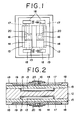
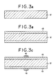
- Fig. 1 represents a plan structure of an infrared sensor as one embodiment of this invention and Fig. 2 is a cross section taken through Fig. 1 along the line II-II.
- cavities 13 are formed one each on the opposite surfaces of a silicon substrate 12 as the sensor substrate. Further, on the opposite surfaces of the silicon substrate 12, inorganic silicon compound films such as, for example, silicon oxynitride films 15 severally provided with bridge portions 14 measuring 100 ⁇ m in width, 2 mm in length, and 2 ⁇ m in thickness are formed one each on the cavities 13. Infrared sensing portions 16 are formed in the upper central portions of the bridge portions 14. These infrared sensing portions 16 are formed of amorphous germanium (a-Ge), for example. To the infrared sensing portions 16 are electrically connected one-terminal portions of electrode connecting layers 17. The connecting layers 17 are formed of an aluminum (Al) film.
- Al aluminum
- connecting layers 17 are integrated with electrode pads 18 which are formed in the peripheral portion of the silicon substrate 12.
- inorganic silicon compound films such as, for example, silicon oxynitride films 19 are superposed as insulating films.
- silicon oxynitride films 19 are superposed as insulating films.
- infrared absorbing films 20 having a thickness of about 0.5 ⁇ m are formed so as to cover the infrared sensing portions 16.
- These infrared absorbing films 20 are intended to heighten the infrared sensing portions 16 in efficiency of absorption of infrared radiation. They are formed of gold black or nichrome, for example.
- the intercepting member 21 such as Ni is formed on the cavity 13 so that the infrared from the surface of the substrate is sufficiently intercepted.
- the magnitude of electric resistance of the infrared sensing portions 16 is varied proportionately to the amount of impinging infrared radiation (heat quantity).
- the amount of infrared radiation can be detected by measuring the magnitude of electric current flowing through the electrode connecting layers 17 proportionately to the change in the magnitude of resistance or the magnitude of voltage between the electrode pads 18 by means of a signal processing circuit (not shown).
- infrared radiation can be sufficienly intercepted by an infrared-intercepting member 21 made of, e.g., nickel and renders it easy to limit selective impingement of infrared radiation to the infrared sensing portion 16 on one of the opposite surfaces.
- an infrared-intercepting member 21 made of, e.g., nickel and renders it easy to limit selective impingement of infrared radiation to the infrared sensing portion 16 on one of the opposite surfaces.
- the infrared radiation is allowed to impinge only on the two infrared sensing films 16 on the upper surface, the infrared radiation is not impinged in to the two infrared sensing portions 16 on the reverse surface of the silicon substrate 12, because it is sufficiently intercepted by the intercepting member 21 made of, e,g., nickel.
- the differential output between the infrared sensing portion 16 admitting the impingement of infrared radiation and the infrared sensing portion 16 repelling the infrared radiation can be accurately obtained.
- the infrared sensor 11 performs the determination with enhanced accuracy.
- the total surface area of the sensor may be one half that of the conventional sensor in spite of the equal number of infrared sensing portions 16 and the infrared sensor allows a generous reduction in size.
- the bridge portions 14 on the opposite surfaces are formed of a single-layer silicon oxynitride film 15 excelling in stress balance, the possible difference in thermal expansion coefficient between the film and the silicon substrate 12 can be substantially eliminated. As a result, the bridge structures are so stable that the possibility of the structures sustaining damage during the process of production is nil.
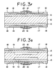
- Figs. 3A to 3G jointly represent a process of production of the infrared sensor.
- a silicon substrate 12 having a crystal face orientation (110) as illustrated in Fig. 3A was prepared.
- silicon oxynitride films (SiO x N y ) 15 were formed one each in a thickness of 2 ⁇ m on the opposite surfaces of the silicon substrate 12 by the plasma CVD method as illustrated in Fig. 3B.
- the silicon substrate 12 was kept heated at 450°C and, under the film-forming conditions of 0.60 hPa (0.45 Torr) of pressure and 400 W of high-frequency output, the hot silicon substrate 12 was swept with reactive gases, i.e.
- RIE reactive ion etching
- methane trifluoride (CHF 3 ) and oxygen (O 2 ) were fed as etching gases at respective flow volumes of 47.5 SCCM and 2.5 SCCM under a pressure 10.0 Pa (0.075 Torr) at a high-frequency output of 150 W for three hours.
- infrared sensing portions 16 were formed one each in the central portions of the bridge portions 14 on the opposite surfaces as illustrated in Fig. 3C.
- amorphous germanium (a-Ge) films were superposed on the silicon oxynitride films 15 and silicon substrate 12 by subjecting the films 15 and substrate 12 to a sputtering treatment using germanium (Ge) as a target.
- This sputtering was carried out by feeding argon (Ar) at flow volumes of 4 SCCM under a pressure of 67 Pa (5 x 10 -3 Torr) at a high-frequency pressure of 200 W for 10 minutes.
- the superposed amorphous germanium films were subjected to an annealing treatment at 500°C to accelerate polycrystallization of the amorphous germanium.
- the resultant polycrystallized amorphous germanium films were patterned by a reactive ion etching treatment.
- insulating films such as, for example, silicon oxynitride films 19, were formed one each in a thickness of 1 ⁇ m on the opposite surfaces of the silicon substrate 12 except for the regions of the electrode pad portions 18 as illustrated in Fig. 3E.
- the formation of these films was performed under the same conditions as those used in the step of Fig. 3B for 10 minutes.
- infrared absorbing films 20 were formed one each in a thickness of 0.5 ⁇ m on the silicon oxynitride films 19 by the liftoff method as illustrated in Fig. 3F.
- the infrared absorbing films 20 were selectively formed by coating the silicon oxynitride films 19 each with a positive resist film, patterning the positive resist films, vacuum depositing gold black thereon under a pressure of 27 Pa (0.2 Torr), and thereafter removing the positive resist films in conjunction with unnecessary portion of gold black.
- the silicon substrate 12 underlying the bridge portions on the opposite surfaces was selectively removed by etching to form cavities 13 as illustrated in Fig. 3G.
- This removal was effected by the anisotropic etching method using an aqueous hydrazine solution.
- an aqueous potassium hydroxide solution may be used for this anisotropic etching method.
- surface of silicon substrate is selectively plated with nickel film in thickness of 0.5 ⁇ m at the cavities 13 by monelectrolytic plating to form infrared-intercepting film 21 and an infrared sensor having a cross section as shown in Fig. 2.
- the bridge portions 14 were formed in a linear shape and constructed to be supported at two points. Optionally, they may be constructed to be supported at three points for the purpose of further enhancing strength. While the bridge portions 14 were formed in a flat shape along the surface of the silicon substrate 12 in the working example, they may be formed in an arcuate shape. While the bridge portions 14 were formed each with a silicon oxynitride film in the working example, they may be formed with a silicon oxide film or silicon nitride film. Further in the working example, the bridge portions 14 were formed by the excavating method resorting to the anisotropic etching technique. Optionally, they may be formed by some other method such as, for example, the socalled sacrifice layer method which requires the bridge portions 14 to be underlain preparatorily by an etching layer.
Landscapes
- Physics & Mathematics (AREA)
- General Physics & Mathematics (AREA)
- Spectroscopy & Molecular Physics (AREA)
- Photometry And Measurement Of Optical Pulse Characteristics (AREA)
- Radiation Pyrometers (AREA)
Claims (15)
- Infrarotsensor, umfassend ein Sensorsubstrat (12), das gegenüberliegende Oberflächen aufweist und aus einem Halbleitermaterial gebildet ist, Vertiefungen (13), die auf den gegenüberliegenden Oberflächen des Sensorsubstrats gebildet sind, Brückenabschnitte (14), die auf jeder Vertiefung gebildet sind, und einen Satz von Infrarotabtastabschnitten (16), die auf jedem der Brückenabschnitte gebildet sind.
- Infrarotsensor nach Anspruch 1, bei dem die Brückenabschnitte jeweils aus einem Film (19) aus einer anorganischen Siliciumverbindung gebildet sind.
- Infrarotsensor nach Anspruch 2, bei dem die anorganische Siliciumverbindung ausgewählt ist aus der Gruppe bestehend aus Siliciumoxid, Siliciumnitrid und Siliciumoxynitrid.
- Infrarotsensor nach Anspruch 2, bei dem die anorganische Siliciumverbindung Siliciumoxynitrid ist.
- Infrarotsensor nach einem der Ansprüche 3 bis 4, bei dem die Dicke des Films der anorganischen Siliciumverbindung im Bereich zwischen 0,1 und 50 µm ist.
- Infrarotsensor nach Anspruch 5, bei dem die Dicke des Films der anorganischen Siliciumverbindung im Bereich zwischen 0,1 und 5 µm ist.
- Infrarotsensor nach einem der Ansprüche 1 bis 6, bei dem die Infrarotabtastabschnitte (16) jeweils aus wenigstens einem Element ausgewählt, aus der Gruppe bestehend aus amorphem Germanium, amorphem Silicium und polykristallinem silicium, gebildet sind.
- Infrarotsensor nach einem der Ansprüche 1 bis 7, bei dem die Infrarotabtastabschnitte (16) jeweils mit einem Infrarot absorbierenden Film (20) beschichtet sind.
- Infrarotsensor nach Anspruch 8, bei dem die Infrarot absorbierenden Filme aus Kohlenstoff gebildet sind.
- Verfahren zur Herstellung eines Infrarotsensors, umfassend die Schritte- Vorbringen reaktiver Gase im Kontakt mit einem Halbleitersubstrat (12) zur Bildung von Filmen der anorganischer Siliciumverbindung auf jeder der gegenüberliegenden Oberflächen des Halbleitersubstrats;- Unterwerfung der Filme der anorganischen Siliciumverbindung einer Mustergebungsbehandlung;- Anordnen der Infrarotabtastabschnitte (16) auf jedem der resultierenden musterversehenen Filme der anorganischen Siliciumverbindung; und- selektives Entfernen des Halbleitersubstrats, das unter den musterversehenen Filmen der anorganischen Siliciumverbindung liegt, um die beiden Vertiefungen (13) und Brückenabschnitte (14) auf den gegenüberliegenden Oberflächen des Halbleitersubstrats zu bilden.
- Verfahren nach Anspruch 10, bei dem die anorganische Siliciumverbindung aus der Gruppe bestehend aus Siliciumoxid, Siliciumnitrid und Siliciumoxynitrid ausgewählt wird.
- Verfahren nach Anspruch 11, bei dem die anorganische Siliciumverbindung Siliciumoxynitrid ist.
- Verfahren nach einem der Ansprüche 10 bis 12, bei dem die Dicke des Films der anorganischen Siliciumverbindung in dem Bereich zwischen 0,1 und 5 µm ist.
- Verfahren nach den Ansprüchen 10 bis 13, bei dem jeder der Infrarotabtastabschnitte aus wenigstens einem Element, ausgewählt aus der Gruppe bestehend aus amorphen Germanium, amorphen Silicium und polykristallinem Silicium, gebildet ist.
- Verfahren nach Anspruch 14, bei dem die Infrarot absorbierenden Filme aus Kohlenstoff gebildet sind.
Applications Claiming Priority (2)
| Application Number | Priority Date | Filing Date | Title |
|---|---|---|---|
| JP179525/91 | 1991-07-19 | ||
| JP3179525A JPH06317475A (ja) | 1991-07-19 | 1991-07-19 | 赤外線センサおよびその製造方法 |
Publications (2)
| Publication Number | Publication Date |
|---|---|
| EP0523716A1 EP0523716A1 (de) | 1993-01-20 |
| EP0523716B1 true EP0523716B1 (de) | 1996-09-11 |
Family
ID=16067291
Family Applications (1)
| Application Number | Title | Priority Date | Filing Date |
|---|---|---|---|
| EP92112228A Expired - Lifetime EP0523716B1 (de) | 1991-07-19 | 1992-07-17 | Infrarotsensor und sein Herstellungsverfahren |
Country Status (4)
| Country | Link |
|---|---|
| US (1) | US5404125A (de) |
| EP (1) | EP0523716B1 (de) |
| JP (1) | JPH06317475A (de) |
| DE (1) | DE69213596T2 (de) |
Families Citing this family (30)
| Publication number | Priority date | Publication date | Assignee | Title |
|---|---|---|---|---|
| US5397897A (en) * | 1992-04-17 | 1995-03-14 | Terumo Kabushiki Kaisha | Infrared sensor and method for production thereof |
| JP3494747B2 (ja) * | 1995-03-31 | 2004-02-09 | 石塚電子株式会社 | 薄膜温度センサ及びその製造方法 |
| US5831266A (en) * | 1996-09-12 | 1998-11-03 | Institut National D'optique | Microbridge structure for emitting or detecting radiations and method for forming such microbridge structure |
| US5962909A (en) * | 1996-09-12 | 1999-10-05 | Institut National D'optique | Microstructure suspended by a microsupport |
| US6030117A (en) | 1996-11-12 | 2000-02-29 | Trutek, Inc. | Tympanic thermometer probe cover |
| US5833367A (en) | 1996-11-12 | 1998-11-10 | Trutek, Inc. | Tympanic thermometer probe cover |
| AU7807898A (en) | 1997-06-03 | 1998-12-21 | Trutek, Inc. | Tympanic thermometer with modular sensing probe |
| US5900799A (en) * | 1997-10-03 | 1999-05-04 | Mcdonnell Douglas Corporation | High responsivity thermochromic infrared detector |
| JPH11132857A (ja) * | 1997-10-28 | 1999-05-21 | Matsushita Electric Works Ltd | 赤外線検出器 |
| WO1999031471A1 (fr) * | 1997-12-18 | 1999-06-24 | Mitsubishi Denki Kabushiki Kaisha | Dispositif a semi-conducteur de prise d'image infrarouge |
| JPH11344377A (ja) * | 1998-06-02 | 1999-12-14 | Matsushita Electric Ind Co Ltd | 赤外線検知素子およびその製造方法 |
| US5967992A (en) | 1998-06-03 | 1999-10-19 | Trutex, Inc. | Radiometric temperature measurement based on empirical measurements and linear functions |
| KR20000007216A (ko) * | 1998-07-01 | 2000-02-07 | 전주범 | 적외선 흡수 볼로메터 및 그 제조방법 |
| WO2000012985A1 (en) * | 1998-08-31 | 2000-03-09 | Daewoo Electronics Co., Ltd. | Bolometer including an absorber made of a material having a low deposition-temperature and a low heat-conductivity |
| US6123454A (en) | 1999-06-11 | 2000-09-26 | Trutek, Inc. | Tympanic thermometer disposable probe cover with further stretching prevention structure |
| GB9919877D0 (en) * | 1999-08-24 | 1999-10-27 | Secr Defence | Micro-bridge structure |
| US6617175B1 (en) * | 2002-05-08 | 2003-09-09 | Advanced Technology Materials, Inc. | Infrared thermopile detector system for semiconductor process monitoring and control |
| US7129519B2 (en) * | 2002-05-08 | 2006-10-31 | Advanced Technology Materials, Inc. | Monitoring system comprising infrared thermopile detector |
| WO2004088415A2 (en) * | 2003-03-28 | 2004-10-14 | Advanced Technology Materials Inc. | Photometrically modulated delivery of reagents |
| US7063097B2 (en) * | 2003-03-28 | 2006-06-20 | Advanced Technology Materials, Inc. | In-situ gas blending and dilution system for delivery of dilute gas at a predetermined concentration |
| FR2855609B1 (fr) * | 2003-05-26 | 2005-07-01 | Commissariat Energie Atomique | Dispositif de detection bolometrique a antenne, a cavite optimisee, pour ondes electromagnetiques millimetriques ou submillimetriques, et procede de fabrication de ce dispositif |
| US20080006775A1 (en) * | 2006-06-22 | 2008-01-10 | Arno Jose I | Infrared gas detection systems and methods |
| US7785002B2 (en) * | 2006-12-05 | 2010-08-31 | Delphi Technologies, Inc. | P-N junction based thermal detector |
| US7723686B2 (en) * | 2008-08-14 | 2010-05-25 | Hanvision Co., Ltd. | Image sensor for detecting wide spectrum and method of manufacturing the same |
| US9340878B2 (en) | 2009-05-29 | 2016-05-17 | Entegris, Inc. | TPIR apparatus for monitoring tungsten hexafluoride processing to detect gas phase nucleation, and method and system utilizing same |
| JP5440343B2 (ja) * | 2010-04-14 | 2014-03-12 | 株式会社村田製作所 | 熱センサ |
| US8765514B1 (en) * | 2010-11-12 | 2014-07-01 | L-3 Communications Corp. | Transitioned film growth for conductive semiconductor materials |
| EP3346238B1 (de) * | 2017-01-10 | 2022-03-02 | Melexis Technologies SA | Sensor mit mehreren sensorelementen |
| US10551561B2 (en) | 2018-01-25 | 2020-02-04 | Poet Technologies, Inc. | Optical dielectric waveguide structures |
| WO2020237039A1 (en) | 2019-05-21 | 2020-11-26 | Nextinput, Inc. | Combined near and mid infrared sensor in a chip scale package |
Family Cites Families (19)
| Publication number | Priority date | Publication date | Assignee | Title |
|---|---|---|---|---|
| US3911277A (en) * | 1974-07-25 | 1975-10-07 | Beckman Instruments Inc | Dual lighthouse detector |
| JPS54174384U (de) * | 1978-05-30 | 1979-12-08 | ||
| JPS56164582A (en) * | 1980-05-23 | 1981-12-17 | Hitachi Ltd | Semiconductor piezo-electric element and manufacture thereof |
| US4574263A (en) * | 1980-09-24 | 1986-03-04 | The Commonwealth Of Australia | Infrared radiation detector |
| JPS5798824A (en) * | 1980-12-12 | 1982-06-19 | Mitsuteru Kimura | Infrared ray detector |
| US4754263A (en) * | 1983-01-03 | 1988-06-28 | Currillies Trimble | Burglar alarm system |
| US5220188A (en) * | 1983-07-06 | 1993-06-15 | Honeywell Inc. | Integrated micromechanical sensor element |
| JPS6080281A (ja) * | 1983-10-07 | 1985-05-08 | Sumitomo Electric Ind Ltd | 半導体圧力センサ及びその製造方法 |
| JPS6097677A (ja) * | 1983-11-01 | 1985-05-31 | Sumitomo Electric Ind Ltd | 半導体圧力センサ |
| JPS6097676A (ja) * | 1983-11-01 | 1985-05-31 | Sumitomo Electric Ind Ltd | 半導体圧力センサ及びその製造方法 |
| US4647777A (en) * | 1985-05-31 | 1987-03-03 | Ametrek, Inc. | Selective gas detector |
| JPH0663853B2 (ja) * | 1987-04-30 | 1994-08-22 | 新日本無線株式会社 | 非接触型半導体温度センサ |
| JPH02138841A (ja) * | 1988-08-03 | 1990-05-28 | Fuji Electric Co Ltd | 半導体圧力センサ |
| US5097841A (en) * | 1988-09-22 | 1992-03-24 | Terumo Kabushiki Kaisha | Disposable pressure transducer and disposable pressure transducer apparatus |
| DE3902628A1 (de) * | 1989-01-30 | 1990-08-02 | Hauni Elektronik Gmbh | Duennschichtmaterial fuer sensoren oder aktuatoren und verfahren zu dessen herstellung |
| JPH02237166A (ja) * | 1989-03-10 | 1990-09-19 | Mitsubishi Electric Corp | 半導体圧力センサ |
| JP2800235B2 (ja) * | 1989-03-14 | 1998-09-21 | 株式会社デンソー | 半導体圧力センサ |
| JP2617798B2 (ja) * | 1989-09-22 | 1997-06-04 | 三菱電機株式会社 | 積層型半導体装置およびその製造方法 |
| AU631734B2 (en) * | 1990-04-18 | 1992-12-03 | Terumo Kabushiki Kaisha | Infrared ray sensor and method of manufacturing the same |
-
1991
- 1991-07-19 JP JP3179525A patent/JPH06317475A/ja active Pending
-
1992
- 1992-07-17 DE DE69213596T patent/DE69213596T2/de not_active Expired - Fee Related
- 1992-07-17 EP EP92112228A patent/EP0523716B1/de not_active Expired - Lifetime
- 1992-07-17 US US07/916,192 patent/US5404125A/en not_active Expired - Lifetime
Also Published As
| Publication number | Publication date |
|---|---|
| EP0523716A1 (de) | 1993-01-20 |
| DE69213596T2 (de) | 1997-02-06 |
| US5404125A (en) | 1995-04-04 |
| DE69213596D1 (de) | 1996-10-17 |
| JPH06317475A (ja) | 1994-11-15 |
Similar Documents
| Publication | Publication Date | Title |
|---|---|---|
| EP0523716B1 (de) | Infrarotsensor und sein Herstellungsverfahren | |
| EP0526551B1 (de) | Thermischer infrarotdetektor des bolometertyps mit halbleiterfilm | |
| US5393351A (en) | Multilayer film multijunction thermal converters | |
| EP0715359B1 (de) | Infrarot-Strahlungssensor | |
| EP0566156B1 (de) | Infrarotsensor und Verfahren für dessen Herstellung | |
| EP0453372B1 (de) | Infrarotsensor | |
| CA1184642A (en) | Infrared radiation detector | |
| US6339220B1 (en) | Thermal infrared detecting device | |
| JP3315730B2 (ja) | ピエゾ抵抗半導体センサ・ゲージ及びこれを作る方法 | |
| JPH05273053A (ja) | 温度センサおよび該温度センサの製造方法 | |
| CN112067145A (zh) | 一种集成热敏电阻的红外热电堆传感器及制备方法 | |
| EP0664554B1 (de) | Infrarot-Strahlungssensor, Verfahren zu seiner Herstellung und Verwendung des Infrarot-Strahlungssensors | |
| CN112250031A (zh) | 自带线性热电阻校正的热电堆红外传感器及其制备方法 | |
| KR100432465B1 (ko) | 박막 피에조 저항 센서 및 그 제조 방법 | |
| CN113790846B (zh) | 扩展量程真空测量芯片及其成形方法 | |
| JP3274881B2 (ja) | 赤外線センサおよびその製造方法 | |
| KR100894500B1 (ko) | 써모파일 센서 및 그 제조방법 | |
| JP3249174B2 (ja) | 赤外線センサおよびその製造方法 | |
| EP1668700B1 (de) | Verfahren zur herstellung thermischer detektorstrukturen | |
| JPH05307045A (ja) | 流速センサ | |
| AU641766B2 (en) | Semiconductor film bolometer thermal infrared detector | |
| JPH06147993A (ja) | 赤外線センサ素子およびその製造方法 | |
| JPH0888411A (ja) | 赤外線検知素子 | |
| JP3162097B2 (ja) | 熱型赤外線センサおよびその製造方法 | |
| JPH0219976Y2 (de) |
Legal Events
| Date | Code | Title | Description |
|---|---|---|---|
| PUAI | Public reference made under article 153(3) epc to a published international application that has entered the european phase |
Free format text: ORIGINAL CODE: 0009012 |
|
| 17P | Request for examination filed |
Effective date: 19920717 |
|
| AK | Designated contracting states |
Kind code of ref document: A1 Designated state(s): BE DE FR GB IT NL SE |
|
| 17Q | First examination report despatched |
Effective date: 19950216 |
|
| GRAH | Despatch of communication of intention to grant a patent |
Free format text: ORIGINAL CODE: EPIDOS IGRA |
|
| GRAH | Despatch of communication of intention to grant a patent |
Free format text: ORIGINAL CODE: EPIDOS IGRA |
|
| GRAA | (expected) grant |
Free format text: ORIGINAL CODE: 0009210 |
|
| AK | Designated contracting states |
Kind code of ref document: B1 Designated state(s): BE DE FR GB IT NL SE |
|
| PG25 | Lapsed in a contracting state [announced via postgrant information from national office to epo] |
Ref country code: IT Free format text: LAPSE BECAUSE OF FAILURE TO SUBMIT A TRANSLATION OF THE DESCRIPTION OR TO PAY THE FEE WITHIN THE PRE;WARNING: LAPSES OF ITALIAN PATENTS WITH EFFECTIVE DATE BEFORE 2007 MAY HAVE OCCURRED AT ANY TIME BEFORE 2007. THE CORRECT EFFECTIVE DATE MAY BE DIFFERENT FROM THE ONE RECORDED.SCRIBED TIME-LIMIT Effective date: 19960911 Ref country code: BE Effective date: 19960911 Ref country code: NL Free format text: LAPSE BECAUSE OF FAILURE TO SUBMIT A TRANSLATION OF THE DESCRIPTION OR TO PAY THE FEE WITHIN THE PRESCRIBED TIME-LIMIT Effective date: 19960911 |
|
| ET | Fr: translation filed | ||
| REF | Corresponds to: |
Ref document number: 69213596 Country of ref document: DE Date of ref document: 19961017 |
|
| PG25 | Lapsed in a contracting state [announced via postgrant information from national office to epo] |
Ref country code: SE Effective date: 19961211 |
|
| NLV1 | Nl: lapsed or annulled due to failure to fulfill the requirements of art. 29p and 29m of the patents act | ||
| PG25 | Lapsed in a contracting state [announced via postgrant information from national office to epo] |
Ref country code: GB Free format text: LAPSE BECAUSE OF NON-PAYMENT OF DUE FEES Effective date: 19970717 |
|
| PLBE | No opposition filed within time limit |
Free format text: ORIGINAL CODE: 0009261 |
|
| STAA | Information on the status of an ep patent application or granted ep patent |
Free format text: STATUS: NO OPPOSITION FILED WITHIN TIME LIMIT |
|
| 26N | No opposition filed | ||
| GBPC | Gb: european patent ceased through non-payment of renewal fee |
Effective date: 19970717 |
|
| PGFP | Annual fee paid to national office [announced via postgrant information from national office to epo] |
Ref country code: FR Payment date: 20090710 Year of fee payment: 18 |
|
| PGFP | Annual fee paid to national office [announced via postgrant information from national office to epo] |
Ref country code: DE Payment date: 20090709 Year of fee payment: 18 |
|
| REG | Reference to a national code |
Ref country code: FR Ref legal event code: ST Effective date: 20110331 |
|
| PG25 | Lapsed in a contracting state [announced via postgrant information from national office to epo] |
Ref country code: DE Free format text: LAPSE BECAUSE OF NON-PAYMENT OF DUE FEES Effective date: 20110201 |
|
| REG | Reference to a national code |
Ref country code: DE Ref legal event code: R119 Ref document number: 69213596 Country of ref document: DE Effective date: 20110201 |
|
| PG25 | Lapsed in a contracting state [announced via postgrant information from national office to epo] |
Ref country code: FR Free format text: LAPSE BECAUSE OF NON-PAYMENT OF DUE FEES Effective date: 20100802 |