EP0525221B1 - Transfert d'information quasi-synchrone avec dispositif d'alignement de phase - Google Patents
Transfert d'information quasi-synchrone avec dispositif d'alignement de phase Download PDFInfo
- Publication number
- EP0525221B1 EP0525221B1 EP91112177A EP91112177A EP0525221B1 EP 0525221 B1 EP0525221 B1 EP 0525221B1 EP 91112177 A EP91112177 A EP 91112177A EP 91112177 A EP91112177 A EP 91112177A EP 0525221 B1 EP0525221 B1 EP 0525221B1
- Authority
- EP
- European Patent Office
- Prior art keywords
- unit
- clock
- data
- buffer
- read
- Prior art date
- Legal status (The legal status is an assumption and is not a legal conclusion. Google has not performed a legal analysis and makes no representation as to the accuracy of the status listed.)
- Expired - Lifetime
Links
Images




Classifications
-
- G—PHYSICS
- G06—COMPUTING OR CALCULATING; COUNTING
- G06F—ELECTRIC DIGITAL DATA PROCESSING
- G06F13/00—Interconnection of, or transfer of information or other signals between, memories, input/output devices or central processing units
- G06F13/38—Information transfer, e.g. on bus
- G06F13/42—Bus transfer protocol, e.g. handshake; Synchronisation
- G06F13/4247—Bus transfer protocol, e.g. handshake; Synchronisation on a daisy chain bus
- G06F13/4256—Bus transfer protocol, e.g. handshake; Synchronisation on a daisy chain bus using a clocked protocol
-
- H—ELECTRICITY
- H04—ELECTRIC COMMUNICATION TECHNIQUE
- H04L—TRANSMISSION OF DIGITAL INFORMATION, e.g. TELEGRAPHIC COMMUNICATION
- H04L7/00—Arrangements for synchronising receiver with transmitter
- H04L7/0016—Arrangements for synchronising receiver with transmitter correction of synchronization errors
- H04L7/005—Correction by an elastic buffer
-
- H—ELECTRICITY
- H04—ELECTRIC COMMUNICATION TECHNIQUE
- H04L—TRANSMISSION OF DIGITAL INFORMATION, e.g. TELEGRAPHIC COMMUNICATION
- H04L7/00—Arrangements for synchronising receiver with transmitter
- H04L7/0008—Synchronisation information channels, e.g. clock distribution lines
Definitions
- the invention generally refers to a phase alignment method for quasi-synchronously transferring clocking-, data-, and/or control signals between two or more data processing units.
- Figs. 1A - C show a block diagram and timing diagrams of how a synchronous and an asynchronous interface work. Since they are widely known, only the important summary points are dealt with in the following:
- a synchronous interface can be used to send data from unit A to unit B or vice versa without waiting to see if unit B or A received each data transfer successfully (correctly).
- the synchronous interface requires that the sender and receiver be in a "lock-step" with one another which means that the receiver reads the data at the same time the sender sends the data.
- Fig. 1B shows an example, where a section of six clock cycles 1A ... 6A, 1B ... 6B respectively are used to transfer six data units (bits, bytes, words, etc. depending on the number of parallel lines) D1 ... D6, D10 ... D15 respectively from unit A to unit B and/or vice versa.
- data units bits, bytes, words, etc. depending on the number of parallel lines
- the clock pulses of the internal clock of unit A and unit B have the same frequency and phase, as can be seen from Fig. 1B.
- Data unit D1 which is sent during clock cycle 1A of unit's A internal clock via cable 1 will be received at unit B during the next clock cycle 2B of unit's B internal clock.
- Data unit D10 which is sent from unit B over cable 2 at the same time as data unit D1 will be received at unit A during clock cycle 2A of unit's A internal clock.
- unit A sends data, one transfer at a time and waits to send the next transfer until unit B replies that it received the data correctly.
- both interfaces have their advantages and disadvantages.
- the advantage of a synchronous interface is, that one data transfer can occur every cycle. Its disadvantage, however, is that any interface delays must be adjusted to exactly align the internal clocks of both units.
- An asynchronous interface has the advantage, that any interface delays can exist, within the required limits of propagation delay and skew; its disadvantage, however, is that multiple cycles are required for any data transfer.
- This system offers the data streaming advantage of synchronous interfaces without having to pay the penalty of asynchronous interfaces.
- the penalty that has to be paid is an added delay in the time it takes the first message from the base unit to arrive at the remote unit, but not in the overall data throughput.
- buffers are used for phase alignment purposes at the base unit into which transmitted data from the remote unit are stored under the control of the clock signals transmitted back from the remote unit and from which data are read under control of clock signals synchronized with the clock signals of the base unit.
- Fig. 2 shows how a prior art "quasi-synchronous" interface being used with the advantages of both interface types (synchronous, asynchronous) and without their disadvantages.
- the basic design is centered around a method of keeping the same frequency for both units, and compensating for the difference in phase using a phase alignment means. Keeping the same frequency allows the units to make one data transfer per cycle, while permitting a phase difference allows them to remove the requirement of making interface delay adjustments to align the units' clocks.
- clock is used to refer to either a single clock or a group of clocks, depending on the implementation of the logic chosen. If a group of clocks is used, then the skew between the individual clocks of the group as they propagate throughout the system must be taken into consideration. However, for the purposes of this example no skew problems of this type are covered since they do not relate to the arrangements described.
- unit A sends its internal clock along with data and control signals on separate lines 1, 1a to unit B, data and/or control lines on cable 1 and the clock on line 1a (cf. lines 2,3; Fig. 2B).
- Unit B receives this clock and derives any and all local clocks from this clock. This keeps unit B at the exact same frequency as unit A, although a phase shift does occur.
- the propagation delay as well as the phase shift can be lumped into one item and are referred to as DELAY A->B (cf. line 4; Fig. 2B). Since unit B's clock is synchronized with the data coming from unit A, it can accept data at a rate of one transfer per cycle (cf. line 5; Fig. 2B).
- unit B sends its internal clock along with data and control signals back to unit A via line 2a and cable 2.
- this clock arrives at unit A, it will have exactly the same frequency as the clock internal to unit A, however, it will have a phase shift DELAY B->A equal to the phase shift introduced from unit A to unit B, plus the phase shift introduced when sending from unit B to unit A (cf. line 8; Fig. 2B).
- the entire interface enters unit A through a phase alignment means 3 whose purpose is to compensate for the phase shift of the signals arriving at the phase alignment means 3 from unit B relative to the internal clock of unit A (data and control signals leave the phase alignment means 3 aligned with unit A's internal clock).
- the internal design of the phase alignment means 3 is not important at this point.
- phase alignment buffer Many designs can fulfill the requirement above e.g. a phase alignment buffer. What is important, however, is that both data and control lines from unit B to unit A are treated as part of the data path in the buffer since both are phase shifted and need to be realigned. Another important point is that all phase buffer clocks used on the unit B side of the buffer are derived from the clock received from unit B (there is no clock adjusting or matching involved).
- phase alignment means 3 are shown as boxes (circuit arrangements) which are contained in unit A.
- the phase alignment means 3 can also be separate boxes which are connected to the units A and B.
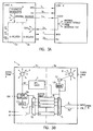
- Fig. 3A shows that the phase alignment means 3 is split into parts 3a and 3b which are related to different clock domains. Whereas part 3a is related to the internal clock A (internal clock on A-side of the phase alignment means), is part 3b related to internal clock B (internal clock on B-side of the phase alignment means).
- the clock generation takes place by a clock generator 4 only in unit A. All clock pulses necessary to control unit A or unit B are derived from the (master) clock pulses of clock generator 4. If necessary the clocks are distributed by various clock distributors 8, 9, 11 - 14 within the units A-E to the units internal circuitry.
- All data AD and control signals AC leaving part 3a of the phase alignment means 3 are aligned with the internal clock of unit A.
- Another signal IGN which is derived from the phase alignment means 3 is used to characterize signals leaving the phase alignment means as being invalid. This ignore signal IGN will be described in greater detail in connection with Figs. 3B and Figs. 4A-E.
- phase alignment buffer An important part of the quasi-synchronous interface is the phase alignment buffer. This section describes one possible implementation of the buffer, however, other implementations are possible and the choice is largely implementation dependent.
- the buffer chosen to be described here is designed to meet the requirements of an on-chip buffer which has a minimum latency and does not have an interruptible data stream. This means that once the system is initialized and a data stream starts, it is not interrupted under normal circumstances even for one cycle. A defect in the system such as the cable from unit A to unit B becoming disconnected would be an error condition and not a normal circumstance.
- both the signals on the data 2 and control 2b lines from unit B to the phase alignment buffer 3 are merged together and treated as data and passed through an input selector 5 into a particular location I-N in the buffer array 6.
- This location is defined by the contents of a WRITE pointer stored in 15 which acts as an address pointer onto the locations of the buffer array.
- the WRITE pointer is updated (e.g.incremented) by adder 10 on every clock cycle which comes across the interface from unit B. Its value is passed to the other side 3a using metastability prevention compensation techniques (MS logic) 7 for comparison with a READ pointer.
- MS logic metastability prevention compensation techniques
- the array has the property of being able to be written with one clock (from B) and read under control of a second different clock (from A).
- buffer locations I-N are read on every clock cycle from the internal clock from unit A. Reading outputs the interface conditions written in by the B side with a given offset of time.
- the READ pointer stored in 17 chooses the array location to be gated onto the read side data and control lines which are fed into the receive logic of unit A.
- the READ pointer also wraps around itself when it reaches the last address of the array, just like the WRITE pointer does.
- Data AD and control AC lines leaving the phase buffer 3 via multiplexer 18 and going to the receive logic of unit A are exactly synchronized both in frequency and phase to unit A's clock because they are read out of the array using unit A's internal clock. When both the READ and WRITE pointers reach the end of the buffer array 6, they wrap around to the first buffer location.
- Metastability (MS) logic 7 and Read Control Logic 16 are used to determine whether the information stored in the currently indicated buffer is valid or not, and whether to advance the READ pointer or not. Buffer contents becomes invalid if the write side clock stops for any reason (controlled stop, error stop) while the read side clock is still running.
- This control logic resides on unit A's clock domain. It is broken into two parts. The first part 7 captures a valid copy of the WRITE pointer into the same clock domain as the READ pointer (on unit A's internal clock). The second part 16 uses this copy of the WRITE pointer to decide the validity of the buffer contents and whether to increment the READ pointer. The WRITE pointer must always be ahead of the READ pointer. If both point to the same buffer location, the read output becomes invalid and has to be ignored by the unit A receive logic.
- the read control logic 16 is used to determine the data validity and advancing of the READ pointer as follows:
- the IGNORE line becomes active it means that the write side of the phase buffer did not receive a clock from unit B. This can happen in two situations. The first case is when the system is initializing and the clocks which have left unit A are still propagating through unit B and back into the phase buffer of unit A. Until the first clock reaches the phase buffer WRITE pointer, IGNORE will be active. The second case is when the path from A to B to phase buffer 3 was broken somewhere. In either case the receive logic in unit A should treat both the data and control lines leaving the phase buffer as invalid until the IGNORE line becomes inactive.
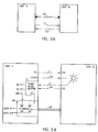
- Figs. 5A, B show how the bidirectional lines 20 must be split on unit A.
- Unit B sees no difference in its implementation of the bidirectional control logic.
- unit A has a special switch function 23 built in around the normal phase alignment buffer 3.
- unit A When unit A is in receive mode (switch in position R), the data path 20 is gated such that data coming from the interface from unit B is routed through the phase buffer 3 before entering unit A's receive logic.
- unit A When unit A is in send mode (switch in position S), the unit A's output path is connected directly to the interface to unit B.
- NOP no operation
- NOP no operation
- NOP cycles When in switching modes, a number of NOP cycles should be performed by unit A's receive logic since the data path through the phase buffer must be reestablished with valid data before normal data processing can start.
- the number of NOP cycles is implementation dependant.
- data is used to refer to the signals which are bidirectional in nature and control to refer to the signals which are unidirectional.
- the terms data and control were chosen for the purposes of illustration as this is how a typical bidirectional interface is implemented.
- Bidirectional signals can also have control functions, likewise unidirectional signals can have data functions.
- Other implementations of handling bidirectional interfaces are possible; this is only one particular example used for illustration purposes.
- WRITE pointer is designated W.
- a series of delays ⁇ is used to make four different copies F, G, H, J of the contents of the WRITE pointer.
- the value of ⁇ should be strictly chosen by the relationship ⁇ >D max , D max being a maximal drift, caused by changes in temperature, threshold values, edge slope and noise, interference, ground and voltage shifts etc.. Accordingly, ⁇ should be less than 1/3 clock cycle.
- Fig.4A shows the WRITE pointer W on the interface clock domain IFD being sent across clock boundary CB to the internal clock domain IND of unit A and being captured in registers F,G,H, and J within MS-LOGIC 7 with a delay ⁇ between F and G, G and H, H and J.
- Fig.4B shows the relative positions of the copies of the contents of W in timing diagram format.
- data arriving at F is exactly aligned with the changes happening in W (not counting physical delays in the implementation of the circuit).
- Data arriving at G is delayed in time by 1 ⁇ , at H by 2 ⁇ , and at J by 3 ⁇ .
- the IND clock will latch all four copies at one time, thus the contents of registers F,G,H,J represent the value of W at different times.
- Fig.4C is the same picture redrawn showing the delays ⁇ at different capturing points for F,G,H,J even though in reality all four are being latched simultaneously.
- the relationship between F,G,H,J is fixed due to the delays ⁇ (J is the oldest copy of W, F is the newest) however the actual contents of each varies based on the alignment between unit A's internal clock and the interface clock. This alignment is covered in the next figure which also brings in the concept of "drift".
- Fig.4D varies the relationships between the read side clock and the write side clock by moving the point where the write side clock changes data in the WRITE pointer.
- the point where the write clock occurs is shown as a bar with a center point, not just a point. This is due to what is defined as "drift" for the purposes of this description.
- the “drift” is the amount of change which can be expected in the write clock edge, relative to the very first clock edge received by the phase alignment buffer. Over time, one would not expect the trigger point of the WRITE pointer to remain the same because things such as temperature changes, threshold changes, clock edge slope changes, noise, interference, ground and voltage shifts, etc. can all affect the point of WRITE pointer triggering. One would expect that this time is small, however, it is not negligible and the value of the delays ⁇ must be chosen to be larger than the maximum possible drift one can expect over the system lifetime. The value of this drift is highly implementation dependant, however for this purposes it is assumed that it is in the 2-3 nanosecond range. Therefore, the value chosen for the delay ⁇ should be greater than 3 nanoseconds. The value must not be larger than 1/3 the cycle time, however, so that all four copies of the WRITE pointer are valid each cycle.
- a logic function is implemented in Fig. 3B on the read side clock domain to provide a stable copy of the WRITE pointer to the read side clock domain.
- the reduced function is as follows.
Landscapes
- Engineering & Computer Science (AREA)
- Theoretical Computer Science (AREA)
- Physics & Mathematics (AREA)
- General Engineering & Computer Science (AREA)
- General Physics & Mathematics (AREA)
- Computer Networks & Wireless Communication (AREA)
- Signal Processing (AREA)
- Information Transfer Systems (AREA)
- Synchronisation In Digital Transmission Systems (AREA)
- Memory System (AREA)
Claims (4)
- Procédé de cadencement de transfert quasi-synchrone de signaux de données et/ou de commande entre deux unités de traitement de données ou plus,
dans lequel les impulsions d'horloge d'une unité maître (UNIT A), passent en même temps que les données et/ou les impulsions de commande présentant la même fréquence et la même phase que lesdites impulsions d'horloge depuis ladite unité maître sur un canal synchrone unidirectionnel (1, 1a) vers une unité voisine (UNIT B),
dans lequel les impulsions d'horloge transférées définissent l'horloge ou les horloges locale(s),
dans lequel en outre les signaux de cadencement, de données, et/ou de commande reviennent sur un canal unidirectionnel (2, 2a) depuis ladite unité voisine vers ladite unité maître,
dans lequel lesdits signaux se produisent à la même fréquence mais avec un décalage de phase, et
dans lequel ledit décalage de phase est compensé par un moyen d'alignement de phase (3) par l'intermédiaire duquel ledit canal unidirectionnel (2, 2a) est relié à ladite unité maître,
dans lequel ledit moyen d'alignement de phase (3) règle les signaux de données, et/ou de commande reçus depuis l'unité voisine à exactement la phase de l'unité maître d'origine, lesquels signaux forment les signaux de données et/ou de commande alignés (AD, AC) pour une utilisation ultérieure, et
dans lequel lesdits signaux de données et/ou de commande reçus sont appliqués à un tableau de mémoires tampons (6-figure 3B), caractérisé en outre par les étapes suivantes :- l'entrée desdits signaux dans ledit tableau de mémoires tampons est commandée par un pointeur d'écriture W lequel est incrémenté à chaque fois qu'une impulsion d'horloge est reçue de l'unité voisine B,- lesdits signaux de données et de commande sont fusionnés ensemble et mémorisés dans lesdites cellules de mémoire tampon indiquées par ledit pointeur d'écriture,- ledit pointeur d'écriture passe en tant que copie d'écriture WC vers une logique de commande de lecture (16) de ladite mémoire tampon par l'intermédiaire d'une logique d'empêchement d'état métastable (7) afin d'être comparé à un pointeur de lecture R lequel indique les cellules de mémoire tampon à partir desquelles les signaux de données et/ou de commande alignés (AD, AC) sont lus, dans lesquels ladite logique d'empêchement d'état métastable et ladite logique de commande de lecture sont utilisées pour déterminer si les informations mémorisées dans les cellules de mémoire tampon actuellement indiquées sont valides ou non, et si l'on doit ou non avancer le pointeur de lecture, et- lorsqu'à la fois ledit pointeur d'écriture et ledit pointeur de lecture atteignent la fin de ladite mémoire tampon, ils recommencent un cycle vers les premières cellules de mémoire tampon (I). - Procédé selon la revendication 1, comprenant en outre les étapes suivantes :- ladite logique d'empêchement d'état métastable (7) laquelle est utilisée pour obtenir une copie d'écriture stable WC en franchissant la limite d'horloge entre l'horloge de l'unité maître et l'horloge en provenance de l'unité voisine sur chaque cycle d'horloge introduit une série de retards , dans lequel Dmax > > 1/3 d'un cycle d'horloge et Dmax étant la dérive maximale de l'horloge reçue depuis l'unité voisine, afin de procurer au moins quatre copies d'écriture différentes F, G, H, J lesquelles seront mémorisées par les impulsions de l'horloge de l'unité maître en une seule fois dans les registres respectifs dans ladite logique d'état métastable (7) représentant ledit pointeur d'écriture à quatre instants différents et- effectuer la fonction suivante afin de procurer une copie d'écriture stable WC à ladite logique de commande de lecture (16) :
lors de l'initialisation, le pointeur de lecture R correspond à chacune des copies d'écriture F, G, H, J respectivement,
WC est établi égal F, jusqu'à ce que R et F correspondent, et ensuite
WC est établi égal H, si G, H et J correspondent également l'un à l'autre, sinon il est établit égal F, et
à partir de ce point, WC provient toujours de cette copie de W. - Procédé selon la revendication 2, comprenant en outre les étapes suivantes :
- un signal de rejet IGN, lequel indique que des données invalides sont reçues d'une unité voisine (B), est généré par la logique de commande de lecture (16) en effectuant la fonction suivante :
si R et WC correspondent, alors IGN est activé et R reste le même, sinon IGN est désactivé, et R est incrémenté. - Agencement destiné à effectuer un procédé selon l'une quelconque des revendications précédentes 1 à 3, comprenant
deux unités de traitement de données ou plus, dans lesquelles une unité maître (UNIT A) comprend une horloge interne,
un canal synchrone unidirectionnel (1, 1a) allant de ladite unité maître à une unité voisine (UNIT B) et vice versa un canal unidirectionnel (2, 2a),
un moyen d'alignement de phase (3) par l'intermédiaire duquel ledit canal unidirectionnel (2, 2a) est relié à ladite unité maître
comprenant
un tableau de mémoires tampons (6) comportant une pluralité de registres afin de mémoriser temporairement des signaux de données et/ou de commande provenant de l'unité voisine (UNIT B) associé au moyen d'alignement de phase, caractérisé par
les registres qui sont reliés par l'intermédiaire d'un sélecteur d'adresse (5) au second canal unidirectionnel (2, 2b) ou lorsque l'on utilise un canal bidirectionnel (20) à la place des deux canaux unidirectionnels, étant relié par l'intermédiaire d'un commutateur (23) à ce canal bidirectionnel,
des circuits d'écriture de tableau de mémoires tampons comportant un moyen de progression d'adresse (10, 15) destiné à commander ledit sélecteur d'adresse, le moyen de progression d'adresse progressant avec les impulsions d'horloge de ladite unité voisine associée,
des circuits de lecture de tableau de mémoires tampons comportant un moyen de progression d'adresse (16, 17, 18) commandés par les impulsions d'horloge maître de ladite unité maître, et
une logique d'empêchement d'état métastable (7) reliée entre lesdits circuits d'écriture de tableau de mémoires tampons et lesdits circuits de lecture de tableau de mémoires tampons afin de détecter et d'indiquer des données erronées qui doivent être rejetées.
Priority Applications (5)
| Application Number | Priority Date | Filing Date | Title |
|---|---|---|---|
| DE69115898T DE69115898T2 (de) | 1991-07-20 | 1991-07-20 | Quasisynchronen Informationsübertragung mit Phasenausgleichvorrichtung |
| EP91112177A EP0525221B1 (fr) | 1991-07-20 | 1991-07-20 | Transfert d'information quasi-synchrone avec dispositif d'alignement de phase |
| JP4151694A JPH0756616B2 (ja) | 1991-07-20 | 1992-06-11 | 信号転送方法及び信号転送装置 |
| CA002074008A CA2074008A1 (fr) | 1991-07-20 | 1992-07-16 | Transfert d'informations quasi-synchrone et dispositif d'alignement de phase connexe |
| US07/916,319 US5450572A (en) | 1991-07-20 | 1992-07-17 | Quasi-synchronous information transfer and phase alignment means for enabling same |
Applications Claiming Priority (1)
| Application Number | Priority Date | Filing Date | Title |
|---|---|---|---|
| EP91112177A EP0525221B1 (fr) | 1991-07-20 | 1991-07-20 | Transfert d'information quasi-synchrone avec dispositif d'alignement de phase |
Publications (2)
| Publication Number | Publication Date |
|---|---|
| EP0525221A1 EP0525221A1 (fr) | 1993-02-03 |
| EP0525221B1 true EP0525221B1 (fr) | 1995-12-27 |
Family
ID=8206961
Family Applications (1)
| Application Number | Title | Priority Date | Filing Date |
|---|---|---|---|
| EP91112177A Expired - Lifetime EP0525221B1 (fr) | 1991-07-20 | 1991-07-20 | Transfert d'information quasi-synchrone avec dispositif d'alignement de phase |
Country Status (5)
| Country | Link |
|---|---|
| US (1) | US5450572A (fr) |
| EP (1) | EP0525221B1 (fr) |
| JP (1) | JPH0756616B2 (fr) |
| CA (1) | CA2074008A1 (fr) |
| DE (1) | DE69115898T2 (fr) |
Cited By (1)
| Publication number | Priority date | Publication date | Assignee | Title |
|---|---|---|---|---|
| WO2007059443A3 (fr) * | 2005-11-10 | 2007-07-26 | Qualcomm Inc | Techniques de generation de signal d'horloge pour memoires ne generant pas de strobe |
Families Citing this family (25)
| Publication number | Priority date | Publication date | Assignee | Title |
|---|---|---|---|---|
| US5634041A (en) * | 1992-08-12 | 1997-05-27 | Massachusetts Institute Of Technology | Rationally clocked communication interface |
| DE4314058A1 (de) * | 1993-04-29 | 1994-11-03 | Bayerische Motoren Werke Ag | Schnittstelle |
| JPH08221315A (ja) | 1995-02-15 | 1996-08-30 | Hitachi Ltd | 情報処理装置 |
| US5822571A (en) * | 1996-06-05 | 1998-10-13 | Compaq Computer Corporation | Synchronizing data between devices |
| US5799175A (en) * | 1996-07-01 | 1998-08-25 | Sun Microsystems, Inc. | Synchronization system and method for plesiochronous signaling |
| US5974103A (en) * | 1996-07-01 | 1999-10-26 | Sun Microsystems, Inc. | Deterministic exchange of data between synchronised systems separated by a distance |
| US6222380B1 (en) * | 1998-06-15 | 2001-04-24 | International Business Machines Corporation | High speed parallel/serial link for data communication |
| US6499113B1 (en) | 1999-08-31 | 2002-12-24 | Sun Microsystems, Inc. | Method and apparatus for extracting first failure and attendant operating information from computer system devices |
| US6546507B1 (en) | 1999-08-31 | 2003-04-08 | Sun Microsystems, Inc. | Method and apparatus for operational envelope testing of busses to identify halt limits |
| US6473871B1 (en) | 1999-08-31 | 2002-10-29 | Sun Microsystems, Inc. | Method and apparatus for HASS testing of busses under programmable control |
| US6535945B1 (en) | 1999-08-31 | 2003-03-18 | Sun Microsystems, Inc. | Method and apparatus for programmable adjustment of computer system bus parameters |
| US6609221B1 (en) | 1999-08-31 | 2003-08-19 | Sun Microsystems, Inc. | Method and apparatus for inducing bus saturation during operational testing of busses using a pattern generator |
| US6502212B1 (en) | 1999-08-31 | 2002-12-31 | Sun Microsystems, Inc. | Method and apparatus for bus parameter optimization using probes of system configurations |
| US6275077B1 (en) | 1999-08-31 | 2001-08-14 | Sun Microsystems, Inc. | Method and apparatus for programmable adjustment of bus driver propagation times |
| US6321282B1 (en) | 1999-10-19 | 2001-11-20 | Rambus Inc. | Apparatus and method for topography dependent signaling |
| US6987823B1 (en) * | 2000-02-07 | 2006-01-17 | Rambus Inc. | System and method for aligning internal transmit and receive clocks |
| US6898726B1 (en) * | 2000-11-15 | 2005-05-24 | Micron Technology, Inc. | Memory system that sets a predetermined phase relationship between read and write clock signals at a bus midpoint for a plurality of spaced device locations |
| JP2002183692A (ja) * | 2000-12-14 | 2002-06-28 | Sony Corp | Icカードおよびicカードシステム |
| JP3604372B2 (ja) | 2002-02-18 | 2004-12-22 | 沖電気工業株式会社 | シンクロナスdram制御回路 |
| US7477713B2 (en) * | 2004-03-02 | 2009-01-13 | International Business Machines Corporation | method for providing automatic adaptation to frequency offsets in high speed serial links |
| JP2006146430A (ja) * | 2004-11-17 | 2006-06-08 | Olympus Corp | データ入出力装置、データ入出力システム、及びデータ通信方法 |
| EP2026493A1 (fr) * | 2007-08-16 | 2009-02-18 | STMicroelectronics S.r.l. | Procédé et systèmes de communication mésochrone dans des domaines d'horloge multiples et produit de programme informatique correspondant |
| US20180293025A1 (en) * | 2014-11-10 | 2018-10-11 | Sony Corporation | Interface circuit, memory device, information processing system, and interface circuit controlling method |
| US9946672B2 (en) * | 2015-08-28 | 2018-04-17 | Cirrus Logic, Inc. | Transfer for control data over half-duplex link |
| CN119902600B (zh) * | 2025-03-31 | 2025-07-18 | 成都九洲迪飞科技有限责任公司 | 基于fpga的ad采样系统内外相位同步方法、系统和电子设备 |
Family Cites Families (15)
| Publication number | Priority date | Publication date | Assignee | Title |
|---|---|---|---|---|
| US3588703A (en) * | 1967-05-01 | 1971-06-28 | Trw Inc | Phase synchronization system |
| US3970997A (en) * | 1974-08-29 | 1976-07-20 | Honeywell Information Systems, Inc. | High speed peripheral system interface |
| JPS5151247A (ja) * | 1974-10-31 | 1976-05-06 | Fujitsu Ltd | Kurotsukuisochoseihoho |
| US4119796A (en) * | 1976-11-01 | 1978-10-10 | Versitron, Inc. | Automatic data synchronizer |
| US4208724A (en) * | 1977-10-17 | 1980-06-17 | Sperry Corporation | System and method for clocking data between a remote unit and a local unit |
| US4677614A (en) * | 1983-02-15 | 1987-06-30 | Emc Controls, Inc. | Data communication system and method and communication controller and method therefor, having a data/clock synchronizer and method |
| US4596026A (en) * | 1983-05-09 | 1986-06-17 | Raytheon Company | Asynchronous data clock generator |
| US4637018A (en) * | 1984-08-29 | 1987-01-13 | Burroughs Corporation | Automatic signal delay adjustment method |
| DE3584751D1 (de) * | 1984-09-21 | 1992-01-09 | Amt Holdings | Datenuebertragungssystem. |
| US4873703A (en) * | 1985-09-27 | 1989-10-10 | Hewlett-Packard Company | Synchronizing system |
| US4782499A (en) * | 1986-09-29 | 1988-11-01 | Rockwell International Corporation | Automatic alignment of a synchronous data system using a local reference clock and external clock with an unknown delay between the two clocks |
| US4881165A (en) * | 1988-04-01 | 1989-11-14 | Digital Equipment Corporation | Method and apparatus for high speed data transmission between two systems operating under the same clock with unknown and non constant skew in the clock between the two systems |
| US5208913A (en) * | 1988-06-22 | 1993-05-04 | Sharp Kabushiki Kaisha | Buffer memory for synchronizing data transmission and reception between two devices having mutually different operating speeds and operating methods therefor |
| US4943984A (en) * | 1988-06-24 | 1990-07-24 | International Business Machines Corporation | Data processing system parallel data bus having a single oscillator clocking apparatus |
| NL9002426A (nl) * | 1990-11-08 | 1992-06-01 | Koninkl Philips Electronics Nv | Elastisch buffergeheugen. |
-
1991
- 1991-07-20 DE DE69115898T patent/DE69115898T2/de not_active Expired - Fee Related
- 1991-07-20 EP EP91112177A patent/EP0525221B1/fr not_active Expired - Lifetime
-
1992
- 1992-06-11 JP JP4151694A patent/JPH0756616B2/ja not_active Expired - Lifetime
- 1992-07-16 CA CA002074008A patent/CA2074008A1/fr not_active Abandoned
- 1992-07-17 US US07/916,319 patent/US5450572A/en not_active Expired - Fee Related
Cited By (3)
| Publication number | Priority date | Publication date | Assignee | Title |
|---|---|---|---|---|
| WO2007059443A3 (fr) * | 2005-11-10 | 2007-07-26 | Qualcomm Inc | Techniques de generation de signal d'horloge pour memoires ne generant pas de strobe |
| US7656743B2 (en) | 2005-11-10 | 2010-02-02 | Qualcomm, Incorporated | Clock signal generation techniques for memories that do not generate a strobe |
| CN101356514B (zh) * | 2005-11-10 | 2010-09-15 | 高通股份有限公司 | 时钟电路、用于产生时钟信号的方法及存储器系统 |
Also Published As
| Publication number | Publication date |
|---|---|
| US5450572A (en) | 1995-09-12 |
| DE69115898D1 (de) | 1996-02-08 |
| CA2074008A1 (fr) | 1993-01-21 |
| EP0525221A1 (fr) | 1993-02-03 |
| JPH0756616B2 (ja) | 1995-06-14 |
| DE69115898T2 (de) | 1996-07-11 |
| JPH05189081A (ja) | 1993-07-30 |
Similar Documents
| Publication | Publication Date | Title |
|---|---|---|
| EP0525221B1 (fr) | Transfert d'information quasi-synchrone avec dispositif d'alignement de phase | |
| US7747888B2 (en) | Technique to create link determinism | |
| US5509038A (en) | Multi-path data synchronizer system and method | |
| US5644604A (en) | Digital phase selector system and method | |
| US7242736B2 (en) | Data transfer | |
| EP0606600B1 (fr) | Concepts de FIFO à un ou plusieurs étages améliorées pour des synchronisateurs de transfert de données | |
| US20090323728A1 (en) | Asynchronous data fifo that provides uninterrupted data flow | |
| EP3871062B1 (fr) | Asic asynchrone | |
| US6977979B1 (en) | Enhanced clock forwarding data recovery | |
| JPH07112184B2 (ja) | デジタル・データ転送回路 | |
| US7739538B2 (en) | Double data rate chaining for synchronous DDR interfaces | |
| US20060280274A1 (en) | Receiving apparatus, data transmission system and receiving method | |
| US7454538B2 (en) | Latency insensitive FIFO signaling protocol | |
| US7783911B2 (en) | Programmable bus driver launch delay/cycle delay to reduce elastic interface elasticity requirements | |
| US20080147916A1 (en) | Data synchronization method of data buffer device | |
| US9880961B2 (en) | Asynchronous bridge circuitry and a method of transferring data using asynchronous bridge circuitry | |
| EP1317085B1 (fr) | Procédé et circuit d'initialisation de mémoire tampon pour compensation de délai dans un système à signal d'horloge transmis | |
| US5355504A (en) | Self-synchronizing data queues | |
| US6067629A (en) | Apparatus and method for pseudo-synchronous communication between clocks of different frequencies | |
| US5928375A (en) | Method for enhancing data transmission in parity based data processing systems | |
| US6055588A (en) | Single stage FIFO memory with a circuit enabling memory to be read from and written to during a single cycle from a single clock | |
| US6016521A (en) | Communication control device | |
| JP2001060977A (ja) | 伝送システム | |
| US7328361B2 (en) | Digital bus synchronizer for generating read reset signal | |
| JPH02262739A (ja) | 双方向リンクを介して情報を伝送する方法と、この方法を実施するための装置 |
Legal Events
| Date | Code | Title | Description |
|---|---|---|---|
| PUAI | Public reference made under article 153(3) epc to a published international application that has entered the european phase |
Free format text: ORIGINAL CODE: 0009012 |
|
| AK | Designated contracting states |
Kind code of ref document: A1 Designated state(s): BE CH DE FR GB IT LI NL SE |
|
| 17P | Request for examination filed |
Effective date: 19930519 |
|
| 17Q | First examination report despatched |
Effective date: 19931029 |
|
| GRAA | (expected) grant |
Free format text: ORIGINAL CODE: 0009210 |
|
| AK | Designated contracting states |
Kind code of ref document: B1 Designated state(s): BE CH DE FR GB IT LI NL SE |
|
| PG25 | Lapsed in a contracting state [announced via postgrant information from national office to epo] |
Ref country code: NL Free format text: LAPSE BECAUSE OF FAILURE TO SUBMIT A TRANSLATION OF THE DESCRIPTION OR TO PAY THE FEE WITHIN THE PRESCRIBED TIME-LIMIT Effective date: 19951227 Ref country code: LI Effective date: 19951227 Ref country code: CH Effective date: 19951227 Ref country code: BE Effective date: 19951227 |
|
| ITF | It: translation for a ep patent filed | ||
| REF | Corresponds to: |
Ref document number: 69115898 Country of ref document: DE Date of ref document: 19960208 |
|
| REG | Reference to a national code |
Ref country code: CH Ref legal event code: NV Representative=s name: CARL O. BARTH C/O IBM CORPORATION ZURICH INTELLECT |
|
| ET | Fr: translation filed | ||
| PG25 | Lapsed in a contracting state [announced via postgrant information from national office to epo] |
Ref country code: SE Effective date: 19960327 |
|
| NLV1 | Nl: lapsed or annulled due to failure to fulfill the requirements of art. 29p and 29m of the patents act | ||
| PGFP | Annual fee paid to national office [announced via postgrant information from national office to epo] |
Ref country code: GB Payment date: 19960621 Year of fee payment: 6 |
|
| PGFP | Annual fee paid to national office [announced via postgrant information from national office to epo] |
Ref country code: DE Payment date: 19960724 Year of fee payment: 6 |
|
| PLBE | No opposition filed within time limit |
Free format text: ORIGINAL CODE: 0009261 |
|
| STAA | Information on the status of an ep patent application or granted ep patent |
Free format text: STATUS: NO OPPOSITION FILED WITHIN TIME LIMIT |
|
| 26N | No opposition filed | ||
| PG25 | Lapsed in a contracting state [announced via postgrant information from national office to epo] |
Ref country code: FR Effective date: 19970328 |
|
| REG | Reference to a national code |
Ref country code: FR Ref legal event code: ST |
|
| PG25 | Lapsed in a contracting state [announced via postgrant information from national office to epo] |
Ref country code: GB Free format text: LAPSE BECAUSE OF NON-PAYMENT OF DUE FEES Effective date: 19970720 |
|
| GBPC | Gb: european patent ceased through non-payment of renewal fee |
Effective date: 19970720 |
|
| PG25 | Lapsed in a contracting state [announced via postgrant information from national office to epo] |
Ref country code: DE Free format text: LAPSE BECAUSE OF NON-PAYMENT OF DUE FEES Effective date: 19980401 |
|
| PG25 | Lapsed in a contracting state [announced via postgrant information from national office to epo] |
Ref country code: IT Free format text: LAPSE BECAUSE OF NON-PAYMENT OF DUE FEES Effective date: 20050720 |