EP0525385B1 - Supraconducteur céramique à haute, température, stabilisé et son procédé de préparation - Google Patents
Supraconducteur céramique à haute, température, stabilisé et son procédé de préparation Download PDFInfo
- Publication number
- EP0525385B1 EP0525385B1 EP92110645A EP92110645A EP0525385B1 EP 0525385 B1 EP0525385 B1 EP 0525385B1 EP 92110645 A EP92110645 A EP 92110645A EP 92110645 A EP92110645 A EP 92110645A EP 0525385 B1 EP0525385 B1 EP 0525385B1
- Authority
- EP
- European Patent Office
- Prior art keywords
- temperature superconductor
- die
- superconductor
- stage
- metallic conductor
- Prior art date
- Legal status (The legal status is an assumption and is not a legal conclusion. Google has not performed a legal analysis and makes no representation as to the accuracy of the status listed.)
- Expired - Lifetime
Links
- 239000002887 superconductor Substances 0.000 title claims description 58
- 238000000034 method Methods 0.000 title claims description 16
- 239000000919 ceramic Substances 0.000 title claims description 14
- 238000004519 manufacturing process Methods 0.000 title description 8
- 239000004020 conductor Substances 0.000 claims description 39
- 229910052709 silver Inorganic materials 0.000 claims description 18
- RYGMFSIKBFXOCR-UHFFFAOYSA-N Copper Chemical compound [Cu] RYGMFSIKBFXOCR-UHFFFAOYSA-N 0.000 claims description 15
- 229910052802 copper Inorganic materials 0.000 claims description 15
- 239000010949 copper Substances 0.000 claims description 15
- 239000004332 silver Substances 0.000 claims description 15
- 239000000155 melt Substances 0.000 claims description 12
- 229910044991 metal oxide Inorganic materials 0.000 claims description 11
- 150000004706 metal oxides Chemical class 0.000 claims description 11
- 239000000463 material Substances 0.000 claims description 10
- 229910052751 metal Inorganic materials 0.000 claims description 10
- 239000002184 metal Substances 0.000 claims description 10
- PCHJSUWPFVWCPO-UHFFFAOYSA-N gold Chemical compound [Au] PCHJSUWPFVWCPO-UHFFFAOYSA-N 0.000 claims description 9
- OYPRJOBELJOOCE-UHFFFAOYSA-N Calcium Chemical compound [Ca] OYPRJOBELJOOCE-UHFFFAOYSA-N 0.000 claims description 8
- 229910052797 bismuth Inorganic materials 0.000 claims description 8
- JCXGWMGPZLAOME-UHFFFAOYSA-N bismuth atom Chemical compound [Bi] JCXGWMGPZLAOME-UHFFFAOYSA-N 0.000 claims description 8
- 229910052791 calcium Inorganic materials 0.000 claims description 8
- 239000011575 calcium Substances 0.000 claims description 8
- 229910052737 gold Inorganic materials 0.000 claims description 8
- 239000010931 gold Substances 0.000 claims description 8
- 229910052712 strontium Inorganic materials 0.000 claims description 8
- CIOAGBVUUVVLOB-UHFFFAOYSA-N strontium atom Chemical compound [Sr] CIOAGBVUUVVLOB-UHFFFAOYSA-N 0.000 claims description 8
- 150000002739 metals Chemical class 0.000 claims description 6
- QVGXLLKOCUKJST-UHFFFAOYSA-N atomic oxygen Chemical compound [O] QVGXLLKOCUKJST-UHFFFAOYSA-N 0.000 claims description 5
- 229910052760 oxygen Inorganic materials 0.000 claims description 5
- 239000001301 oxygen Substances 0.000 claims description 5
- 238000010438 heat treatment Methods 0.000 claims description 3
- 229910052741 iridium Inorganic materials 0.000 claims description 3
- 229910052762 osmium Inorganic materials 0.000 claims description 3
- 229910052763 palladium Inorganic materials 0.000 claims description 3
- 239000000843 powder Substances 0.000 claims description 3
- 229910052703 rhodium Inorganic materials 0.000 claims description 3
- 229910052707 ruthenium Inorganic materials 0.000 claims description 3
- 229910045601 alloy Inorganic materials 0.000 claims description 2
- 239000000956 alloy Substances 0.000 claims description 2
- 229910052697 platinum Inorganic materials 0.000 claims description 2
- 238000004528 spin coating Methods 0.000 claims 2
- BQCADISMDOOEFD-UHFFFAOYSA-N Silver Chemical compound [Ag] BQCADISMDOOEFD-UHFFFAOYSA-N 0.000 description 19
- IJGRMHOSHXDMSA-UHFFFAOYSA-N Atomic nitrogen Chemical compound N#N IJGRMHOSHXDMSA-UHFFFAOYSA-N 0.000 description 16
- 239000011159 matrix material Substances 0.000 description 9
- 229910052757 nitrogen Inorganic materials 0.000 description 8
- VYPSYNLAJGMNEJ-UHFFFAOYSA-N Silicium dioxide Chemical compound O=[Si]=O VYPSYNLAJGMNEJ-UHFFFAOYSA-N 0.000 description 6
- 230000006378 damage Effects 0.000 description 6
- 239000000203 mixture Substances 0.000 description 6
- AZUYLZMQTIKGSC-UHFFFAOYSA-N 1-[6-[4-(5-chloro-6-methyl-1H-indazol-4-yl)-5-methyl-3-(1-methylindazol-5-yl)pyrazol-1-yl]-2-azaspiro[3.3]heptan-2-yl]prop-2-en-1-one Chemical compound ClC=1C(=C2C=NNC2=CC=1C)C=1C(=NN(C=1C)C1CC2(CN(C2)C(C=C)=O)C1)C=1C=C2C=NN(C2=CC=1)C AZUYLZMQTIKGSC-UHFFFAOYSA-N 0.000 description 5
- 239000010453 quartz Substances 0.000 description 5
- 230000006641 stabilisation Effects 0.000 description 5
- 238000011105 stabilization Methods 0.000 description 5
- 239000010970 precious metal Substances 0.000 description 4
- 239000007787 solid Substances 0.000 description 4
- 238000003466 welding Methods 0.000 description 4
- 230000015556 catabolic process Effects 0.000 description 3
- 238000009750 centrifugal casting Methods 0.000 description 3
- 239000011248 coating agent Substances 0.000 description 3
- 238000000576 coating method Methods 0.000 description 3
- 230000000052 comparative effect Effects 0.000 description 3
- 238000001816 cooling Methods 0.000 description 3
- 238000006731 degradation reaction Methods 0.000 description 3
- 230000000694 effects Effects 0.000 description 3
- 238000002844 melting Methods 0.000 description 3
- 230000008018 melting Effects 0.000 description 3
- 229910000510 noble metal Inorganic materials 0.000 description 3
- 238000005253 cladding Methods 0.000 description 2
- 239000002131 composite material Substances 0.000 description 2
- 239000007788 liquid Substances 0.000 description 2
- 229910001092 metal group alloy Inorganic materials 0.000 description 2
- 238000000465 moulding Methods 0.000 description 2
- 229910001257 Nb alloy Inorganic materials 0.000 description 1
- 244000089486 Phragmites australis subsp australis Species 0.000 description 1
- 229910001069 Ti alloy Inorganic materials 0.000 description 1
- ATJFFYVFTNAWJD-UHFFFAOYSA-N Tin Chemical compound [Sn] ATJFFYVFTNAWJD-UHFFFAOYSA-N 0.000 description 1
- RTAQQCXQSZGOHL-UHFFFAOYSA-N Titanium Chemical compound [Ti] RTAQQCXQSZGOHL-UHFFFAOYSA-N 0.000 description 1
- 238000005266 casting Methods 0.000 description 1
- 238000010276 construction Methods 0.000 description 1
- 229910052758 niobium Inorganic materials 0.000 description 1
- 239000010955 niobium Substances 0.000 description 1
- GUCVJGMIXFAOAE-UHFFFAOYSA-N niobium atom Chemical compound [Nb] GUCVJGMIXFAOAE-UHFFFAOYSA-N 0.000 description 1
- 239000012255 powdered metal Substances 0.000 description 1
- 238000004544 sputter deposition Methods 0.000 description 1
- 230000000087 stabilizing effect Effects 0.000 description 1
- 239000010935 stainless steel Substances 0.000 description 1
- 229910001220 stainless steel Inorganic materials 0.000 description 1
- 239000010936 titanium Substances 0.000 description 1
Images
Classifications
-
- C—CHEMISTRY; METALLURGY
- C04—CEMENTS; CONCRETE; ARTIFICIAL STONE; CERAMICS; REFRACTORIES
- C04B—LIME, MAGNESIA; SLAG; CEMENTS; COMPOSITIONS THEREOF, e.g. MORTARS, CONCRETE OR LIKE BUILDING MATERIALS; ARTIFICIAL STONE; CERAMICS; REFRACTORIES; TREATMENT OF NATURAL STONE
- C04B35/00—Shaped ceramic products characterised by their composition; Ceramics compositions; Processing powders of inorganic compounds preparatory to the manufacturing of ceramic products
- C04B35/01—Shaped ceramic products characterised by their composition; Ceramics compositions; Processing powders of inorganic compounds preparatory to the manufacturing of ceramic products based on oxide ceramics
- C04B35/45—Shaped ceramic products characterised by their composition; Ceramics compositions; Processing powders of inorganic compounds preparatory to the manufacturing of ceramic products based on oxide ceramics based on copper oxide or solid solutions thereof with other oxides
-
- C—CHEMISTRY; METALLURGY
- C04—CEMENTS; CONCRETE; ARTIFICIAL STONE; CERAMICS; REFRACTORIES
- C04B—LIME, MAGNESIA; SLAG; CEMENTS; COMPOSITIONS THEREOF, e.g. MORTARS, CONCRETE OR LIKE BUILDING MATERIALS; ARTIFICIAL STONE; CERAMICS; REFRACTORIES; TREATMENT OF NATURAL STONE
- C04B35/00—Shaped ceramic products characterised by their composition; Ceramics compositions; Processing powders of inorganic compounds preparatory to the manufacturing of ceramic products
- C04B35/622—Forming processes; Processing powders of inorganic compounds preparatory to the manufacturing of ceramic products
- C04B35/653—Processes involving a melting step
-
- C—CHEMISTRY; METALLURGY
- C04—CEMENTS; CONCRETE; ARTIFICIAL STONE; CERAMICS; REFRACTORIES
- C04B—LIME, MAGNESIA; SLAG; CEMENTS; COMPOSITIONS THEREOF, e.g. MORTARS, CONCRETE OR LIKE BUILDING MATERIALS; ARTIFICIAL STONE; CERAMICS; REFRACTORIES; TREATMENT OF NATURAL STONE
- C04B35/00—Shaped ceramic products characterised by their composition; Ceramics compositions; Processing powders of inorganic compounds preparatory to the manufacturing of ceramic products
- C04B35/71—Ceramic products containing macroscopic reinforcing agents
- C04B35/78—Ceramic products containing macroscopic reinforcing agents containing non-metallic materials
- C04B35/80—Fibres, filaments, whiskers, platelets, or the like
-
- H—ELECTRICITY
- H10—SEMICONDUCTOR DEVICES; ELECTRIC SOLID-STATE DEVICES NOT OTHERWISE PROVIDED FOR
- H10N—ELECTRIC SOLID-STATE DEVICES NOT OTHERWISE PROVIDED FOR
- H10N60/00—Superconducting devices
- H10N60/20—Permanent superconducting devices
- H10N60/203—Permanent superconducting devices comprising high-Tc ceramic materials
Definitions
- the present invention relates to a ceramic high-temperature superconductor stabilized with metallic conductors and to a method for its production.
- a disadvantage of all previously known high-temperature superconductors is their low mechanical stability, which leads to a low-resistance short circuit in the passage of current if the high-temperature superconductor breaks. There is a risk that the ohmic heat developed at this break point will raise the temperature and make the high-temperature superconductor normally conductive. In the case of a normally conductive high-temperature superconductor, the developed ohmic heat can lead to its complete destruction.
- the so-called degradation effect leads to their destruction when the energy stored in the field is not dissipated.
- the degradation effect means that even with load currents that are smaller by a factor of 2 and more than the expected critical current, instabilities occur which lead to the complete normal conduction of the high-temperature superconductor, cf. Werner Buckel, "Superconductivity", Fundamentals and Applications, 3rd ed. (1984), pages 227 ff.
- This type of stabilization by embedding in a metal matrix is not transferable to solid parts made of high-temperature superconductors based on metal oxide mixtures of bismuth, strontium, calcium and copper, since moldings made from these metal oxide mixtures are too brittle and cannot be deformed mechanically .
- the normal line and thus the destruction of the high-temperature superconductor by the degradation effect should be prevented.
- the object could surprisingly be achieved by leading a metallic conductor parallel to the high-temperature superconductor, the high-temperature superconductor being in contact with the metallic conductor, and the high-temperature superconductor and the metallic conductor having common contact pieces on which the Power connection is made.
- a method for producing the stabilized, ceramic high-temperature superconductor according to the invention can be characterized in that one or more metallic conductors are arranged in a matrix parallel to the longitudinal axis of the matrix, the matrix with the molten metal oxides of bismuth, strontium, calcium and copper in a molar ratio the metals are filled up from 2: 2: 1: 2 and allowed to solidify, the solidified melt is removed from the die and tempered in a first stage at temperatures of 710 to 810 ° C and in a second stage in an oxygen-containing atmosphere at temperatures of 750 to 870 ° C .
- Another method for producing the stabilized ceramic superconductor according to the invention can be characterized in that one or more metallic conductors are arranged in a matrix parallel to the longitudinal axis of the matrix and the matrix is filled with powdered metal oxides or finished superconductor powder and the metal oxides in the matrix completely or partially melted, then tempered in a first stage in an air atmosphere at 710 to 810 ° C and in a second stage in an oxygen-containing atmosphere at 750 to 870 ° C. Silver or gold is used as the matrix material.
- a short-term normal line of a few seconds can destroy the high-temperature superconductor leads.
- a metallic conductor with a cross section of 0.2 mm 2 is completely sufficient for stabilizing a current of 20 A flowing in the high-temperature superconductor.
- the ceramic high-temperature superconductor can be stabilized with metallic conductors in various ways:
- the metallic conductor is completely or partially covered with melt and the entire arrangement is annealed, the superconducting state and good electrical contact between the superconducting material and the metallic conductor being achieved.
- the contact piece required for the actual power supply can be controlled by an independent process such as are made by sputtering gold.
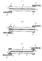
- FIG. 1a An arrangement is then obtained as shown in FIG. 1a.
- the current is dissipated via the wire running centrally through the rod.
- the metallic conductor would be ineffective, since in this arrangement there is no direct connection between the contact piece and the metallic conductor.
- An arrangement as in Fig. 1c is therefore preferable in any case.
- the metallic conductor is arranged parallel outside or inside to the high-temperature superconductor.
- the external arrangement has the disadvantage that the metallic conductor can be torn off mechanically.
- An internal arrangement of the metallic conductor in the high-temperature superconductor should therefore be preferred.
- the internal arrangement of the metallic conductor also gives the high-temperature superconductor increased breaking strength.
- a longitudinal section through a high-temperature superconductor is shown.
- the metallic conductor 3 is arranged in the ceramic high-temperature superconductor material 1.
- the high-temperature superconductor is connected to a circuit via the lead 5 and the contact piece 2.
- 6 illustrates two different possibilities of a break in the ceramic high-temperature superconductor material.
- Fig. 1c is the metallic conductor 3 connected to the contact piece 2 via a welding point 4.
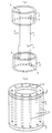
- Fig. 2 shows the spatial representation of a cage, which is formed from the annular contact pieces 2, which are connected to the metallic conductor 3 via the weld 4.
- the cage is filled with ceramic high-temperature superconductor material 1.
- Fig. 3 shows the spatial representation of a cylinder made by the centrifugal casting process made of high-temperature superconductor material, which is provided with two contact pieces 2 made of silver sheet, which are connected to one another via the welding spots 4 and the electrical conductor 3.
- Example 1a (Comparative example of operation according to FIG. 1a)
- Example 1a In a departure from Example 1a, the wires were not guided through the middle of the end faces, but along the bottom of the copper mold, so that the wire was only partially surrounded by the melt or was directly above the surface of the solidified melt.
- the resistance of this wire was 0.7 at room temperature. 10 -3 ⁇ and thus corresponded to the resistance which was determined for this wire before the coating with melt.
- Example 1a the silver wire, which ran through the middle of the slowly solidifying melt, was partially melted or dissolved by the high initial temperature of the melt (1050 ° C.), since the melting point for silver is 950 ° C. In contrast, the melt cooled very quickly near the copper mold wall.
- the wire By arranging the wire in this edge zone of the solid body (as in Example 1a), the reduction in the silver wire cross section under the influence of the melt can be prevented.
- Example 1a was repeated with a 0.5 mm thick gold wire instead of the silver wire.
- the resistance of the wire in the solidified melt was 0.95. 10 -3 ⁇ and thus corresponded exactly to the resistance that was determined for a similar wire outside of the solidified melt.
- the different behavior of the gold wire is due to the higher melting point of the gold (1065 ° C).
- Two rings each 10 mm wide and 8 mm in diameter, were formed from a 0.5 mm thick sheet of silver and connected to one another by spot welding via two silver wires (diameter 0.5 mm, length 100 mm) (FIG. 2).
- This construction was pushed into a quartz glass tube with an internal diameter of 8 mm and a length of 120 mm, which was closed on one side.
- a mixture of the oxides of bismuth, strontium, calcium and copper in the ratio of metals of 2: 2: 1: 2 was heated to 1000 ° C. until a homogeneous melt was formed.
- This melt was poured into the quartz tube prepared in this way, the silver wires being partially enclosed by the melt. After cooling to room temperature, the shaped body was removed from the quartz tube.
- the total resistance of the wires in the solidified melt became 1.2. 10 -3 ⁇ determined and thus corresponded to the resistance before the coating with molten metal oxides.
- the shaped body produced according to Example 2 was heated in a tube furnace under a mixture of air and nitrogen in a ratio of 1: 1 to a heating rate of 300 ° C./h to 750 ° C., and annealed at this temperature for 24 hours. The mixture was then heated to 830 ° C. in an air atmosphere and annealed at 830 ° C. for a further 36 hours.
- the contact resistance between silver and superconductor was to 0.028. 10 -3 ⁇ determined.
- the shaped body produced according to Example 3 was connected to a direct current source and (without an external magnetic field) a direct current of 20 A was passed through the shaped body at the temperature of the liquid nitrogen (77 K). After the molded body was pulled out of the nitrogen bath, the resistance in the molded body suddenly increased to 0.210. 10 -3 ⁇ . Then there was a slow, steady increase in resistance. After 25 seconds the wire had melted and the resistance jumped to 50 again. 10 -3 ⁇ .
- the metallic conductor therefore took over most of the current flow for 25 seconds after being pulled out of the nitrogen bath.
- the example sequence 2, 3, and 4a was repeated with the change that the silver sheet rings were not connected to one another by silver wires. After the molded body was pulled out of the nitrogen bath, the resistance jumped to 55. 10 -3 ⁇ .
- the shaped body obtained was tempered as described in Example 3. Gold contacts were then sputtered onto the ends of the shaped body and were heat-treated at 550 ° C. for 0.5 hours. A current of 20 A was passed through this shaped body at the temperature of the liquid nitrogen. After the sample was pulled out of the nitrogen bath, the resistance in the molded body suddenly increased to 0.405. 10 -3 ⁇ . Then there was a slow, steady increase in resistance. After 35 seconds the wire had melted and the resistance jumped to 65. 10 -3 ⁇ . Again, after the nitrogen cooling ceased to exist, the metallic conductor took over most of the current that originally only flowed in the superconductor for a limited time.
- Spot welding was used to connect two rings made of 0.5 mm thick silver sheet (outer diameter 47 mm, inner diameter 37 mm) to ten silver wires (diameter 0.5 mm, length 200 mm) so that the silver wires were welded to the inside of the rings and formed a cage with the sheets.
- This cage was pushed into a horizontal, cylindrical mold made of thin stainless steel sheet (diameter 50 mm, length 200 mm).
- the mold was rotated at 500 rpm around its longitudinal axis and a melt (melting temperature: 1000 ° C.) of the oxides of bismuth, strontium, Calcium and copper filled in the ratio of metals of 2: 2: 1: 2. Due to the centrifugal force, the melt was quickly and evenly distributed on the mold wall to form a hollow cylinder. After cooling, a hollow cylinder with a wall thickness of 4 mm could be removed from the mold.
- the silver wires were in the outer wall of the hollow cylinder and were partially covered by the solidified melt (Fig. 3).
- the original resistance of the silver conductors was not changed by the coating with the melt.
Landscapes
- Chemical & Material Sciences (AREA)
- Engineering & Computer Science (AREA)
- Ceramic Engineering (AREA)
- Manufacturing & Machinery (AREA)
- Structural Engineering (AREA)
- Materials Engineering (AREA)
- Organic Chemistry (AREA)
- Inorganic Compounds Of Heavy Metals (AREA)
- Chemical Kinetics & Catalysis (AREA)
- Inorganic Chemistry (AREA)
- Superconductors And Manufacturing Methods Therefor (AREA)
- Compositions Of Oxide Ceramics (AREA)
- Superconductor Devices And Manufacturing Methods Thereof (AREA)
Claims (13)
- Supraconducteur à température élevée, céramique, stabilisé, à base d'oxydes métalliques fondus du bismuth, du strontium, du calcium et du cuivre, un conducteur métallique étant introduit parallèlement au supraconducteur à température élevée et le supraconducteur à température élevée étant en contact avec le conducteur métallique, caractérisé en ce que le supraconducteur à température élevée et le conducteur métallique présentent des plots de contact communs sur lesquels se fait le raccordement de courant.
- Supraconducteur à température élevée selon la revendication 1, caractérisé en ce qu'un ou plusieurs conducteurs métalliques relient les plots de contact pour les raccordements de courant.
- Supraconducteur à température élevée selon la revendication 1 ou 2, caractérisé en ce que le conducteur métallique est constitué de métal précieux.
- Supraconducteur à température élevée selon la revendication 3, caractérisé en ce qu'on utilise comme métal précieux Ag, Au, Ru, Os, Rh, Ir, Pd ou Pt ou un alliage contenant ces métaux précieux.
- Supraconducteur à température élevée selon l'une quelconque des revendications 1 à 4, caractérisé en ce que le conducteur métallique est totalement ou partiellement enveloppé du supraconducteur à température élevée.
- Supraconducteur à température élevée selon l'une quelconque des revendications 1 à 5, caractérisé en ce que le supraconducteur à température élevée est préparé à partir des oxydes métalliques fondus dans la forme d'un tube dans un procédé de coulée centrifuge.
- Supraconducteur à température élevée selon l'une quelconque des revendications 1 à 6, caractérisé en ce que les extrémités de tube sont munies dans le procédé de coulée centrifuge de plots de contact annulaires pour le raccordement de courant, les deux plots de contact étant reliés par l'intermédiaire d'un ou plusieurs conducteurs métalliques.
- Procédé pour la préparation de supraconducteurs à température élevée, céramiques, stabilisés selon l'une quelconque des revendications 1 à 7, caractérisé en ce que l'on dispose dans une matrice un ou plusieurs conducteurs métalliques parallèlement à l'axe longitudinal de la matrice et on remplit la matrice avec les oxydes métalliques fondus du bismuth, du strontium, du calcium et du cuivre dans un rapport molaire des métaux de 2 : 2 : 1 : 2 et on laisse solidifier.
- Procédé selon la revendication 8, caractérisé en ce qu'on tempère la masse fondue solidifiée dans une première étape à des températures de 710 à 810°C et dans une deuxième étape dans une atmosphère oxygénée à des températures de 750 à 870°C.
- Procédé pour la préparation de supraconducteurs céramiques stabilisés selon l'une quelconque des revendications 1 à 5, caractérisé en ce que l'on dispose dans une matrice un ou plusieurs conducteurs métalliques parallèlement à l'axe longitudinal de la matrice et on remplit la matrice avec des oxydes métalliques pulvérulents ou de la poudre préfabriquée de supraconducteur et on fait fondre partiellement ou totalement dans la matrice, après quoi on tempère dans une première étape dans une atmosphère d'air à une température de 710 à 810°C et dans une deuxième étape dans une atmosphère oxygénée à une température de 750 à 870°C.
- Procédé selon la revendication 10, caractérisé en ce que l'on utilise comme matériau de matrice de l'argent ou de l'or.
- Procédé selon la revendication 9 ou 10, caractérisé en ce que l'on tempère dans la première étape pendant 0,5 à 60 h.
- Procédé selon la revendication 9 ou 10, caractérisé en ce qu'on tempère dans la deuxième étape pendant 6 à 100 h.
Applications Claiming Priority (2)
| Application Number | Priority Date | Filing Date | Title |
|---|---|---|---|
| DE4124980A DE4124980A1 (de) | 1991-07-27 | 1991-07-27 | Stabilisierter keramischer hochtemperatur-supraleiter sowie verfahren zu seiner herstellung |
| DE4124980 | 1991-07-27 |
Publications (2)
| Publication Number | Publication Date |
|---|---|
| EP0525385A1 EP0525385A1 (fr) | 1993-02-03 |
| EP0525385B1 true EP0525385B1 (fr) | 1997-03-19 |
Family
ID=6437179
Family Applications (1)
| Application Number | Title | Priority Date | Filing Date |
|---|---|---|---|
| EP92110645A Expired - Lifetime EP0525385B1 (fr) | 1991-07-27 | 1992-06-24 | Supraconducteur céramique à haute, température, stabilisé et son procédé de préparation |
Country Status (3)
| Country | Link |
|---|---|
| EP (1) | EP0525385B1 (fr) |
| JP (1) | JP3452593B2 (fr) |
| DE (2) | DE4124980A1 (fr) |
Families Citing this family (4)
| Publication number | Priority date | Publication date | Assignee | Title |
|---|---|---|---|---|
| US5379020A (en) * | 1993-06-04 | 1995-01-03 | Abb Research Ltd. | High-temperature superconductor and its use |
| JPH07282659A (ja) † | 1994-04-07 | 1995-10-27 | Sumitomo Electric Ind Ltd | 高温超電導線材の製造方法 |
| DE19835454A1 (de) * | 1998-08-05 | 2000-02-10 | Aventis Res & Tech Gmbh & Co | Geschütztes supraleitendes Bauteil und Verfahren zu dessen Herstellung |
| EP1622210B1 (fr) * | 2004-07-30 | 2009-11-04 | Nexans | Limiteur de courant resistif supraconducteur avec une résistance en dérivation |
Family Cites Families (3)
| Publication number | Priority date | Publication date | Assignee | Title |
|---|---|---|---|---|
| US4965245A (en) * | 1987-07-17 | 1990-10-23 | Fujikura Ltd. | Method of producing oxide superconducting cables and coils using copper alloy filament precursors |
| DE3839470A1 (de) * | 1987-12-24 | 1989-07-13 | Asea Brown Boveri | Verfahren zur herstellung eines supraleiters |
| EP0380115B2 (fr) * | 1989-01-26 | 2004-12-01 | Sumitomo Electric Industries, Ltd. | Fil supraconducteur d'oxyde |
-
1991
- 1991-07-27 DE DE4124980A patent/DE4124980A1/de not_active Withdrawn
-
1992
- 1992-06-24 DE DE59208222T patent/DE59208222D1/de not_active Expired - Fee Related
- 1992-06-24 EP EP92110645A patent/EP0525385B1/fr not_active Expired - Lifetime
- 1992-07-24 JP JP19877492A patent/JP3452593B2/ja not_active Expired - Fee Related
Also Published As
| Publication number | Publication date |
|---|---|
| DE4124980A1 (de) | 1993-01-28 |
| EP0525385A1 (fr) | 1993-02-03 |
| DE59208222D1 (de) | 1997-04-24 |
| JP3452593B2 (ja) | 2003-09-29 |
| JPH05303914A (ja) | 1993-11-16 |
Similar Documents
| Publication | Publication Date | Title |
|---|---|---|
| DE2339525C2 (de) | Verfahren zur Herstellung eines Supraleiters | |
| DE2733511C3 (de) | Mit Aluminium stabilisierter vieldrähtiger Supraleiter und Verfahren zu seiner Herstellung | |
| DE3203222C2 (de) | Knüppel zur Herstellung eines drahtförmigen Supraleiters | |
| DE1025631B (de) | Verfahren zur Raffination eines laenglichen Metallkoerpers nach dem Zonenschmelzverfahren | |
| DE2532619C3 (de) | Ofen zum Aufschmelzen von Glas und anderen hochschmelzenden Stoffen | |
| DE2412573B2 (de) | Verfahren zur herstellung eines unterteilten supraleitenden drahtes | |
| DE1765917C3 (de) | Bandförmiger, aus Supraleitermaterial und elektrisch normalleitendem Metall bestehender Leiter | |
| EP0525385B1 (fr) | Supraconducteur céramique à haute, température, stabilisé et son procédé de préparation | |
| DE2742966C2 (de) | Elektrische Sicherung | |
| WO2000008657A2 (fr) | Composant supraconducteur protege et son procede de production | |
| EP0223137A1 (fr) | Supraconducteur composite à filaments multiples et son procédé de fabrication | |
| DE3905424C2 (de) | Verfahren zur Herstellung einer supraleitenden Verbindung zwischen oxidischen Supraleitern | |
| DE2747087C2 (de) | Elektrischer Kontakt und Verfahren zu dessen Herstellung | |
| EP0518047B1 (fr) | Supraconducteurs céramiques massifs en contact avec des conducteurs métalliques ainsi que procédé de fabrication | |
| EP0442289B1 (fr) | Procédé de liaison de parties de matériau céramique supraconducteur à haute température | |
| DE3231841A1 (de) | Elektrische schmelzsicherung und dafuer vorgesehenes sicherungselement | |
| EP0573798A2 (fr) | Procédé de fabrication d'un supraconducteur de haute température et un article à base de ce matériau | |
| EP0525313A2 (fr) | Limiteur de courant résistif et méthode pour sa fabrication | |
| DE3204794A1 (de) | Innen oxidierte silber-zinn-wismut-verbindung fuer elektrische kontaktmaterialien | |
| EP0569715A1 (fr) | Procédé de production de pièces moulées tubulaires d'un matériau supraconducteur à haute température | |
| DE102007013806A1 (de) | Elektrisches Leitermaterial mit Messwiderstand | |
| DE2130380A1 (de) | Verfahren bzw.Einrichtung zur Herstellung eines zusammengesetzten Supraleiters | |
| DE1558665B2 (fr) | ||
| EP3447784B1 (fr) | Procédé de fabrication destiné à la fabrication d'un corps de fusible, corps de fusible et coupe-circuit fusible | |
| EP0646554A1 (fr) | Pièces massives en matériau supraconducteur à haute température |
Legal Events
| Date | Code | Title | Description |
|---|---|---|---|
| PUAI | Public reference made under article 153(3) epc to a published international application that has entered the european phase |
Free format text: ORIGINAL CODE: 0009012 |
|
| AK | Designated contracting states |
Kind code of ref document: A1 Designated state(s): BE CH DE FR GB IT LI NL |
|
| 17P | Request for examination filed |
Effective date: 19930225 |
|
| 17Q | First examination report despatched |
Effective date: 19940805 |
|
| GRAG | Despatch of communication of intention to grant |
Free format text: ORIGINAL CODE: EPIDOS AGRA |
|
| GRAH | Despatch of communication of intention to grant a patent |
Free format text: ORIGINAL CODE: EPIDOS IGRA |
|
| GRAH | Despatch of communication of intention to grant a patent |
Free format text: ORIGINAL CODE: EPIDOS IGRA |
|
| GRAA | (expected) grant |
Free format text: ORIGINAL CODE: 0009210 |
|
| AK | Designated contracting states |
Kind code of ref document: B1 Designated state(s): BE CH DE FR GB IT LI NL |
|
| REG | Reference to a national code |
Ref country code: CH Ref legal event code: EP |
|
| REF | Corresponds to: |
Ref document number: 59208222 Country of ref document: DE Date of ref document: 19970424 |
|
| ITF | It: translation for a ep patent filed | ||
| GBT | Gb: translation of ep patent filed (gb section 77(6)(a)/1977) |
Effective date: 19970522 |
|
| ET | Fr: translation filed | ||
| PLBE | No opposition filed within time limit |
Free format text: ORIGINAL CODE: 0009261 |
|
| STAA | Information on the status of an ep patent application or granted ep patent |
Free format text: STATUS: NO OPPOSITION FILED WITHIN TIME LIMIT |
|
| 26N | No opposition filed | ||
| PGFP | Annual fee paid to national office [announced via postgrant information from national office to epo] |
Ref country code: NL Payment date: 19990527 Year of fee payment: 8 |
|
| PGFP | Annual fee paid to national office [announced via postgrant information from national office to epo] |
Ref country code: BE Payment date: 19990614 Year of fee payment: 8 |
|
| PG25 | Lapsed in a contracting state [announced via postgrant information from national office to epo] |
Ref country code: BE Free format text: LAPSE BECAUSE OF NON-PAYMENT OF DUE FEES Effective date: 20000630 |
|
| BERE | Be: lapsed |
Owner name: HOECHST A.G. Effective date: 20000630 |
|
| PG25 | Lapsed in a contracting state [announced via postgrant information from national office to epo] |
Ref country code: NL Free format text: LAPSE BECAUSE OF NON-PAYMENT OF DUE FEES Effective date: 20010101 |
|
| NLV4 | Nl: lapsed or anulled due to non-payment of the annual fee |
Effective date: 20010101 |
|
| REG | Reference to a national code |
Ref country code: CH Ref legal event code: NV Representative=s name: CABINET ROLAND NITHARDT CONSEILS EN PROPRIETE INDU Ref country code: CH Ref legal event code: PUE Owner name: HOECHST AKTIENGESELLSCHAFT TRANSFER- NEXANS SUPERC |
|
| REG | Reference to a national code |
Ref country code: GB Ref legal event code: IF02 |
|
| PGFP | Annual fee paid to national office [announced via postgrant information from national office to epo] |
Ref country code: CH Payment date: 20080613 Year of fee payment: 17 |
|
| PGFP | Annual fee paid to national office [announced via postgrant information from national office to epo] |
Ref country code: IT Payment date: 20080623 Year of fee payment: 17 |
|
| PGFP | Annual fee paid to national office [announced via postgrant information from national office to epo] |
Ref country code: DE Payment date: 20080620 Year of fee payment: 17 |
|
| PGFP | Annual fee paid to national office [announced via postgrant information from national office to epo] |
Ref country code: FR Payment date: 20080613 Year of fee payment: 17 |
|
| PGFP | Annual fee paid to national office [announced via postgrant information from national office to epo] |
Ref country code: GB Payment date: 20080620 Year of fee payment: 17 |
|
| REG | Reference to a national code |
Ref country code: CH Ref legal event code: PL |
|
| GBPC | Gb: european patent ceased through non-payment of renewal fee |
Effective date: 20090624 |
|
| REG | Reference to a national code |
Ref country code: FR Ref legal event code: ST Effective date: 20100226 |
|
| PG25 | Lapsed in a contracting state [announced via postgrant information from national office to epo] |
Ref country code: LI Free format text: LAPSE BECAUSE OF NON-PAYMENT OF DUE FEES Effective date: 20090630 Ref country code: CH Free format text: LAPSE BECAUSE OF NON-PAYMENT OF DUE FEES Effective date: 20090630 Ref country code: FR Free format text: LAPSE BECAUSE OF NON-PAYMENT OF DUE FEES Effective date: 20090630 |
|
| PG25 | Lapsed in a contracting state [announced via postgrant information from national office to epo] |
Ref country code: GB Free format text: LAPSE BECAUSE OF NON-PAYMENT OF DUE FEES Effective date: 20090624 |
|
| PG25 | Lapsed in a contracting state [announced via postgrant information from national office to epo] |
Ref country code: DE Free format text: LAPSE BECAUSE OF NON-PAYMENT OF DUE FEES Effective date: 20100101 |
|
| PG25 | Lapsed in a contracting state [announced via postgrant information from national office to epo] |
Ref country code: IT Free format text: LAPSE BECAUSE OF NON-PAYMENT OF DUE FEES Effective date: 20090624 |