EP0525543A2 - Dispositif neuronal - Google Patents
Dispositif neuronal Download PDFInfo
- Publication number
- EP0525543A2 EP0525543A2 EP92112237A EP92112237A EP0525543A2 EP 0525543 A2 EP0525543 A2 EP 0525543A2 EP 92112237 A EP92112237 A EP 92112237A EP 92112237 A EP92112237 A EP 92112237A EP 0525543 A2 EP0525543 A2 EP 0525543A2
- Authority
- EP
- European Patent Office
- Prior art keywords
- data
- input
- summation
- port
- input data
- Prior art date
- Legal status (The legal status is an assumption and is not a legal conclusion. Google has not performed a legal analysis and makes no representation as to the accuracy of the status listed.)
- Granted
Links
Images



Classifications
-
- G—PHYSICS
- G06—COMPUTING OR CALCULATING; COUNTING
- G06N—COMPUTING ARRANGEMENTS BASED ON SPECIFIC COMPUTATIONAL MODELS
- G06N3/00—Computing arrangements based on biological models
- G06N3/02—Neural networks
- G06N3/06—Physical realisation, i.e. hardware implementation of neural networks, neurons or parts of neurons
- G06N3/063—Physical realisation, i.e. hardware implementation of neural networks, neurons or parts of neurons using electronic means
Definitions
- the present invention relates to a neural device which calculates a summation of a plural number of weighted data, evaluates the value of the summation if it is large or small, comprises an computational means for outputting the evaluation as an output data, an input port for inputting the input data above, and an output port for outputting the output data above.
- the present invention has invented so as to solve the above problems and has an object to provide an IC or IC module for setting any network structure.
- a neural device comprises an input data output port for outputting at least a part of input data, an input data input port independent of an input port for inputting at least a part of input data, a summation input port for inputting data in addition to the summation of weighted input data, and a summation output port for outputting the summation. It realized to integrate, to divide, to use commonly input data, and to integrate and use commonly the summation.
- Figure 1 shows a block diagram of a neural device which comprised an input port IP for inputting an input datum, an output port OP for outputting an output datum, and a computation means "C" for calculating the summation of weighted input data and evaluating it whether the summation is large or small.
- Input port IP comprised converting means SP1 for converting serial data to parallel data and also converting parallel data to serial data, which can store the converted data.
- the output of SP1 is input to computational means "C", and is connected to weight register WREG.
- Input port IP is used for inputting weight data as well as input data.
- the data of SP1 can be transmitted to WREG by changing WREG into writing mode storing weight data in SP1. Weight input data is totally summed and it is evaluated whether it is large or small by inputting both data to computational portion "C" in the state that weighted data is stored in WREG and input data is stored in SP1.
- Computational portion "C” comprises multiplication means “MULT” and accumulation means “ E “: multiplication means MULT multiplies input data by weight data corresponding to the input data, and outputs the multiplied result into the sequential accumulation means “ E “. Accumulation means " E “ sequentially accumulates the multiplied result and calculates the summation. Weighted datum is to be the data with a sign. It is regarded fired when the accumulated result in the accumulation means is plus. In this processing, the threshold is "0".
- the circuit in the embodiment is simplified by omitting subtraction circuit.
- the output of computational means "C” is once stored in converting means "PS” for converting parallel data into serial data in output port, and it is output to the outside as serial data.
- the size of data can be changed according to the inner structure and the network can be free to be structured by setting input and output data serial data.
- the neural device comprised 4 of serial communication ports from COM1 to COM4 in addition to input port IP and output port OP.
- COM1 is used for inputting data to SP1 and COM2 is used for outputting from SP1.
- the input of COM1 branches to output side of SP1.
- Multiplexer "MUX" selects the input from COM1 and output of SP1.
- the data from IP and COM1 can be integrated in SP1, and all of or a part of data from IP can be output to outside. It is also possible to output the data of COM1 through COM2 as it is. Therefore, it is possible to make an input datum for the neural device integrated input data from IP and COM1, and also possible to device or use in common the input data.
- Communication port COM3 converts serial data into parallel data in serial/parallel converter SP2 and inputs the parallel data in accumulation means “ 1: " in computational means “C”. It means that computational means "C" can integrate two types of data.
- Communication port COM4 transmits the data of PS, that is, the output of computational means "C” to the outside. It makes possible to use in common the data of computational means "C".
- Figure 3 shows the structure in which a plural number of layer "NL" with the same number of neurons "NE” is settled in series.
- a plural number of neural device is connected as shown in Figure 2 in order to realize the network structured as in Figure 3.
- Figure 2 settling the same number of neural devices as neurons, the output of each neural device COM2 is input to other neural devices COM1. Consequently, all of input data is integrated and output in each neural device.
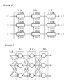
- Figure 5 shows the network in which the output of a plural number of neurons is integrated with the one neuron in the second layer. It also shows the connection of neural devices corresponding to Figure 4.
- each neural device COM2 In the first layer, the output of each neural device COM2 is input to other devices COM1 in order to integrate all the input data in each neuron. In the second layer, the data of neural device COM4 is sequentially transmitted to COM3 in order to integrated the output of the first layer, and finally it is integrated in the last neural device (the neural device at the top).
- Figure 7 shows a network for sequentially enlarging the number of the input data.
- Figure 6 shows the connection of neural devices corresponding to the network in Figure 7.
- each neural device COM2 In each layer, the output of each neural device COM2 is input to other neural devices COM1 because all the input data is necessary to be integrated in each neuron. OP of the neural device in each layer is input to the corresponding neuron in the following layer.
- each neural device is structured by IC or IC module, high speed processing and effective simulation can be performed.
- the wiring is easy because the connection among neural devices is very simple.
- the neural device comprises an input data output port for outputting at least a part of input data, an input data input port independent of an input port for inputting at least a part of input data, a summation input port for inputting data in addition to the summation of weighted input data, and a summation output port for outputting the summation. It realized to integrate, to divide, to use commonly input data, and to integrate and use commonly the summation. Therefore, it is possible to realize a network structure in more free way by hardware.
- C shows a computational means
- IP shows an input port
- OP shows an output port
- SP shows a converter which converts serial data into parallel data and parallel data into serial data
- COMP1 shows a communication port (input data input port)
- COMP2 shows a communication port (input data output port)
- COMP3 shows a communication port (summed value input port)
- COM4 shows a communication port (summed value output port).
Landscapes
- Engineering & Computer Science (AREA)
- Physics & Mathematics (AREA)
- Health & Medical Sciences (AREA)
- Life Sciences & Earth Sciences (AREA)
- Biomedical Technology (AREA)
- Biophysics (AREA)
- Theoretical Computer Science (AREA)
- Evolutionary Computation (AREA)
- General Engineering & Computer Science (AREA)
- Data Mining & Analysis (AREA)
- Artificial Intelligence (AREA)
- General Health & Medical Sciences (AREA)
- Molecular Biology (AREA)
- Computing Systems (AREA)
- Computational Linguistics (AREA)
- General Physics & Mathematics (AREA)
- Mathematical Physics (AREA)
- Software Systems (AREA)
- Neurology (AREA)
- Image Analysis (AREA)
- Design And Manufacture Of Integrated Circuits (AREA)
- Data Exchanges In Wide-Area Networks (AREA)
Applications Claiming Priority (2)
| Application Number | Priority Date | Filing Date | Title |
|---|---|---|---|
| JP3217955A JPH0567060A (ja) | 1991-08-02 | 1991-08-02 | ニユーロデバイス |
| JP217955/91 | 1991-08-02 |
Publications (3)
| Publication Number | Publication Date |
|---|---|
| EP0525543A2 true EP0525543A2 (fr) | 1993-02-03 |
| EP0525543A3 EP0525543A3 (en) | 1994-07-13 |
| EP0525543B1 EP0525543B1 (fr) | 1999-01-13 |
Family
ID=16712340
Family Applications (1)
| Application Number | Title | Priority Date | Filing Date |
|---|---|---|---|
| EP92112237A Expired - Lifetime EP0525543B1 (fr) | 1991-08-02 | 1992-07-17 | Dispositif neuronal du traitement de données |
Country Status (3)
| Country | Link |
|---|---|
| EP (1) | EP0525543B1 (fr) |
| JP (1) | JPH0567060A (fr) |
| DE (1) | DE69228150T2 (fr) |
Cited By (2)
| Publication number | Priority date | Publication date | Assignee | Title |
|---|---|---|---|---|
| US10387298B2 (en) | 2017-04-04 | 2019-08-20 | Hailo Technologies Ltd | Artificial neural network incorporating emphasis and focus techniques |
| KR20220147732A (ko) * | 2014-12-19 | 2022-11-03 | 인텔 코포레이션 | 인공 신경망에서의 분산 및 협력 계산을 위한 방법 및 장치 |
Families Citing this family (12)
| Publication number | Priority date | Publication date | Assignee | Title |
|---|---|---|---|---|
| RU2553098C2 (ru) * | 2013-08-23 | 2015-06-10 | Федеральное государственное унитарное предприятие "Научно-производственное объединение автоматики имени академика Н.А. Семихатова" | Нейровычислитель |
| JP6747305B2 (ja) * | 2017-01-17 | 2020-08-26 | 株式会社デンソー | データ処理装置及びニューラルネットワークシステム |
| US11238334B2 (en) | 2017-04-04 | 2022-02-01 | Hailo Technologies Ltd. | System and method of input alignment for efficient vector operations in an artificial neural network |
| US11551028B2 (en) | 2017-04-04 | 2023-01-10 | Hailo Technologies Ltd. | Structured weight based sparsity in an artificial neural network |
| US12430543B2 (en) | 2017-04-04 | 2025-09-30 | Hailo Technologies Ltd. | Structured sparsity guided training in an artificial neural network |
| US11544545B2 (en) | 2017-04-04 | 2023-01-03 | Hailo Technologies Ltd. | Structured activation based sparsity in an artificial neural network |
| US11615297B2 (en) | 2017-04-04 | 2023-03-28 | Hailo Technologies Ltd. | Structured weight based sparsity in an artificial neural network compiler |
| US12248367B2 (en) | 2020-09-29 | 2025-03-11 | Hailo Technologies Ltd. | Software defined redundant allocation safety mechanism in an artificial neural network processor |
| US11237894B1 (en) | 2020-09-29 | 2022-02-01 | Hailo Technologies Ltd. | Layer control unit instruction addressing safety mechanism in an artificial neural network processor |
| US11811421B2 (en) | 2020-09-29 | 2023-11-07 | Hailo Technologies Ltd. | Weights safety mechanism in an artificial neural network processor |
| US11263077B1 (en) | 2020-09-29 | 2022-03-01 | Hailo Technologies Ltd. | Neural network intermediate results safety mechanism in an artificial neural network processor |
| US11221929B1 (en) | 2020-09-29 | 2022-01-11 | Hailo Technologies Ltd. | Data stream fault detection mechanism in an artificial neural network processor |
Family Cites Families (1)
| Publication number | Priority date | Publication date | Assignee | Title |
|---|---|---|---|---|
| US4858177A (en) * | 1987-03-27 | 1989-08-15 | Smith Harry F | Minimal connectivity parallel data processing system |
-
1991
- 1991-08-02 JP JP3217955A patent/JPH0567060A/ja active Pending
-
1992
- 1992-07-17 EP EP92112237A patent/EP0525543B1/fr not_active Expired - Lifetime
- 1992-07-17 DE DE69228150T patent/DE69228150T2/de not_active Expired - Fee Related
Cited By (3)
| Publication number | Priority date | Publication date | Assignee | Title |
|---|---|---|---|---|
| KR20220147732A (ko) * | 2014-12-19 | 2022-11-03 | 인텔 코포레이션 | 인공 신경망에서의 분산 및 협력 계산을 위한 방법 및 장치 |
| US12032653B2 (en) | 2014-12-19 | 2024-07-09 | Intel Corporation | Method and apparatus for distributed and cooperative computation in artificial neural networks |
| US10387298B2 (en) | 2017-04-04 | 2019-08-20 | Hailo Technologies Ltd | Artificial neural network incorporating emphasis and focus techniques |
Also Published As
| Publication number | Publication date |
|---|---|
| JPH0567060A (ja) | 1993-03-19 |
| EP0525543B1 (fr) | 1999-01-13 |
| EP0525543A3 (en) | 1994-07-13 |
| DE69228150D1 (de) | 1999-02-25 |
| DE69228150T2 (de) | 1999-05-20 |
Similar Documents
| Publication | Publication Date | Title |
|---|---|---|
| EP0525543A2 (fr) | Dispositif neuronal | |
| US5089983A (en) | Charge domain vector-matrix product processing system | |
| US5799134A (en) | One dimensional systolic array architecture for neural network | |
| JPH07262158A (ja) | 時系列学習神経回路素子およびそれを用いた時系列学習神経回路 | |
| EP0459222A2 (fr) | Réseau neuronal | |
| KR930018384A (ko) | 정보처리장치 및 정보처리시스템 | |
| KR970062893A (ko) | 데이타 처리 장치 및 데이타 처리 방법 | |
| IE56104B1 (en) | Discrete cosine transform calculation processor | |
| US4454590A (en) | Programmable signal processing device | |
| US4546445A (en) | Systolic computational array | |
| GB2236608A (en) | Digital neural networks | |
| Ortigosa et al. | FPGA implementation of multi-layer perceptrons for speech recognition | |
| KR0175974B1 (ko) | 파이프라인 구조에 근거한 곱셈/나눗셈 공유 처리기 구조 | |
| US5148384A (en) | Signal processing integrated circuit | |
| GB2206428A (en) | Computer | |
| Schoenauer et al. | Simulation of a digital neuro-chip for spiking neural networks | |
| Tang et al. | Hardware implementations of multi-layer feedforward neural networks and error backpropagation using 8-bit PIC microcontrollers | |
| Bermak et al. | VLSI implementation of a neural network classifier based on the saturating linear activation function | |
| Magoulas et al. | A new method in neural network supervised training with imprecision | |
| RU2115161C1 (ru) | Вычислитель с перепрограммируемой архитектурой | |
| US5714901A (en) | Hysteretic coupling system | |
| SU1401457A1 (ru) | Логарифмический преобразователь | |
| Ortigosa et al. | FPGA implementation of a perceptron-like neural network for embedded applications | |
| SU1420605A1 (ru) | Аналого-цифрова вычислительна система | |
| Eppler et al. | High speed neural network chip for trigger purposes in high energy physics |
Legal Events
| Date | Code | Title | Description |
|---|---|---|---|
| PUAI | Public reference made under article 153(3) epc to a published international application that has entered the european phase |
Free format text: ORIGINAL CODE: 0009012 |
|
| AK | Designated contracting states |
Kind code of ref document: A2 Designated state(s): DE FR GB |
|
| RAP1 | Party data changed (applicant data changed or rights of an application transferred) |
Owner name: YOZAN INC. Owner name: EZEL ROBOT VISION INC. |
|
| RAP1 | Party data changed (applicant data changed or rights of an application transferred) |
Owner name: SHARP KABUSHIKI KAISHA Owner name: YOZAN INC. |
|
| PUAL | Search report despatched |
Free format text: ORIGINAL CODE: 0009013 |
|
| AK | Designated contracting states |
Kind code of ref document: A3 Designated state(s): DE FR GB |
|
| 17P | Request for examination filed |
Effective date: 19940629 |
|
| 17Q | First examination report despatched |
Effective date: 19970107 |
|
| GRAG | Despatch of communication of intention to grant |
Free format text: ORIGINAL CODE: EPIDOS AGRA |
|
| GRAG | Despatch of communication of intention to grant |
Free format text: ORIGINAL CODE: EPIDOS AGRA |
|
| GRAG | Despatch of communication of intention to grant |
Free format text: ORIGINAL CODE: EPIDOS AGRA |
|
| GRAH | Despatch of communication of intention to grant a patent |
Free format text: ORIGINAL CODE: EPIDOS IGRA |
|
| GRAH | Despatch of communication of intention to grant a patent |
Free format text: ORIGINAL CODE: EPIDOS IGRA |
|
| GRAA | (expected) grant |
Free format text: ORIGINAL CODE: 0009210 |
|
| AK | Designated contracting states |
Kind code of ref document: B1 Designated state(s): DE FR GB |
|
| PG25 | Lapsed in a contracting state [announced via postgrant information from national office to epo] |
Ref country code: FR Free format text: THE PATENT HAS BEEN ANNULLED BY A DECISION OF A NATIONAL AUTHORITY Effective date: 19990113 |
|
| REF | Corresponds to: |
Ref document number: 69228150 Country of ref document: DE Date of ref document: 19990225 |
|
| ET | Fr: translation filed | ||
| PG25 | Lapsed in a contracting state [announced via postgrant information from national office to epo] |
Ref country code: GB Free format text: LAPSE BECAUSE OF NON-PAYMENT OF DUE FEES Effective date: 19990717 |
|
| PLBE | No opposition filed within time limit |
Free format text: ORIGINAL CODE: 0009261 |
|
| STAA | Information on the status of an ep patent application or granted ep patent |
Free format text: STATUS: NO OPPOSITION FILED WITHIN TIME LIMIT |
|
| 26N | No opposition filed | ||
| GBPC | Gb: european patent ceased through non-payment of renewal fee |
Effective date: 19990717 |
|
| PG25 | Lapsed in a contracting state [announced via postgrant information from national office to epo] |
Ref country code: DE Free format text: LAPSE BECAUSE OF NON-PAYMENT OF DUE FEES Effective date: 20000503 |
|
| REG | Reference to a national code |
Ref country code: FR Ref legal event code: ST |