EP0526657A1 - Dispositif de deposition en phase vapeur par procede chimique du type a plasma hyperfrequence et procede de synthese du diamant au moyen d'un tel dispositif - Google Patents
Dispositif de deposition en phase vapeur par procede chimique du type a plasma hyperfrequence et procede de synthese du diamant au moyen d'un tel dispositif Download PDFInfo
- Publication number
- EP0526657A1 EP0526657A1 EP92905297A EP92905297A EP0526657A1 EP 0526657 A1 EP0526657 A1 EP 0526657A1 EP 92905297 A EP92905297 A EP 92905297A EP 92905297 A EP92905297 A EP 92905297A EP 0526657 A1 EP0526657 A1 EP 0526657A1
- Authority
- EP
- European Patent Office
- Prior art keywords
- microwave
- plunger
- waveguide
- plasma
- reaction tube
- Prior art date
- Legal status (The legal status is an assumption and is not a legal conclusion. Google has not performed a legal analysis and makes no representation as to the accuracy of the status listed.)
- Withdrawn
Links
- 239000010432 diamond Substances 0.000 title claims abstract description 32
- 229910003460 diamond Inorganic materials 0.000 title claims abstract description 31
- 238000000034 method Methods 0.000 title claims abstract description 11
- 230000002194 synthesizing effect Effects 0.000 title claims abstract description 9
- 238000006243 chemical reaction Methods 0.000 claims description 62
- 238000005229 chemical vapour deposition Methods 0.000 claims description 9
- OKTJSMMVPCPJKN-UHFFFAOYSA-N Carbon Chemical compound [C] OKTJSMMVPCPJKN-UHFFFAOYSA-N 0.000 claims description 5
- 229910052799 carbon Inorganic materials 0.000 claims description 5
- 230000000644 propagated effect Effects 0.000 claims description 3
- 238000005268 plasma chemical vapour deposition Methods 0.000 abstract description 24
- 239000000758 substrate Substances 0.000 description 24
- 239000010408 film Substances 0.000 description 20
- 239000007789 gas Substances 0.000 description 15
- 239000000463 material Substances 0.000 description 11
- 239000010409 thin film Substances 0.000 description 8
- -1 olefin hydrocarbon Chemical class 0.000 description 6
- 239000004215 Carbon black (E152) Substances 0.000 description 5
- 239000000498 cooling water Substances 0.000 description 5
- 238000005520 cutting process Methods 0.000 description 5
- 229930195733 hydrocarbon Natural products 0.000 description 5
- 238000001816 cooling Methods 0.000 description 4
- UHOVQNZJYSORNB-UHFFFAOYSA-N Benzene Chemical compound C1=CC=CC=C1 UHOVQNZJYSORNB-UHFFFAOYSA-N 0.000 description 3
- LFQSCWFLJHTTHZ-UHFFFAOYSA-N Ethanol Chemical compound CCO LFQSCWFLJHTTHZ-UHFFFAOYSA-N 0.000 description 3
- OKKJLVBELUTLKV-UHFFFAOYSA-N Methanol Chemical compound OC OKKJLVBELUTLKV-UHFFFAOYSA-N 0.000 description 3
- YXFVVABEGXRONW-UHFFFAOYSA-N Toluene Chemical compound CC1=CC=CC=C1 YXFVVABEGXRONW-UHFFFAOYSA-N 0.000 description 3
- ZMANZCXQSJIPKH-UHFFFAOYSA-N Triethylamine Chemical compound CCN(CC)CC ZMANZCXQSJIPKH-UHFFFAOYSA-N 0.000 description 3
- XLYOFNOQVPJJNP-UHFFFAOYSA-N water Substances O XLYOFNOQVPJJNP-UHFFFAOYSA-N 0.000 description 3
- CSCPPACGZOOCGX-UHFFFAOYSA-N Acetone Chemical compound CC(C)=O CSCPPACGZOOCGX-UHFFFAOYSA-N 0.000 description 2
- ATUOYWHBWRKTHZ-UHFFFAOYSA-N Propane Chemical compound CCC ATUOYWHBWRKTHZ-UHFFFAOYSA-N 0.000 description 2
- XUIMIQQOPSSXEZ-UHFFFAOYSA-N Silicon Chemical compound [Si] XUIMIQQOPSSXEZ-UHFFFAOYSA-N 0.000 description 2
- 239000006227 byproduct Substances 0.000 description 2
- 238000009826 distribution Methods 0.000 description 2
- 238000004519 manufacturing process Methods 0.000 description 2
- VNWKTOKETHGBQD-UHFFFAOYSA-N methane Chemical compound C VNWKTOKETHGBQD-UHFFFAOYSA-N 0.000 description 2
- 239000000203 mixture Substances 0.000 description 2
- FDPIMTJIUBPUKL-UHFFFAOYSA-N pentan-3-one Chemical compound CCC(=O)CC FDPIMTJIUBPUKL-UHFFFAOYSA-N 0.000 description 2
- 239000010453 quartz Substances 0.000 description 2
- 229910052710 silicon Inorganic materials 0.000 description 2
- 239000010703 silicon Substances 0.000 description 2
- VYPSYNLAJGMNEJ-UHFFFAOYSA-N silicon dioxide Inorganic materials O=[Si]=O VYPSYNLAJGMNEJ-UHFFFAOYSA-N 0.000 description 2
- GETQZCLCWQTVFV-UHFFFAOYSA-N trimethylamine Chemical compound CN(C)C GETQZCLCWQTVFV-UHFFFAOYSA-N 0.000 description 2
- UGFAIRIUMAVXCW-UHFFFAOYSA-N Carbon monoxide Chemical compound [O+]#[C-] UGFAIRIUMAVXCW-UHFFFAOYSA-N 0.000 description 1
- LVZWSLJZHVFIQJ-UHFFFAOYSA-N Cyclopropane Chemical compound C1CC1 LVZWSLJZHVFIQJ-UHFFFAOYSA-N 0.000 description 1
- MYMOFIZGZYHOMD-UHFFFAOYSA-N Dioxygen Chemical compound O=O MYMOFIZGZYHOMD-UHFFFAOYSA-N 0.000 description 1
- OTMSDBZUPAUEDD-UHFFFAOYSA-N Ethane Chemical compound CC OTMSDBZUPAUEDD-UHFFFAOYSA-N 0.000 description 1
- HSFWRNGVRCDJHI-UHFFFAOYSA-N alpha-acetylene Natural products C#C HSFWRNGVRCDJHI-UHFFFAOYSA-N 0.000 description 1
- 229910052782 aluminium Inorganic materials 0.000 description 1
- XAGFODPZIPBFFR-UHFFFAOYSA-N aluminium Chemical compound [Al] XAGFODPZIPBFFR-UHFFFAOYSA-N 0.000 description 1
- 150000001412 amines Chemical class 0.000 description 1
- 150000004945 aromatic hydrocarbons Chemical class 0.000 description 1
- 230000005540 biological transmission Effects 0.000 description 1
- 230000015572 biosynthetic process Effects 0.000 description 1
- 239000001273 butane Substances 0.000 description 1
- 229910002091 carbon monoxide Inorganic materials 0.000 description 1
- 230000000052 comparative effect Effects 0.000 description 1
- 229910001882 dioxygen Inorganic materials 0.000 description 1
- 238000007599 discharging Methods 0.000 description 1
- 238000006073 displacement reaction Methods 0.000 description 1
- 230000005684 electric field Effects 0.000 description 1
- 238000010438 heat treatment Methods 0.000 description 1
- 150000002430 hydrocarbons Chemical class 0.000 description 1
- 230000001788 irregular Effects 0.000 description 1
- 150000002576 ketones Chemical class 0.000 description 1
- 230000001050 lubricating effect Effects 0.000 description 1
- 229910052751 metal Inorganic materials 0.000 description 1
- 239000002184 metal Substances 0.000 description 1
- IJDNQMDRQITEOD-UHFFFAOYSA-N n-butane Chemical compound CCCC IJDNQMDRQITEOD-UHFFFAOYSA-N 0.000 description 1
- OFBQJSOFQDEBGM-UHFFFAOYSA-N n-pentane Natural products CCCCC OFBQJSOFQDEBGM-UHFFFAOYSA-N 0.000 description 1
- JRZJOMJEPLMPRA-UHFFFAOYSA-N olefin Natural products CCCCCCCC=C JRZJOMJEPLMPRA-UHFFFAOYSA-N 0.000 description 1
- 230000003287 optical effect Effects 0.000 description 1
- 239000012188 paraffin wax Substances 0.000 description 1
- 239000000047 product Substances 0.000 description 1
- 239000001294 propane Substances 0.000 description 1
- 239000004065 semiconductor Substances 0.000 description 1
- 238000003786 synthesis reaction Methods 0.000 description 1
Images


Classifications
-
- H—ELECTRICITY
- H01—ELECTRIC ELEMENTS
- H01J—ELECTRIC DISCHARGE TUBES OR DISCHARGE LAMPS
- H01J37/00—Discharge tubes with provision for introducing objects or material to be exposed to the discharge, e.g. for the purpose of examination or processing thereof
- H01J37/32—Gas-filled discharge tubes
- H01J37/32009—Arrangements for generation of plasma specially adapted for examination or treatment of objects, e.g. plasma sources
- H01J37/32192—Microwave generated discharge
- H01J37/32211—Means for coupling power to the plasma
- H01J37/32247—Resonators
- H01J37/32256—Tuning means
-
- C—CHEMISTRY; METALLURGY
- C23—COATING METALLIC MATERIAL; COATING MATERIAL WITH METALLIC MATERIAL; CHEMICAL SURFACE TREATMENT; DIFFUSION TREATMENT OF METALLIC MATERIAL; COATING BY VACUUM EVAPORATION, BY SPUTTERING, BY ION IMPLANTATION OR BY CHEMICAL VAPOUR DEPOSITION, IN GENERAL; INHIBITING CORROSION OF METALLIC MATERIAL OR INCRUSTATION IN GENERAL
- C23C—COATING METALLIC MATERIAL; COATING MATERIAL WITH METALLIC MATERIAL; SURFACE TREATMENT OF METALLIC MATERIAL BY DIFFUSION INTO THE SURFACE, BY CHEMICAL CONVERSION OR SUBSTITUTION; COATING BY VACUUM EVAPORATION, BY SPUTTERING, BY ION IMPLANTATION OR BY CHEMICAL VAPOUR DEPOSITION, IN GENERAL
- C23C16/00—Chemical coating by decomposition of gaseous compounds, without leaving reaction products of surface material in the coating, i.e. chemical vapour deposition [CVD] processes
- C23C16/22—Chemical coating by decomposition of gaseous compounds, without leaving reaction products of surface material in the coating, i.e. chemical vapour deposition [CVD] processes characterised by the deposition of inorganic material, other than metallic material
- C23C16/26—Deposition of carbon only
- C23C16/27—Diamond only
-
- C—CHEMISTRY; METALLURGY
- C23—COATING METALLIC MATERIAL; COATING MATERIAL WITH METALLIC MATERIAL; CHEMICAL SURFACE TREATMENT; DIFFUSION TREATMENT OF METALLIC MATERIAL; COATING BY VACUUM EVAPORATION, BY SPUTTERING, BY ION IMPLANTATION OR BY CHEMICAL VAPOUR DEPOSITION, IN GENERAL; INHIBITING CORROSION OF METALLIC MATERIAL OR INCRUSTATION IN GENERAL
- C23C—COATING METALLIC MATERIAL; COATING MATERIAL WITH METALLIC MATERIAL; SURFACE TREATMENT OF METALLIC MATERIAL BY DIFFUSION INTO THE SURFACE, BY CHEMICAL CONVERSION OR SUBSTITUTION; COATING BY VACUUM EVAPORATION, BY SPUTTERING, BY ION IMPLANTATION OR BY CHEMICAL VAPOUR DEPOSITION, IN GENERAL
- C23C16/00—Chemical coating by decomposition of gaseous compounds, without leaving reaction products of surface material in the coating, i.e. chemical vapour deposition [CVD] processes
- C23C16/44—Chemical coating by decomposition of gaseous compounds, without leaving reaction products of surface material in the coating, i.e. chemical vapour deposition [CVD] processes characterised by the method of coating
- C23C16/50—Chemical coating by decomposition of gaseous compounds, without leaving reaction products of surface material in the coating, i.e. chemical vapour deposition [CVD] processes characterised by the method of coating using electric discharges
- C23C16/511—Chemical coating by decomposition of gaseous compounds, without leaving reaction products of surface material in the coating, i.e. chemical vapour deposition [CVD] processes characterised by the method of coating using electric discharges using microwave discharges
-
- H—ELECTRICITY
- H01—ELECTRIC ELEMENTS
- H01J—ELECTRIC DISCHARGE TUBES OR DISCHARGE LAMPS
- H01J37/00—Discharge tubes with provision for introducing objects or material to be exposed to the discharge, e.g. for the purpose of examination or processing thereof
- H01J37/32—Gas-filled discharge tubes
- H01J37/32009—Arrangements for generation of plasma specially adapted for examination or treatment of objects, e.g. plasma sources
- H01J37/32192—Microwave generated discharge
Definitions
- the present invention relates to a microwave plasma chemical vapor deposition (CVD) apparatus which is capable of two-dimensionally adjusting the position of a plasma in a reaction tube, and a method of synthesizing a diamond film of uniform quality and thickness on a substrate with the microwave plasma CVD apparatus.
- CVD microwave plasma chemical vapor deposition
- the microwave plasma CVD process employs a microwave to excite and decompose a material gas to generate a plasma which forms a thin film on a substrate or a base.
- the microwave plasma CVD process is finding use in a wide range of applications from the fabrication of semiconductors to the synthesis of thin films of diamond.
- the microwave plasma CVD process is highly practical as it can achieve desired film qualities, film thicknesses, and film yields with high reproducibility.
- the microwave plasma CVD apparatus includes a microwave waveguide 2a having an end 2b and an E plane which is perpendicular to an electric vector, and a cylindrical reaction tube 6 of quartz extending through the waveguide 2a perpendicularly to the E plane at a position adjacent to the end 2b of the waveguide 2a.
- a shorting plunger 5 is mounted in the end 2b of the waveguide 2a.
- the shorting plunger 5 serves as a short-circuiting device for fully reflecting a microwave which has traveled in the waveguide 2a.
- a plasma generated in the reaction tube 6 is moved several cm only in the direction of travel of the microwave, thereby finely adjusting the position where the plasma is generated.
- the microwave plasma CVD apparatus is usually adjusted in advance to position of the center of the plasma at the central axis of the reaction tube 6.
- the position where the plasma is generated can be moved one-dimensionally in the direction of travel of the microwave.
- reaction tube 6 of quarts Since the reaction tube 6 of quarts is transparent, it does not inherently absorb or reflect the microwave. However, if any by-product is deposited on the inner wall surface of the reaction tube 6 during a reaction process, then the by-product deposit absorbs or reflects the microwave.
- any changes in the cross-sectional area of the waveguide 2a or the presence of electric charges or currents in the waveguide wall may interrupt electric and magnetic fields, causing the microwave to spread in perpendicular and oblique directions as well as to travel straight.
- the plasma and the base on which the thin film is to be formed have an ununiform distribution of temperatures.
- the quality of the diamond film, the rate at which the diamond film is synthesized, and the thickness of the diamond film become irregular.
- the synthesized diamond film is used as the film on a diamond-coated tool, e.g., a cutting tool, the cutting performance and the tool life may vary due to the different thicknesses of the diamond film at the respective corners of the cutting tip of the tool. Therefore, the tool cannot be used for stably cutting work-pieces.
- Another object of the present invention is to provide a method of synthesizing a diamond film of uniform quality and thickness on a substrate with the above microwave plasma CVD apparatus.
- the inventors has conducted intensive research and found out that it is possible to move a plasma generated in a reaction tube in a direction perpendicular to the direction of travel of a microwave, with a shorting plunger which can make fine adjustment of the diameter of the reaction tube.
- a microwave plasma chemical vapor deposition apparatus comprising a microwave oscillator, a microwave waveguide, a first plunger mounted in an end of the microwave waveguide, and a reaction tube extending through the microwave waveguide perpendicularly to an E plane thereof adjacent to the end of the microwave waveguide, the microwave waveguide and the reaction tube jointly defining a reaction region at an intersection thereof, wherein the improvement comprises a second plunger disposed on an H plane of the microwave guide adjacent to the end thereof, the second plunger extending perpendicularly to the microwave waveguide and the reaction tube and facing the reaction region.
- a method of synthesizing diamond using the above microwave plasma chemical vapor deposition apparatus comprising the steps of exciting a carbon source gas and forming a diamond film on a base.
- the position of the plasma in the reaction tube is two-dimensionally adjusted to form a diamond or diamond-like thin film having a uniform quality and a uniform thickness on a substrate or base.
- a diamond or diamond-like thin film will hereinafter be referred to as diamond or a diamond film.
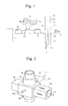
- a microwave plasma CVD apparatus generally comprises a microwave oscillator 1, a microwave waveguide 2a, a cylindrical reaction tube 6, and a plunger 5.
- the microwave oscillator 1 generates a microwave of a predetermined frequency, e.g., 2.45 GHz.
- the generated microwave may be directly introduced into the reaction tube 6, or may be introduced into the reaction tube 6 after it has been modulated into a pulse wave.
- the microwave waveguide 2a is in the form of a hollow transmission device of metal in which the microwave generated by the microwave oscillator 1 is propagated.
- the microwave waveguide 2a usually comprises a rectangular waveguide having a rectangular cross-sectional shape.
- a power monitor 3 is connected to the microwave waveguide 2a.
- the microwave waveguide 2a has two spaced three-stub tuners (matching devices) 4.
- the power monitor 3 measures output intensities of supplied and reflected waves, and regulates the three-stub tuners 4 so that the reflected wave will be minimized.
- the power monitor 3 comprises a power monitor unit 3a for measuring the output intensity of the supplied wave, and a power monitor unit 3b for measuring the output intensity of the reflected wave.
- a first plunger 5 which is the same as the known shorting plunger, is mounted in an end 2b of the microwave waveguide 2a.
- the plunger 5 serves as a short-circuiting device for fully reflecting a microwave which has traveled in the waveguide 2a.
- the reaction tube 6 extends vertically through the microwave waveguide 2a perpendicularly to a E plane of the microwave waveguide 2a at a position adjacent to the end 2b thereof.
- a space region in the reaction tube 6 where the reaction tube 6 and the microwave waveguide 2a intersect with each other serves as a reaction region 7 in which a plasma is generated for reaction.
- the reaction tube 6 is usually made of a material such as quartz which allows the microwave to pass therethrough without loss and which is chemically stable.
- the reaction tube 6 extends perpendicular to the upper surface (lying in the E plane which contains a longer side of the rectangular cross-sectional shape of the microwave waveguide 6) of the microwave waveguide 6 because a leakage of the microwave in a direction perpendicular to the upper surface of the microwave waveguide 6 is greater than a leakage of the microwave in a direction perpendicular to a side surface (lying in an H plane which contains a shorter side of the rectangular cross-sectional shape of the microwave waveguide 6) of the microwave waveguide 6.
- the microwave plasma CVD apparatus also has a plunger assembly 8 mounted on a side surface (H plane) of the microwave waveguide 2a adjacent to the end 2b thereof.
- the plunger assembly 8 lies perpendicularly to both the microwave waveguide 2a and the reaction tube 6, and faces the reaction region 7.
- the plunger assembly 8 comprises a second plunger (side shorting plunger) 9.
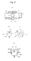
- Each of the first and second plungers 5, 9 may comprise a fully reflecting plunger 10 as shown in FIG. 3(a).
- the second plunger 9 may alternatively be in the form of a plate 11 as shown in FIG. 3(b) or a pin 12 as shown in FIG. 3(c).
- the second plunger 9 should preferably be of the fully reflecting type as shown in FIG. 3(a) in view of the generation of heat owing to a loss of microwave.
- An opening in the microwave waveguide 2a which leads to the second plunger 9 should preferably have a length equal to half of the wavelength of the microwave in the direction in which the microwave travels.
- a substrate holder 13 is disposed in the reaction region 7 in the reaction tube 6, and a substrate 14 is placed on the substrate holder 13.
- the substrate holder 13 is associated with a heating means or a cooling means for adjusting the temperature of the substrate 14.
- a base holder 13 suitable for supporting and fixing such a base is prepared.
- a material gas supply pipe 15 is connected to an upper portion of the reaction tube 6 for supplying a material gas (including a plasma gas) into the reaction tube 6.
- An evacuating pump 16 is connected to a lower portion of the reaction tube 6 for evacuating the reaction tube 6 to a certain vacuum.
- a double-walled water cooling jacket 17 is disposed around the reaction tube 6 in the vicinity of the reaction region 7 for passing cooling water therethrough to cool the reaction tube 6 to prevent the reaction tube 6 and its surrounding area from being excessively heated.
- the water cooling jacket 17 has a cooling water inlet 18 for introducing the cooling water and a cooling water outlet 19 for discharging the cooling water.
- the portion of the water cooling jacket 17 which intersects with the microwave waveguide 2a has a window for passage of the microwave therethrough.
- An observation window 20 is provided for the operator to observe the condition of the plasma and the vertical position of the base in the reaction region 7.
- the observation window 20 normally comprises a pipe having a length of 40 mm and a diameter of 10 mm for preventing the microwave from leaking out of the reaction region 7.
- a close observation of the energized condition of the plasma, particularly a positional displacement of the plasma in the direction of the second plunger 9, is made through an observation window on the upper portion of the reaction tube 6.
- the second plunger may be provided in the observation window 20. More specifically, a simple plunger 22 shown in FIGS. 4(b) and 4(c) is disposed in an observation hole 21 of the observation window 20 shown in FIG. 4(a) in covering relationship to the observation hole 21 as shown in FIG. 4-(d). Therefore, the observation window 20 and the plunger 22 are combined with each other in a simple arrangement.
- the plunger 22 comprises a plate 23 and a support 24, both made of aluminum.
- the reaction tube 6 is evacuated by the evacuating pump 16, and then a material gas (including a plasma gas) is supplied into the reaction tube 6 through the material gas supply pipe 15.
- the material gas for use in synthesizing diamond comprises a mixture of a carbon source gas and an oxygen gas.
- the carbon source gas may be a paraffin hydrocarbon such as methane, ethane, propane, butane, or the like, an olefin hydrocarbon such as ethylene, propylene, butylene, or the like, an acetylene hydrocarbon, a diolefin hydrocarbon, an alicyclic hydrocarbon such as cyclopropane, cyclobuthane, or the like, an aromatic hydrocarbon such as benzene, toluene, or the like, a ketone such as acetone, diethyl ketone, or the like, an alcohol such as methanol, ethanol, or the like, an amine such as trimethylamine, triethylamine, or the like, a carbon gas, or carbon monoxide, or a mixture thereof.
- a paraffin hydrocarbon such as methane, ethane, propane, butane, or the like
- an olefin hydrocarbon such as ethylene, propylene, butylene, or the like
- a microwave is generated by the microwave oscillator 1, and introduced through the microwave waveguide 2a into the reaction region 7 in the reaction tube 6.
- the material gas is excited by the microwave and decomposed to generate a plasma around the substrate 14.
- a diamond film is uniformly deposited by way of vapor growth on the substrate 14 because of the plasma.
- the reaction region 7 may be kept under a pressure ranging from 10- 3 to 10 3 Torr, preferably from 1 to 800 Torr.
- the temperature of the surface of the substrate 14 may be in the range of from 300 to 1000°C, preferably from 450 to 950 ° C.
- the reaction may continue for such a period of time that the deposited diamond film has a thickness of 1 /1.m or more, preferably in the range of from 2 to 10 /1.m.
- the operator observes the positional relationship between the substrate 14 and the plasma through the observation window on the upper portion of the reaction tube 6. If there is any positional deviation between the substrate 14 and the plasma, then the operator moves the first plunger 5 and/or the second plunger 9 to adjust the position of the plasma.
- the position of the plasma in the direction of travel of the plasma can be adjusted with the first plunger 5, and the position of the plasma in the direction perpendicular to the direction of travel of the plasma can be adjusted with the second plunger 9.
- the positional movement of the plasma is basically related to the movement of the first and second plungers 5, 9.
- the microwave reflected thereby is brought out of phase, causing the plasma to move to the left or right.
- the second plunger 9 Upon movement of the second plunger 9 in a forward (downward) direction or a rearward (upward) direction in FIG. 5, the amplitude of the microwave varies out of its center, and the plasma moves forwardly or rearwardly.
- the dimension a of a space defined between the first plunger 5 and the reaction tube 6 is such that the reflecting surface of the first plunger 5 is spaced from the center of the reaction tube 6 by a distance which is an integral multiple of half of the wavelength of the microwave, preferably 1 to 4 times half of the wavelength of the microwave.
- the dimension a should preferably be adjustable in a range of ⁇ 1 cm.
- the dimension b of a space defined between the second plunger 9 and the reaction tube 6 is such that the reflecting surface of the second plunger 9 is aligned with an inner wall surface of the reaction tube 6.
- the dimension b should preferably be adjustable in a range of ⁇ 1 cm.
- the dimension a was 7.5 cm, and the dimension b was 0 cm. Then, the first and second plungers 5, 9 were actuated while the position of the plasma was being observed through the observation window on the upper portion of the reaction tube 6. It was confirmed that the plasma was moved in the respective directions of the plungers for positional adjustment thereof.
Landscapes
- Chemical & Material Sciences (AREA)
- Engineering & Computer Science (AREA)
- Physics & Mathematics (AREA)
- Plasma & Fusion (AREA)
- General Chemical & Material Sciences (AREA)
- Analytical Chemistry (AREA)
- Chemical Kinetics & Catalysis (AREA)
- Materials Engineering (AREA)
- Mechanical Engineering (AREA)
- Metallurgy (AREA)
- Organic Chemistry (AREA)
- Inorganic Chemistry (AREA)
- Crystals, And After-Treatments Of Crystals (AREA)
- Chemical Vapour Deposition (AREA)
Abstract
L'invention se rapporte à un dispositif de déposition en phase vapeur par procédé chimique du type à plasma hyperfréquence, au moyen duquel on peut effectuer un réglage bidimensionnel de la position d'un plasma dans un tube réactif, ainsi qu'à un procédé permettant d'effectuer la synthèse de diamants au moyen de ce dispositif. A cet effet, un guide d'ondes (2a) est placé en connexion avec un oscillateur hyperfréquence (1). Un second plongeur (9) (section plongeur (8)) est disposé sur le côté H de la partie terminale (2b) du guide d'ondes (2a), à l'opposé d'une section réactive. En actionnant le plongeur (9), on parvient à déplacer le plasma également dans le sens perpendiculaire à la direction d'avance de l'onde hyperfréquence, et on peut procéder à un réglage bidimensionnel de la position du plasma. On peut alors obtenir des films de diamant de qualité et d'épaisseur uniformes.
Applications Claiming Priority (2)
| Application Number | Priority Date | Filing Date | Title |
|---|---|---|---|
| JP5407291 | 1991-02-26 | ||
| JP54072/91 | 1991-02-26 |
Publications (2)
| Publication Number | Publication Date |
|---|---|
| EP0526657A1 true EP0526657A1 (fr) | 1993-02-10 |
| EP0526657A4 EP0526657A4 (en) | 1995-12-13 |
Family
ID=12960417
Family Applications (1)
| Application Number | Title | Priority Date | Filing Date |
|---|---|---|---|
| EP92905297A Withdrawn EP0526657A4 (en) | 1991-02-26 | 1992-02-25 | Microwave plasma cvd device, and method for synthesizing diamond by device thereof |
Country Status (3)
| Country | Link |
|---|---|
| US (1) | US5292371A (fr) |
| EP (1) | EP0526657A4 (fr) |
| WO (1) | WO1992014861A1 (fr) |
Cited By (8)
| Publication number | Priority date | Publication date | Assignee | Title |
|---|---|---|---|---|
| EP0822572A1 (fr) * | 1995-04-07 | 1998-02-04 | Michigan State University | Méthode et appareil de traitement de surface par plasma |
| WO2012084658A1 (fr) * | 2010-12-23 | 2012-06-28 | Element Six Limited | Système de distribution de puissance hyperfréquence destiné à des réacteurs à plasma |
| WO2012084659A3 (fr) * | 2010-12-23 | 2012-08-23 | Element Six Limited | Réacteur à plasma hyperfréquence permettant de fabriquer un matériau en diamant synthétique |
| US8859058B2 (en) | 2010-12-23 | 2014-10-14 | Element Six Limited | Microwave plasma reactors and substrates for synthetic diamond manufacture |
| US9410242B2 (en) | 2010-12-23 | 2016-08-09 | Element Six Technologies Limited | Microwave plasma reactor for manufacturing synthetic diamond material |
| US9637838B2 (en) | 2010-12-23 | 2017-05-02 | Element Six Limited | Methods of manufacturing synthetic diamond material by microwave plasma enhanced chemical vapor deposition from a microwave generator and gas inlet(s) disposed opposite the growth surface area |
| US10403477B2 (en) | 2010-12-23 | 2019-09-03 | Element Six Technologies Limited | Microwave plasma reactor for manufacturing synthetic diamond material |
| US11371147B2 (en) | 2010-12-23 | 2022-06-28 | Element Six Technologies Limited | Microwave plasma reactor for manufacturing synthetic diamond material |
Families Citing this family (5)
| Publication number | Priority date | Publication date | Assignee | Title |
|---|---|---|---|---|
| EP0702393A3 (fr) * | 1994-09-16 | 1997-03-26 | Daihen Corp | Appareil de traitement par plasma pour introduire une onde micrométrique issue d'un guide d'onde rectangulaire, à travers une feute allongée dans la chambre à plasma |
| US6696662B2 (en) * | 2000-05-25 | 2004-02-24 | Advanced Energy Industries, Inc. | Methods and apparatus for plasma processing |
| JP5023420B2 (ja) * | 2001-07-19 | 2012-09-12 | 凸版印刷株式会社 | プラズマcvd装置 |
| WO2009096953A1 (fr) * | 2008-01-30 | 2009-08-06 | Applied Materials, Inc. | Guide d'ondes pour micro-ondes intégré avec transition d'impédance |
| US20250101577A1 (en) * | 2023-09-21 | 2025-03-27 | Board Of Trustees Of Michigan State University | Microwave Capillary Nanodiamond Reactor |
Family Cites Families (4)
| Publication number | Priority date | Publication date | Assignee | Title |
|---|---|---|---|---|
| JPS5211175A (en) * | 1975-07-18 | 1977-01-27 | Toshiba Corp | Activated gas reacting apparatus |
| JPS63166970A (ja) * | 1986-12-26 | 1988-07-11 | Seiko Instr & Electronics Ltd | 炭素膜の合成方法 |
| JPS6465279A (en) * | 1987-09-04 | 1989-03-10 | Seiko Instr & Electronics | Microwave plasma reaction apparatus |
| FR2647293B1 (fr) * | 1989-05-18 | 1996-06-28 | Defitech Sa | Reacteur a plasma perfectionne muni de moyens de couplage d'ondes electromagnetiques |
-
1992
- 1992-02-25 WO PCT/JP1992/000205 patent/WO1992014861A1/fr not_active Ceased
- 1992-02-25 EP EP92905297A patent/EP0526657A4/en not_active Withdrawn
- 1992-10-26 US US07/966,368 patent/US5292371A/en not_active Expired - Fee Related
Non-Patent Citations (2)
| Title |
|---|
| No further relevant documents disclosed * |
| See also references of WO9214861A1 * |
Cited By (16)
| Publication number | Priority date | Publication date | Assignee | Title |
|---|---|---|---|---|
| EP0822572A1 (fr) * | 1995-04-07 | 1998-02-04 | Michigan State University | Méthode et appareil de traitement de surface par plasma |
| WO2012084658A1 (fr) * | 2010-12-23 | 2012-06-28 | Element Six Limited | Système de distribution de puissance hyperfréquence destiné à des réacteurs à plasma |
| WO2012084659A3 (fr) * | 2010-12-23 | 2012-08-23 | Element Six Limited | Réacteur à plasma hyperfréquence permettant de fabriquer un matériau en diamant synthétique |
| CN103415647A (zh) * | 2010-12-23 | 2013-11-27 | 六号元素有限公司 | 用于等离子体反应器的微波功率传输系统 |
| US8859058B2 (en) | 2010-12-23 | 2014-10-14 | Element Six Limited | Microwave plasma reactors and substrates for synthetic diamond manufacture |
| KR101454568B1 (ko) * | 2010-12-23 | 2014-10-23 | 엘리멘트 식스 리미티드 | 합성 다이아몬드 제조용의 마이크로파 플라즈마 반응기 및 기재 |
| KR101454569B1 (ko) * | 2010-12-23 | 2014-10-23 | 엘리멘트 식스 리미티드 | 합성 다이아몬드 물질을 제조하기 위한 마이크로파 플라즈마 반응기 |
| US8955456B2 (en) | 2010-12-23 | 2015-02-17 | Element Six Limited | Microwave plasma reactor for manufacturing synthetic diamond material |
| CN103415647B (zh) * | 2010-12-23 | 2015-08-19 | 六号元素有限公司 | 用于等离子体反应器的微波功率传输系统 |
| US9142389B2 (en) | 2010-12-23 | 2015-09-22 | Element Six Technologies Limited | Microwave power delivery system for plasma reactors |
| US9410242B2 (en) | 2010-12-23 | 2016-08-09 | Element Six Technologies Limited | Microwave plasma reactor for manufacturing synthetic diamond material |
| US9637838B2 (en) | 2010-12-23 | 2017-05-02 | Element Six Limited | Methods of manufacturing synthetic diamond material by microwave plasma enhanced chemical vapor deposition from a microwave generator and gas inlet(s) disposed opposite the growth surface area |
| US9738970B2 (en) | 2010-12-23 | 2017-08-22 | Element Six Limited | Microwave plasma reactors and substrates for synthetic diamond manufacture |
| US10403477B2 (en) | 2010-12-23 | 2019-09-03 | Element Six Technologies Limited | Microwave plasma reactor for manufacturing synthetic diamond material |
| US11371147B2 (en) | 2010-12-23 | 2022-06-28 | Element Six Technologies Limited | Microwave plasma reactor for manufacturing synthetic diamond material |
| US11488805B2 (en) | 2010-12-23 | 2022-11-01 | Element Six Technologies Limited | Microwave plasma reactor for manufacturing synthetic diamond material |
Also Published As
| Publication number | Publication date |
|---|---|
| EP0526657A4 (en) | 1995-12-13 |
| US5292371A (en) | 1994-03-08 |
| WO1992014861A1 (fr) | 1992-09-03 |
Similar Documents
| Publication | Publication Date | Title |
|---|---|---|
| US5292371A (en) | Microwave plasma CVD apparatus comprising dual plungers for two-dimension plasma position adjustment | |
| US5188862A (en) | Microwave plasma generating apparatus and process for the preparation of diamond thin film utilizing same | |
| JP5364054B2 (ja) | 調整可能なマルチゾーンガス噴射システム | |
| EP1145277B1 (fr) | Systeme d'injection de gaz pour traitement au plasma | |
| CA2182247C (fr) | Appareil et methode pour le traitement d'un substrat par le biais du plasma dirige au-dessous de l'ouverture menant de la chambre vers l'emplacement du substrat | |
| US4869924A (en) | Method for synthesis of diamond and apparatus therefor | |
| US20080226840A1 (en) | Process for synthesizing uniform nanocrystalline films | |
| US11261522B2 (en) | Axisymmetric material deposition from plasma assisted by angled gas flow | |
| EP0423498B1 (fr) | Méthode et appareillage pour production de matière dure | |
| WO1998004758A1 (fr) | Procede et dispositif de depot en phase vapeur par procede chimique a plasma de couches minces homogenes sur de grandes surfaces planes | |
| US5304249A (en) | Suscepter device for the preparation of a diamond film-coated body | |
| JPS6354934A (ja) | 気相励起装置 | |
| JP3126005B2 (ja) | ダイヤモンドの製造方法 | |
| JP3161788B2 (ja) | ダイヤモンド膜合成装置 | |
| US5273618A (en) | Apparatus for vapor-phase synthesis of diamond and method for vapor-phase synthesis of diamond | |
| Okada et al. | Fabrication of Diamond and Diamond-Like Carbon by Low Pressure Inductively Coupled Plasma CVD | |
| JPH02283698A (ja) | ダイヤモンド膜合成装置 | |
| TW202507066A (zh) | 奈米結晶鑽石膜之微波電漿化學氣相沉積 | |
| JPH043007Y2 (fr) | ||
| JPS63117991A (ja) | ダイヤモンドの気相合成法 | |
| JPH06183887A (ja) | ダイヤモンドの合成装置 | |
| JPH0442892A (ja) | ダイヤモンド合成法 |
Legal Events
| Date | Code | Title | Description |
|---|---|---|---|
| PUAI | Public reference made under article 153(3) epc to a published international application that has entered the european phase |
Free format text: ORIGINAL CODE: 0009012 |
|
| AK | Designated contracting states |
Kind code of ref document: A1 Designated state(s): BE CH DE FR GB IT LI NL SE |
|
| 17P | Request for examination filed |
Effective date: 19930303 |
|
| A4 | Supplementary search report drawn up and despatched | ||
| AK | Designated contracting states |
Kind code of ref document: A4 Designated state(s): BE CH DE FR GB IT LI NL SE |
|
| STAA | Information on the status of an ep patent application or granted ep patent |
Free format text: STATUS: THE APPLICATION IS DEEMED TO BE WITHDRAWN |
|
| 18D | Application deemed to be withdrawn |
Effective date: 19960119 |