EP0529577A2 - Elektrischer Messfühler mit geformten Kontakten - Google Patents
Elektrischer Messfühler mit geformten Kontakten Download PDFInfo
- Publication number
- EP0529577A2 EP0529577A2 EP19920114444 EP92114444A EP0529577A2 EP 0529577 A2 EP0529577 A2 EP 0529577A2 EP 19920114444 EP19920114444 EP 19920114444 EP 92114444 A EP92114444 A EP 92114444A EP 0529577 A2 EP0529577 A2 EP 0529577A2
- Authority
- EP
- European Patent Office
- Prior art keywords
- contact
- circuit
- contacts
- test probe
- pads
- Prior art date
- Legal status (The legal status is an assumption and is not a legal conclusion. Google has not performed a legal analysis and makes no representation as to the accuracy of the status listed.)
- Granted
Links
Images
Classifications
-
- G—PHYSICS
- G01—MEASURING; TESTING
- G01R—MEASURING ELECTRIC VARIABLES; MEASURING MAGNETIC VARIABLES
- G01R1/00—Details of instruments or arrangements of the types included in groups G01R5/00 - G01R13/00 and G01R31/00
- G01R1/02—General constructional details
- G01R1/06—Measuring leads; Measuring probes
- G01R1/067—Measuring probes
- G01R1/073—Multiple probes
-
- H—ELECTRICITY
- H05—ELECTRIC TECHNIQUES NOT OTHERWISE PROVIDED FOR
- H05K—PRINTED CIRCUITS; CASINGS OR CONSTRUCTIONAL DETAILS OF ELECTRIC APPARATUS; MANUFACTURE OF ASSEMBLAGES OF ELECTRICAL COMPONENTS
- H05K3/00—Apparatus or processes for manufacturing printed circuits
- H05K3/10—Apparatus or processes for manufacturing printed circuits in which conductive material is applied to the insulating support in such a manner as to form the desired conductive pattern
- H05K3/20—Apparatus or processes for manufacturing printed circuits in which conductive material is applied to the insulating support in such a manner as to form the desired conductive pattern by affixing prefabricated conductor pattern
- H05K3/205—Apparatus or processes for manufacturing printed circuits in which conductive material is applied to the insulating support in such a manner as to form the desired conductive pattern by affixing prefabricated conductor pattern using a pattern electroplated or electroformed on a metallic carrier
-
- H—ELECTRICITY
- H05—ELECTRIC TECHNIQUES NOT OTHERWISE PROVIDED FOR
- H05K—PRINTED CIRCUITS; CASINGS OR CONSTRUCTIONAL DETAILS OF ELECTRIC APPARATUS; MANUFACTURE OF ASSEMBLAGES OF ELECTRICAL COMPONENTS
- H05K3/00—Apparatus or processes for manufacturing printed circuits
- H05K3/40—Forming printed elements for providing electric connections to or between printed circuits
- H05K3/4007—Surface contacts, e.g. bumps
-
- H—ELECTRICITY
- H05—ELECTRIC TECHNIQUES NOT OTHERWISE PROVIDED FOR
- H05K—PRINTED CIRCUITS; CASINGS OR CONSTRUCTIONAL DETAILS OF ELECTRIC APPARATUS; MANUFACTURE OF ASSEMBLAGES OF ELECTRICAL COMPONENTS
- H05K2201/00—Indexing scheme relating to printed circuits covered by H05K1/00
- H05K2201/03—Conductive materials
- H05K2201/0332—Structure of the conductor
- H05K2201/0364—Conductor shape
- H05K2201/0367—Metallic bump or raised conductor not used as solder bump
-
- H—ELECTRICITY
- H05—ELECTRIC TECHNIQUES NOT OTHERWISE PROVIDED FOR
- H05K—PRINTED CIRCUITS; CASINGS OR CONSTRUCTIONAL DETAILS OF ELECTRIC APPARATUS; MANUFACTURE OF ASSEMBLAGES OF ELECTRICAL COMPONENTS
- H05K2201/00—Indexing scheme relating to printed circuits covered by H05K1/00
- H05K2201/10—Details of components or other objects attached to or integrated in a printed circuit board
- H05K2201/10613—Details of electrical connections of non-printed components, e.g. special leads
- H05K2201/10621—Components characterised by their electrical contacts
- H05K2201/10666—Plated through-hole for surface mounting on PCB
-
- H—ELECTRICITY
- H05—ELECTRIC TECHNIQUES NOT OTHERWISE PROVIDED FOR
- H05K—PRINTED CIRCUITS; CASINGS OR CONSTRUCTIONAL DETAILS OF ELECTRIC APPARATUS; MANUFACTURE OF ASSEMBLAGES OF ELECTRICAL COMPONENTS
- H05K2203/00—Indexing scheme relating to apparatus or processes for manufacturing printed circuits covered by H05K3/00
- H05K2203/01—Tools for processing; Objects used during processing
- H05K2203/0104—Tools for processing; Objects used during processing for patterning or coating
- H05K2203/0113—Female die used for patterning or transferring, e.g. temporary substrate having recessed pattern
-
- H—ELECTRICITY
- H05—ELECTRIC TECHNIQUES NOT OTHERWISE PROVIDED FOR
- H05K—PRINTED CIRCUITS; CASINGS OR CONSTRUCTIONAL DETAILS OF ELECTRIC APPARATUS; MANUFACTURE OF ASSEMBLAGES OF ELECTRICAL COMPONENTS
- H05K2203/00—Indexing scheme relating to apparatus or processes for manufacturing printed circuits covered by H05K3/00
- H05K2203/01—Tools for processing; Objects used during processing
- H05K2203/0147—Carriers and holders
- H05K2203/0152—Temporary metallic carrier, e.g. for transferring material
-
- H—ELECTRICITY
- H05—ELECTRIC TECHNIQUES NOT OTHERWISE PROVIDED FOR
- H05K—PRINTED CIRCUITS; CASINGS OR CONSTRUCTIONAL DETAILS OF ELECTRIC APPARATUS; MANUFACTURE OF ASSEMBLAGES OF ELECTRICAL COMPONENTS
- H05K2203/00—Indexing scheme relating to apparatus or processes for manufacturing printed circuits covered by H05K3/00
- H05K2203/07—Treatments involving liquids, e.g. plating, rinsing
- H05K2203/0703—Plating
- H05K2203/0726—Electroforming, i.e. electroplating on a metallic carrier thereby forming a self-supporting structure
-
- H—ELECTRICITY
- H05—ELECTRIC TECHNIQUES NOT OTHERWISE PROVIDED FOR
- H05K—PRINTED CIRCUITS; CASINGS OR CONSTRUCTIONAL DETAILS OF ELECTRIC APPARATUS; MANUFACTURE OF ASSEMBLAGES OF ELECTRICAL COMPONENTS
- H05K2203/00—Indexing scheme relating to apparatus or processes for manufacturing printed circuits covered by H05K3/00
- H05K2203/16—Inspection; Monitoring; Aligning
- H05K2203/167—Using mechanical means for positioning, alignment or registration, e.g. using rod-in-hole alignment
-
- H—ELECTRICITY
- H05—ELECTRIC TECHNIQUES NOT OTHERWISE PROVIDED FOR
- H05K—PRINTED CIRCUITS; CASINGS OR CONSTRUCTIONAL DETAILS OF ELECTRIC APPARATUS; MANUFACTURE OF ASSEMBLAGES OF ELECTRICAL COMPONENTS
- H05K3/00—Apparatus or processes for manufacturing printed circuits
- H05K3/36—Assembling printed circuits with other printed circuits
- H05K3/361—Assembling flexible printed circuits with other printed circuits
- H05K3/365—Assembling flexible printed circuits with other printed circuits by abutting, i.e. without alloying process
Definitions
- the present invention relates to manufacture of electrical circuitry and more particularly concerns electrical contacts of improved efficiency and configuration.
- Both flexible and rigid circuits including integrated circuits are connected to similar circuits and other components, or to testing devices, by means of various types of connecting devices.
- Flat, flexible printed circuit connecting cables warrant use of similarly configured connecting devices and have been developed to a point where connection between one such printed circuit cable and another circuit is made by providing a plurality of projecting metallic interconnection features ("dots") that may be pressed against either similar features or mating metallic connecting pads on the other circuit component or components.
- Flexible circuit terminations or connecting wafers of this type are described in U. S. Patent No. 4,125,310 to Patrick A. Reardon, II, U. S. Patent No. 4,116,517 to Selvin et al, and U. S. Patent No. 4,453,795 to Moulin, et al.
- the connectors of these patents embody a substrate having traces chemically milled thereon with a plurality of metallic raised features later formed to project from the plane of the circuit connectors.
- the planes of the etched electrical circuits are suitably spaced from one another because of the projection of the features.
- the two circuits may be physically clamped together to press the features against one another, thereby making firm and intimate electrical contact between the two circuits.
- the substantially planar circuitry is chemically milled or etched on the copper surfaces (the panel may often be covered with a coating of copper on both sides for a double sided panel).
- the etching process involves application of photoresist, masking the resist, exposing the resist, developing the resist, then etching through the portions of the copper not protected by the resist so that upon stripping of the remaining resist, the circuit pattern of the copper conductors remains.
- the projecting interconnection features or dots may be formed first, before the remainder of the etched circuit is formed. But, in any event, the feature must be formed separately, at a different time than the time of forming the etched circuitry, and thus the registration problems are created or exacerbated.
- gold to gold contacts are employed to eliminate the oxidation problems and improve the making of electrical contacts between several circuits.
- the need to use expensive gold coatings on the contacts can be avoided by use of an abrasive or wiping action when the contact is made. The wiping action physically abrades the foreign surface or oxide coating at the time of making the contact.
- electrical connections are made by means of uniquely shaped projecting contacts formed on circuit traces of the circuit or test probe to be connected to another circuit.
- the shaped contacts are effectively pointed at their free ends, being of either conical, truncated conical, pyramidal or truncated pyramidal shape, so as to provide small area contact ends that will concentrate the contact forces and more readily penetrate surface layers of foreign materials and make contact to pads on the mating circuit.
- the contacts also lend themselves to an automatic wiping action, without any lateral motion, when making contact with another circuit at a plated though hole, by entering the plated hole in the other circuit so that sharp edges of a pyramidal shaped contact or tapered sides of a conical shaped contact can wedge themselves into the plated hole as the two circuits are pressed together.
- shaped contacts are provided with a semi-spherical end so that when a sliding or lateral wiping action is employed to ensure good contact, a slight misalignment of the contacts may be tolerated without causing a sharp edge of the contact to dig into and damage the pad against which the contact is pressed.
- the methods and apparatus described herein enable the manufacture of electrical circuits with uniquely shaped contact features, wherein the circuits lie in a single plane, with the contact features projecting from such plane.
- the projecting features and circuitry are all formed by additive processes, such as electrolytic plating, electroless plating, electrophoretic or electrostatic coating or other forms of electroforming or electrodeposition of conductive material. No etching is formed in the manufacture of the circuit, thereby making it an environmentally safe process.
- the circuit is manufactured by using a mandrel having a working surface that is formed of a material that can have conductive circuitry electroformed thereon and which has a pattern of material that is resistant to the electroforming process.
- the mandrel is formed with a depression of a predetermined configuration that will produce an electroformed projecting shaped contact having the configuration of the depression.
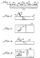
- a mandrel 10 is formed of a sheet of metal, such as a stainless steel having a thickness on the order of 1/16 of an inch for example, and having dimensions suitable for making one or a plurality of parts.
- the stainless steel mandrel 10 is initially provided with a non-conductive coating, such as Teflon 12, which is then ablated, as shown in FIG. 1, as by use of a laser, for example, to form a positive pattern of grooves, such as grooves 14a, 14b and 14c in the Teflon.
- the pattern of grooves exposes the conductive surface of the stainless steel mandrel and leaves a negative pattern of the electrically non-conductive Teflon on the mandrel working surface.
- one or more depressions 24a,24b are formed in the surface of the stainless steel mandrel 10 at areas, such as 14a and 14b, by means of photolithographic processes, employing a suitable photoresist coating, which is masked, exposed and developed, and then subjecting the mandrel to an etching bath to form the depression on the working surface of the mandrel.
- control of the shape of the depression is a significant feature of the present invention. Adequate control of this shape is not possible with the prior etching process. Therefore, in order to more precisely control the shape of the depressions 24a and 24b to any one of a number of different predetermined shapes, there is used an indentation tool, such as that shown for example in FIGS. 2 and 3.
- This tool includes a hardened steel base 16 and a shaped tapered projection 18 that is fixedly secured by any suitable means to the base 16.
- the projection 18 may be a pin fixed to the base that has been ground or otherwise machined to provide the illustrated shape.
- the shape of the indenting feature 18 of the tool is a cone, having a predetermined cone angle.
- Tool 16 is used to form the indentations 24a, 24b in the surface of the mandrel 10, as, for example, by mounting the tool on a carriage (not shown) supported over the mandrel for precision motion in orthogonal X and Y directions.
- the tool and its indentation feature which is pointing down toward the mandrel, are moved to a predetermined position and then the hardened tool and its tapered indentation feature are pressed against the mandrel to form the indentation.
- the tool is then raised and precisely moved to a second location, and a second indentation is formed. This procedure is repeated.
- a group of indentations are formed on the mandrel in any given pattern, with the location of the several indentations precisely positioned according to the degree of precision available from the X,Y drive of the tool carrying carriage.
- the tip 20 of the projecting feature 18 may be removed, as by grinding, clipping or the like, to provide a shape of projection feature having a tapered body and a very small area flat surface on its free end.
- the small area, substantially a flat free end, is illustrated by the dotted line in FIG. 2.
- the tapered indentations may have a base of about 10 mils in diameter, a tip area of about 5 mils diameter, and the height of the projection 18 may be 8 mils.
- the projecting features are used as contacts on a test probe they may be made considerably smaller so that the base of the projection may be in the order of 2 to 3 mils, with the top area having a diameter of about 1.0 mils. In such a test probe fixture the height of the tapered projecting contacts may be 1/2 to 4 mils.
- the hardened tool steel base plate 26 is formed with a rigid tapered pyramidal projection 28 fixedly secured thereto. While the drawing shows a pyramid with a base that is square, other shapes may be used (such as diamond). A different number of sides (such as three, forming a tetrahedron) may be used.
- the pyramidal projection if deemed necessary or desirable, may have a portion of its tip removed to provide a small area tip at its free end.
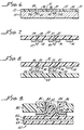
- the mandrel with its depressions is subjected to an electroforming processing such as electrolytic plating to electrodeposit a layer of copper or other suitable conductive material over the entire exposed conductive surface of the mandrel.
- an electroforming processing such as electrolytic plating to electrodeposit a layer of copper or other suitable conductive material over the entire exposed conductive surface of the mandrel.
- a depression such as depressions 37,39 (FIG. 6) will be formed in the pads 36,38, which create a tapered projection feature that lines the depression and is effectively hollow to some extent. For small projection features, subsequent lamination steps will fill the feature with dielectric material.
- these depressions may be filled with an epoxy 41,43 (FIG. 7) that hardens to a solid to strengthen the resulting projecting contact.
- Steps in the processing of the circuit that follow are the same as those described in the aforementioned co-pending application for Three-Dimensional Electroformed Circuitry. These following steps include the lamination of a dielectric substrate 32 to the subassembly of mandrel, Teflon and circuit traces of FIG. 6. Thereafter the assembly of substrate 32, together with the circuit traces 34 and pads 36,38 with their tapered projecting contacts 40,42, are removed as a unit from the mandrel 10 to result in the assembly illustrated in FIG. 7. An insulating coverlay may then be deposited over the exposed circuitry, leaving tips of the projections free of the insulation.
- FIG. 8 illustrates application of the described shaped contacts for use in a test probe.
- FIG. 8 shows a part of a test probe as including the dielectric substrate 32 with its pattern of circuit traces illustrated by trace 34, and its pattern of pointed connecting contacts illustrated in FIG. 8 by contacts 40 and 42.
- An integrated circuit wafer 54 having a plurality of test contact pads 56,58, is brought into close proximity to the test probe, with the contact pads 56,58 of the wafer 54 in registration with the corresponding pattern of tapered pointed contact features 40,42.
- the test probe is then pressed against the wafer to cause the pointed test probe contacts 40,42 to penetrate at their pointed free ends any surface contamination or oxide layer on the surface of contacts 54,56 to form a good electrical contact between the test probe and the integrated circuit wafer 54.
- a first circuit 60 formed as described in connection with FIGS. 1 through 7 above, is provided as including a pointed tapered projecting hollow contact 62, filled with an epoxy 63 and having a small area flat upper end 64.
- the projecting contact and its pad are formed on a substrate having a first dielectric layer 66 and a second dielectric layer 68 between which is sandwiched an electrical ground layer 70.
- the projecting contacts may be larger, as mentioned above, then the projecting contacts of a test probe.
- a circuit to which the circuit 60 of FIG. 9 is to be connected includes a dielectric substrate 80 bearing circuitry (not shown) and having a hole 82 which is through-hole plated with a conductive material, such as a metal 84, wherein the metal plating of the through hole includes flanges 86,88 extending radially outwardly from the hole on both sides of the substrate 80.
- the hole plating has relatively sharp corners 85 at the inner end of flanges 86.
- the one or more tapered and pointed projecting connectors are formed in a pattern that is identical to the pattern of holes 82.
- the two circuits With the projecting connecting features in registration with the holes, the two circuits are pressed against one another to cause the tapered projections to partly enter the holes. As the projection features enter the holes their tapered surfaces wedge the projection features into the holes, slightly deforming the hole edges or corners, as indicated at 90, to perform the equivalent of a wiping action that ensures a good solid electrical connecting contact despite any non-conductive oxidation coating that may have formed on the hole plating. Where the tapered projection is of pyramidal shape, having relatively sharp edges, such sharp edges even further facilitate and enhance the wedging action and the penetration of foreign surface layers of poorly conductive material, such as oxides. This wiping and wedging action causes penetration of oxide coatings of both the hole plating and the projecting contact surfaces.
- the two circuits may be either clamped together or held together in any other suitable manner, such as, for example, by use of pressure sensitive adhesive.
- the angle of the sides of the pyramidal or conical projection may be varied so as to control the nature of the wedging action and to obtain an optimum wiping action as the tapered projecting connective features penetrate the holes.
- a through hole is illustrated in FIG. 9, it will be readily appreciated that for those circuits embodying thicker substrates or for multiple layers of circuit boards stacked to one another, the hole into which the tapered contact is pressed need not be a through hole.
- circuits having fixed shaped contacts where the shapes are uniquely adapted for improving electrical contact without requiring any wiping action for good electrical connections.
- the contacts may be made in any suitable predetermined shape by use of an appropriately shaped indentation tool.
- Useful shapes include conical and pyramidal shapes, including truncated versions of these, and also spherical or near spherical shapes or bullet shapes that permit a conventional wiping action while tolerating some misalignment of contacts.
- an electric circuit connection component comprises a substrate, a plurality of electrical conductors lying in a plane on said substrate, and a plurality of electro-formed raised contacts on said substrate, each said contact being electrically connected to a respective one of said conductors and projecting from said plane to a contact free end that is shaped to penetrate a foreign material on the surface of a contact pad of a circuit to be connected to the connection component.
- Each said raised contact is electroformed on a respective one of the conductors with a pointed free end.
- the method of forming three-dimensional electrical circuitry having conductive components and at least one pointed projecting feature projecting from said components comprises: (a) forming an electrically conductive mandrel having a working surface, (b) forming a pattern of electrically non-conductive material on said mandrel, said material having a non-conductive material surface that divides said mandrel working surface into an electrically conductive pattern, (c) forming a depression in said mandrel working surface having a configuration that tapers from a broad area at said surface to a smaller area below said surface to define a pointed mandrel feature, (d) electro-forming a pattern of conductors and a pointed circuit feature on the conductive pattern of said working surface and in said pointed mandrel feature, (e) laminating a dielectric material upon said mandrel, upon said pattern of conductors and upon said pointed circuit feature to position said dielectric material over said conductors and circuit feature, whereby said conductors are bonded to said dielectric material and whereby said pointed
- an electrical circuit for connection to a second electrical circuit comprises a dielectric substrate, a pattern of conductive traces on one side of said substrate and positioned substantially on the surface of said one side, said traces collectively lying in and defining a trace surface, and at least one of said conductive traces having a three-dimensional conductive circuit feature formed integrally therewith and projecting from said trace surface, said feature having a free end that is shaped to enable penetration of an oxide coating or the like on the surface of a contact pad of said second circuit.
- the method of making such an electrical circuit connection component comprises the steps of (a) forming a shaped tool having a predetermined contact shape, (b) pressing said shaped tool into an electrically conductive mandrel to form a depression in the surface of the mandrel having the shape of said tool, (c) forming a conductive contact pad on said mandrel surface around said depression, said pad having a portion at least lining said depression to define a contact projecting from said pad and having said predetermined contact shape, (d) forming a dielectric substrate on said mandrel surface extending over said pad and bonded thereto, and (e) separating said mandrel from said substrate and pad.
- step of forming circuit traces on said mandrel surface said step of forming a substrate comprising bonding said substrate to said traces.
- an assembly of interconnected electrical circuits comprises a first circuit including a first substrate having a circuit trace thereon, a hole extending into said substrate, and a layer of conductive material lining the hole and connected to said trace, and a second circuit including a second substrate having a second circuit trace thereon, and a tapered contact connected to said trace and having a tapered end projecting from said second substrate into said hole in electrical contact with said layer of conductive material.
- an electrical circuit connection comprises a first conductive component having a surface bearing a low conductivity material, a second conductive component having an electrical circuit including a circuit trace and a pointed contact formed integrally with said circuit trace, said contact having a small area tip penetrating said material to press against said surface of said first conductive component.
- shaped contacts 40, 42 for interconnecting circuits or for use in an integrated circuit test probe are electroplated as integral parts of circuit traces 34 upon a stainless steel mandrel 10.
- a shaped, hardened steel indentation tool 16, 18, 26, 28 makes indentations 24a, 24b of predetermined shape in the surface of the mandrel 10, which is provided with a pattern of dielectric, such as Teflon 12, or photoresist.
- Areas of the steel mandrel, including the indentations 24a, 24b, are electroplated with a pattern of conductive material 34, 36, 38, and a dielectric substrate 32 is laminated to the conductive material.
- the circuit features formed by the indentations define raised contacts of a conical 18 or pyramidal 28 shape, having free ends with a small area that allows higher pressures to be applied to a surface against which the contacts are pressed. This enables the contacts to penetrate foreign materials, such as oxides, that may form on the surface of the pads 56, 58, to which the contacts are to be connected to ensure a good contact without any need for wiping action.
- the projecting contacts can also be pressed into plated holes 82, 84 in a substrate, such as a printed wiring board, to which mateable/demateable electric connection is to be made.
Landscapes
- Engineering & Computer Science (AREA)
- Manufacturing & Machinery (AREA)
- Microelectronics & Electronic Packaging (AREA)
- Physics & Mathematics (AREA)
- General Physics & Mathematics (AREA)
- Manufacturing Of Printed Wiring (AREA)
- Measuring Leads Or Probes (AREA)
- Testing Or Measuring Of Semiconductors Or The Like (AREA)
Applications Claiming Priority (4)
| Application Number | Priority Date | Filing Date | Title |
|---|---|---|---|
| US75084291A | 1991-08-26 | 1991-08-26 | |
| US750842 | 1991-08-26 | ||
| US07/753,400 US5207887A (en) | 1991-08-30 | 1991-08-30 | Semi-additive circuitry with raised features using formed mandrels |
| US753400 | 2001-01-03 |
Publications (3)
| Publication Number | Publication Date |
|---|---|
| EP0529577A2 true EP0529577A2 (de) | 1993-03-03 |
| EP0529577A3 EP0529577A3 (en) | 1993-08-04 |
| EP0529577B1 EP0529577B1 (de) | 1996-10-09 |
Family
ID=27115327
Family Applications (2)
| Application Number | Title | Priority Date | Filing Date |
|---|---|---|---|
| EP19920114444 Expired - Lifetime EP0529577B1 (de) | 1991-08-26 | 1992-08-25 | Elektrischer Messfühler mit geformten Kontakten |
| EP19920114445 Expired - Lifetime EP0529578B1 (de) | 1991-08-26 | 1992-08-25 | Semi-additive elektrische Schaltungen mit erhöhten Einzelheiten unter Verwendung geformter Matrizen |
Family Applications After (1)
| Application Number | Title | Priority Date | Filing Date |
|---|---|---|---|
| EP19920114445 Expired - Lifetime EP0529578B1 (de) | 1991-08-26 | 1992-08-25 | Semi-additive elektrische Schaltungen mit erhöhten Einzelheiten unter Verwendung geformter Matrizen |
Country Status (2)
| Country | Link |
|---|---|
| EP (2) | EP0529577B1 (de) |
| DE (2) | DE69214389T2 (de) |
Cited By (10)
| Publication number | Priority date | Publication date | Assignee | Title |
|---|---|---|---|---|
| EP0622981A1 (de) * | 1993-04-27 | 1994-11-02 | Hitachi Chemical Co., Ltd. | Leiterplatte für elektrische Prüfung und Verfahren zur Herstellung derselben |
| US5426850A (en) * | 1991-11-29 | 1995-06-27 | Hitachi Chemical Company, Ltd. | Fabrication process of wiring board |
| US5504992A (en) * | 1991-11-29 | 1996-04-09 | Hitachi Chemical Company, Ltd. | Fabrication process of wiring board |
| US5525065A (en) * | 1993-12-17 | 1996-06-11 | Hughes Aircraft Company | Cavity and bump interconnection structure for electronic packages |
| EP0764352A4 (de) * | 1994-06-07 | 2000-03-15 | Tessera Inc | Mikroelektronische kontakte und zusammenbauten |
| US6133534A (en) * | 1991-11-29 | 2000-10-17 | Hitachi Chemical Company, Ltd. | Wiring board for electrical tests with bumps having polymeric coating |
| EP1005086A3 (de) * | 1998-11-26 | 2001-01-03 | Shinko Electric Industries Co. Ltd. | Metallfolie mit Hockerkontakten, Schaltungssubstrat mit der Metallfolie, und Halbleitervorrichtung mit dem Schaltungssubstrat |
| US6205660B1 (en) | 1994-06-07 | 2001-03-27 | Tessera, Inc. | Method of making an electronic contact |
| SG80101A1 (en) * | 1999-06-28 | 2001-04-17 | Advantest Corp | Method of producing a contact structure |
| US6568073B1 (en) | 1991-11-29 | 2003-05-27 | Hitachi Chemical Company, Ltd. | Process for the fabrication of wiring board for electrical tests |
Family Cites Families (9)
| Publication number | Priority date | Publication date | Assignee | Title |
|---|---|---|---|---|
| NL108173C (de) * | 1954-06-25 | |||
| US3350250A (en) * | 1962-03-21 | 1967-10-31 | North American Aviation Inc | Method of making printed wire circuitry |
| US4125441A (en) * | 1978-01-30 | 1978-11-14 | General Dynamics Corporation | Isolated bump circuitry on tape utilizing electroforming |
| GB2049297B (en) * | 1979-05-18 | 1984-01-25 | Pactel Corp | Method of manufacturing printed circuitry |
| US4374708A (en) * | 1980-02-28 | 1983-02-22 | General Dynamics, Pomona Division | Fine line circuitry probes and method of manufacture |
| US4564423A (en) * | 1984-11-28 | 1986-01-14 | General Dynamics Pomona Division | Permanent mandrel for making bumped tapes and methods of forming |
| US4584039A (en) * | 1984-12-26 | 1986-04-22 | Hughes Aircraft Co. | Fine line flexible cable fabrication process |
| US4878294A (en) * | 1988-06-20 | 1989-11-07 | General Dynamics Corp., Pomona Division | Electroformed chemically milled probes for chip testing |
| FR2643754B1 (fr) * | 1989-02-28 | 1993-09-17 | Thomson Brandt Armements | Procede de realisation d'une connexion a plat |
-
1992
- 1992-08-25 DE DE1992614389 patent/DE69214389T2/de not_active Expired - Fee Related
- 1992-08-25 EP EP19920114444 patent/EP0529577B1/de not_active Expired - Lifetime
- 1992-08-25 EP EP19920114445 patent/EP0529578B1/de not_active Expired - Lifetime
- 1992-08-25 DE DE1992607996 patent/DE69207996T2/de not_active Expired - Fee Related
Cited By (14)
| Publication number | Priority date | Publication date | Assignee | Title |
|---|---|---|---|---|
| US6133534A (en) * | 1991-11-29 | 2000-10-17 | Hitachi Chemical Company, Ltd. | Wiring board for electrical tests with bumps having polymeric coating |
| US5426850A (en) * | 1991-11-29 | 1995-06-27 | Hitachi Chemical Company, Ltd. | Fabrication process of wiring board |
| US5504992A (en) * | 1991-11-29 | 1996-04-09 | Hitachi Chemical Company, Ltd. | Fabrication process of wiring board |
| US6568073B1 (en) | 1991-11-29 | 2003-05-27 | Hitachi Chemical Company, Ltd. | Process for the fabrication of wiring board for electrical tests |
| EP0622981A1 (de) * | 1993-04-27 | 1994-11-02 | Hitachi Chemical Co., Ltd. | Leiterplatte für elektrische Prüfung und Verfahren zur Herstellung derselben |
| KR100278460B1 (ko) * | 1993-04-27 | 2001-01-15 | 이사오 우치가사키 | 전기 테스트용 배선 기판 및 그 제조법 |
| US5525065A (en) * | 1993-12-17 | 1996-06-11 | Hughes Aircraft Company | Cavity and bump interconnection structure for electronic packages |
| EP0658960A3 (de) * | 1993-12-17 | 1997-01-29 | Hughes Aircraft Co | Hohlraum und Höckerverbindungsstruktur für elektronische Baugruppen. |
| EP0764352A4 (de) * | 1994-06-07 | 2000-03-15 | Tessera Inc | Mikroelektronische kontakte und zusammenbauten |
| US6205660B1 (en) | 1994-06-07 | 2001-03-27 | Tessera, Inc. | Method of making an electronic contact |
| US6938338B2 (en) | 1994-06-07 | 2005-09-06 | Tessera, Inc. | Method of making an electronic contact |
| EP1005086A3 (de) * | 1998-11-26 | 2001-01-03 | Shinko Electric Industries Co. Ltd. | Metallfolie mit Hockerkontakten, Schaltungssubstrat mit der Metallfolie, und Halbleitervorrichtung mit dem Schaltungssubstrat |
| US6420664B1 (en) | 1998-11-26 | 2002-07-16 | Shinko Electric Industries, Co., Ltd. | Metal foil having bumps, circuit substrate having the metal foil, and semiconductor device having the circuit substrate |
| SG80101A1 (en) * | 1999-06-28 | 2001-04-17 | Advantest Corp | Method of producing a contact structure |
Also Published As
| Publication number | Publication date |
|---|---|
| DE69207996D1 (de) | 1996-03-14 |
| EP0529577A3 (en) | 1993-08-04 |
| EP0529577B1 (de) | 1996-10-09 |
| EP0529578A2 (de) | 1993-03-03 |
| DE69207996T2 (de) | 1996-09-19 |
| EP0529578B1 (de) | 1996-01-31 |
| DE69214389D1 (de) | 1996-11-14 |
| EP0529578A3 (en) | 1993-08-04 |
| DE69214389T2 (de) | 1997-04-30 |
Similar Documents
| Publication | Publication Date | Title |
|---|---|---|
| US5307561A (en) | Method for making 3-D electrical circuitry | |
| US5197184A (en) | Method of forming three-dimensional circuitry | |
| US5747358A (en) | Method of forming raised metallic contacts on electrical circuits | |
| US5180311A (en) | Resilient interconnection bridge | |
| US5364277A (en) | Three-dimensional electroformed circuitry | |
| US5451169A (en) | Connector with monolithic multi-contact array | |
| US5072520A (en) | Method of manufacturing an interconnect device having coplanar contact bumps | |
| US20100075514A1 (en) | Method of making electrical connector on a flexible carrier | |
| US6256879B1 (en) | Compression connector | |
| EP0529577A2 (de) | Elektrischer Messfühler mit geformten Kontakten | |
| US5261158A (en) | Method of forming a resilient interconnection bridge | |
| US4107836A (en) | Circuit board with self-locking terminals | |
| US4187388A (en) | Circuit board with self-locking terminals | |
| US6641406B1 (en) | Flexible connector for high density circuit applications | |
| US5924193A (en) | Method of making mandrels and circuits therefrom | |
| US6230402B1 (en) | Electrical contact termination for a flexible circuit | |
| US5158466A (en) | Metallically encapsulated elevated interconnection feature | |
| CN118946034A (zh) | 一种具有金手指的线路板制造工艺及线路板 | |
| CA1291274C (en) | Wire/disk board-to-board interconnect device | |
| EP0610631A1 (de) | Elektrischer Verbinder | |
| EP1494516A2 (de) | Leiterplatte und Verfahren zu deren Herstellung | |
| CN223624751U (zh) | 一种垂直导电胶 | |
| JPH11108954A (ja) | コンタクトプローブ | |
| US6317974B1 (en) | Methods for creating wear resistant contact edges | |
| CN119895272A (zh) | 探针卡用悬臂式探针以及探针卡 |
Legal Events
| Date | Code | Title | Description |
|---|---|---|---|
| PUAI | Public reference made under article 153(3) epc to a published international application that has entered the european phase |
Free format text: ORIGINAL CODE: 0009012 |
|
| AK | Designated contracting states |
Kind code of ref document: A2 Designated state(s): DE FR GB |
|
| RIN1 | Information on inventor provided before grant (corrected) |
Inventor name: SCHREIBER, CHRISTOPHER M. Inventor name: CRUMLY, WILLIAM R. Inventor name: FEIGENBAUM, HAIM |
|
| PUAL | Search report despatched |
Free format text: ORIGINAL CODE: 0009013 |
|
| AK | Designated contracting states |
Kind code of ref document: A3 Designated state(s): DE FR GB |
|
| 17P | Request for examination filed |
Effective date: 19940119 |
|
| 17Q | First examination report despatched |
Effective date: 19950516 |
|
| GRAH | Despatch of communication of intention to grant a patent |
Free format text: ORIGINAL CODE: EPIDOS IGRA |
|
| GRAH | Despatch of communication of intention to grant a patent |
Free format text: ORIGINAL CODE: EPIDOS IGRA |
|
| GRAA | (expected) grant |
Free format text: ORIGINAL CODE: 0009210 |
|
| AK | Designated contracting states |
Kind code of ref document: B1 Designated state(s): DE FR GB |
|
| REF | Corresponds to: |
Ref document number: 69214389 Country of ref document: DE Date of ref document: 19961114 |
|
| ET | Fr: translation filed | ||
| PGFP | Annual fee paid to national office [announced via postgrant information from national office to epo] |
Ref country code: FR Payment date: 19970710 Year of fee payment: 6 |
|
| PGFP | Annual fee paid to national office [announced via postgrant information from national office to epo] |
Ref country code: GB Payment date: 19970717 Year of fee payment: 6 |
|
| PGFP | Annual fee paid to national office [announced via postgrant information from national office to epo] |
Ref country code: DE Payment date: 19970723 Year of fee payment: 6 |
|
| PLBE | No opposition filed within time limit |
Free format text: ORIGINAL CODE: 0009261 |
|
| 26N | No opposition filed | ||
| PG25 | Lapsed in a contracting state [announced via postgrant information from national office to epo] |
Ref country code: GB Free format text: LAPSE BECAUSE OF NON-PAYMENT OF DUE FEES Effective date: 19980825 |
|
| GBPC | Gb: european patent ceased through non-payment of renewal fee |
Effective date: 19980825 |
|
| PG25 | Lapsed in a contracting state [announced via postgrant information from national office to epo] |
Ref country code: FR Free format text: LAPSE BECAUSE OF NON-PAYMENT OF DUE FEES Effective date: 19990430 |
|
| PG25 | Lapsed in a contracting state [announced via postgrant information from national office to epo] |
Ref country code: DE Free format text: LAPSE BECAUSE OF NON-PAYMENT OF DUE FEES Effective date: 19990601 |
|
| REG | Reference to a national code |
Ref country code: FR Ref legal event code: ST |