EP0529959A2 - Capteur magnétorésistif - Google Patents
Capteur magnétorésistif Download PDFInfo
- Publication number
- EP0529959A2 EP0529959A2 EP92307640A EP92307640A EP0529959A2 EP 0529959 A2 EP0529959 A2 EP 0529959A2 EP 92307640 A EP92307640 A EP 92307640A EP 92307640 A EP92307640 A EP 92307640A EP 0529959 A2 EP0529959 A2 EP 0529959A2
- Authority
- EP
- European Patent Office
- Prior art keywords
- thin film
- layer
- magnetoresistive sensor
- magnetic
- ferromagnetic
- Prior art date
- Legal status (The legal status is an assumption and is not a legal conclusion. Google has not performed a legal analysis and makes no representation as to the accuracy of the status listed.)
- Withdrawn
Links
Images





Classifications
-
- G—PHYSICS
- G01—MEASURING; TESTING
- G01R—MEASURING ELECTRIC VARIABLES; MEASURING MAGNETIC VARIABLES
- G01R33/00—Arrangements or instruments for measuring magnetic variables
- G01R33/02—Measuring direction or magnitude of magnetic fields or magnetic flux
- G01R33/06—Measuring direction or magnitude of magnetic fields or magnetic flux using galvano-magnetic devices
-
- G—PHYSICS
- G01—MEASURING; TESTING
- G01R—MEASURING ELECTRIC VARIABLES; MEASURING MAGNETIC VARIABLES
- G01R33/00—Arrangements or instruments for measuring magnetic variables
- G01R33/02—Measuring direction or magnitude of magnetic fields or magnetic flux
- G01R33/06—Measuring direction or magnitude of magnetic fields or magnetic flux using galvano-magnetic devices
- G01R33/09—Magnetoresistive devices
- G01R33/093—Magnetoresistive devices using multilayer structures, e.g. giant magnetoresistance sensors
-
- B—PERFORMING OPERATIONS; TRANSPORTING
- B82—NANOTECHNOLOGY
- B82Y—SPECIFIC USES OR APPLICATIONS OF NANOSTRUCTURES; MEASUREMENT OR ANALYSIS OF NANOSTRUCTURES; MANUFACTURE OR TREATMENT OF NANOSTRUCTURES
- B82Y10/00—Nanotechnology for information processing, storage or transmission, e.g. quantum computing or single electron logic
-
- B—PERFORMING OPERATIONS; TRANSPORTING
- B82—NANOTECHNOLOGY
- B82Y—SPECIFIC USES OR APPLICATIONS OF NANOSTRUCTURES; MEASUREMENT OR ANALYSIS OF NANOSTRUCTURES; MANUFACTURE OR TREATMENT OF NANOSTRUCTURES
- B82Y25/00—Nanomagnetism, e.g. magnetoimpedance, anisotropic magnetoresistance, giant magnetoresistance or tunneling magnetoresistance
-
- G—PHYSICS
- G11—INFORMATION STORAGE
- G11B—INFORMATION STORAGE BASED ON RELATIVE MOVEMENT BETWEEN RECORD CARRIER AND TRANSDUCER
- G11B5/00—Recording by magnetisation or demagnetisation of a record carrier; Reproducing by magnetic means; Record carriers therefor
- G11B5/127—Structure or manufacture of heads, e.g. inductive
- G11B5/33—Structure or manufacture of flux-sensitive heads, i.e. for reproduction only; Combination of such heads with means for recording or erasing only
- G11B5/39—Structure or manufacture of flux-sensitive heads, i.e. for reproduction only; Combination of such heads with means for recording or erasing only using magneto-resistive devices or effects
- G11B2005/3996—Structure or manufacture of flux-sensitive heads, i.e. for reproduction only; Combination of such heads with means for recording or erasing only using magneto-resistive devices or effects large or giant magnetoresistive effects [GMR], e.g. as generated in spin-valve [SV] devices
Definitions
- This invention relates in general to magnetic transducers for reading information signals from a magnetic medium and, in particular, to an improved magnetoresistive read transducer.
- the prior art discloses a magnetic transducer referred to as a magnetoresistive (MR) sensor or head which has been shown to be capable of reading data from a magnetic surface at great linear densities.
- An MR sensor detects magnetic field signals through the resistance changes of a read element made from a magnetic material as a function of the amount and direction of magnetic flux being sensed by the element.
- These prior art MR sensors operate on the basis of the anisotropic magnetoresistive (AMR) effect in which a component of the resistance varies as cos2 of the angle between the magnetization and the direction of current flow.
- AMR anisotropic magnetoresistive
- This invention provides a magnetoresistive sensor comprising a layered structure having at least one bilayer comprising a first thin film of ferromagnetic material in interfacial contact with a second thin film of nonferromagnetic metallic material, characterised by the bilayer comprising a third thin film of material within said first thin film of ferromagnetic material, said third thin film having a thickness of between a fraction of a monolayer and several monolayers and being located at a predetermined distance x from the interface between said first and said second thin film layers.
- a current flow is produced through the MR sensor, and the variations in resistivity of the MR sensor produced by rotation of the magnetization in the first thin film layer of ferromagnetic material is sensed as a function of the magnetic field being sensed.
- the MR sensor comprises a trilayer structure having a first and a second thin film layer of ferromagnetic material separated by and in interfacial contact with a third thin film of non-magnetic metallic material.
- a thin film layer of material is provided in either or both of the ferromagnetic layers.
- the MR sensor comprises a trilayer structure having a first and a second thin film layer of ferromagnetic material separated by and in interfacial contact with a third film of non-magnetic metallic material.
- a thin film layer of ferromagnetic material is provided at either or both of the interfaces between the ferromagnetic layers and the thin film layer of non-magnetic material.
- F is a thin layer of ferromagnetic material such as iron (Fe) or cobalt (Co) and NM is a non-magnetic spacer layer such as chromium (Cr) or copper (Cu).
- CM is a non-magnetic spacer layer such as chromium (Cr) or copper (Cu).
- Observation of large values of magnetoresistance in such multilayers is found for structures in which the F layers are exchange coupled antiparallel to one another via the NM layer.
- magnetic files in the range of several hundred Oe are required to obtain these changes in resistance.
- FIG. 1 A specific embodiment of a multilayered structure, according to the present invention, is shown in Fig. 1.
- the magnetoresistive (MR) sensor 10 shown in Fig. 1 comprises repeated bilayers of a thin layer of a ferromagnetic material 12 and a non-magnetic material 14.
- a thin layer of material 16 is located within the layer of ferromagnetic material 12 at a distance x from the interface between ferromagnetic layer 12 and non-magnetic layer 14.
- the addition of this thin layer of material 16 within the ferromagnetic layer 12 increases the magnitude of the magnetoresistance without substantially increasing the applied magnetic field.
- Another structure that has recently been identified comprises a sandwich structure of the form F1/MN/F2/AF. Low saturation fields have been obtained for these sandwich structures by exchange biasing the F2 layer with an antiferromagnetic (AF) layer such as MnFe. Values of MR in the range of 3-5% can be obtained for these structures for fields in the 10 Oe range. Other structures require a much larger saturation field, by a factor of approximately 5 times larger.
- AF antiferromagnetic
- FIG. 2 A specific embodiment of sandwich structure, according to the present invention, is shown in Fig. 2.
- the MR sensor 20 shown in Fig. 2 comprises a first layer of ferromagnetic material 22, a layer of non-magnetic material 24, a second layer of ferromagnetic material 26, and a layer of antiferromagnetic material 28. Electrical leads 29 are provided to form a circuit path between the MR sensor structure, current source 19 and sensing means 21. Other layers (not shown) may also be provided for various biasing fields, for example, as is known in the art.
- sensing means 21 provides circuits to sense the variations in voltage across the MR sensor produced by changes in resistance of the MR sensor due to rotation of the magnetization in the first ferromagnetic layer 22 as a function of the magnetic field being sensed.
- a thin layer of material 23 is located within the first layer of ferromagnetic material 22 at a distance x from the interface between ferromagnetic layer 22 and non-magnetic layer 24.
- a second thin layer of material 25 may also be located within the second layer of ferromagnetic material 26 at a distance y from the interface between ferromagnetic layer 26 and non-magnetic layer 24. The addition of these thin layers of material 23, 25 substantially increases the magnitude of the magnetoresistance with a low applied field.
- FIG. 3 A further embodiment of an MR sensor, according to the present invention, is shown in Fig. 3.
- the MR sensor 30 shown in Fig. 3 comprises a special case of the previously described embodiments in which the distance x and y is zero.
- This structure comprises a first layer of ferromagnetic material 32, a layer of non-magnetic material 34, and a second layer of ferromagnetic material 36.
- a thin layer of ferromagnetic material 33 is located at the interface between ferromagnetic layer 32 and the layer of non-magnetic material 34.
- a second thin layer of ferromagnetic material 35 may also be located at the interface between the second layer of ferromagnetic material 36 and the layer of non-magnetic material 34.
- thin layers of material 16, 23, 25, 33 and 35 The purpose of thin layers of material 16, 23, 25, 33 and 35 is to produce a localized region whose spin dependent scattering properties are different from the layer of ferromagnetic material into which the localized regions are introduced.
- the thin layers of material 16, 23, 25, 33 and 35 have a thickness of a fraction of a monolayer to several monolayers or more of material, so these layers will be referred to as nanolayers.
- the materials for the nanolayers are metallic, and their characteristics are chosen based on the ferromagnetic materials into which they are introduced.
- Tables 1,2 and 3 which report the residual resistivity and temperature dependence of resistivity for a number of impurities in nickel(Ni), Co, and Fe as well as spin dependent impurity, scattering resistivities.
- These tables provide examples of materials that are candidates for use as the nanolayers for the respective ferromagnetic materials, as well. These and other materials may also be chosen because of their spin dependent electron scattering properties derived from induced strain, or introduced defects, or caused by the change in electronic band structure that the nanolayer introduces. Note that some of these materials are ferromagnetic and some of these materials are non-magnetic. Only the ferromagnetic materials are suitable for use as thin film layers 33 and 35.
- a specific embodiment of multilayered structures as shown in Fig. 1 were produced with the ferromagnetic layer 12 formed of Fe, the non-magnetic layer 14 formed of Cr, and the nanolayer of material 16 was also formed of Cr.
- the structures were prepared on a silicon (Si) substrate with a Cr underlayer as follows: Si/Cr(30 ⁇ )/[Fe(X ⁇ )/Cr(1 ⁇ )/Fe(40-2X ⁇ )/Cr(1 ⁇ )/Fe(X ⁇ )/Cr(t cr )]30/ Cr(50 ⁇ )
- Films comprising Fe/Cr multilayers with thin Cr nanolayers placed within the Fe layers were deposited by r f sputtering on Si substrates, and the resistance as a function of applied field measured.
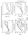
- the Cr nanolayers consisted of 1 ⁇ of material deposited within the Fe layer at at distance x from the Fe/Cr interface that was systematically varied from 0 to 17.5 ⁇ .
- Three series of films were deposited with the Cr layer thickness, t cr , of 10 ⁇ , 12.5 ⁇ , and 15 ⁇ . Note that, for films made within each of these three types, the only change is in the location of the nanolayer, and the total amount of each element is kept fixed. The results of the measurements on these structures is shown in Fig.
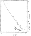
- the magnetoresistance values for a given saturation field obtained by nanolayering are consistently larger than those obtained from conventional Fe/Cr films. This is easily seen by plotting the magnetoresistance ⁇ R/R vs H 1/2 for films fabricated in each of these ways.
- This data shows that, by the addition of the nanolayer, an improvement by a factor of two in magnetoresistance is obtained, for a given saturation field, over that obtainable with any conventional Fe/Cr film.
- Fig. 6 This increase in magnetoresistance that can be obtained by this structure is graphically demonstrated in Fig. 6 in which the bottom curve shows the MR response for a structure without nanolayering and the top curve shows the MR response for the same structure with the addition of nanolayers.
- the structure for the bottom curve comprises: NiFeCo(70 ⁇ )/Cu(25 ⁇ )/NiFeCo(30 ⁇ )/MnFe(80 ⁇ )/Cu(10 ⁇ )
- the structure for the top curve comprises: NiFeCo(67 ⁇ )/Co(3 ⁇ )/Cu(25 ⁇ )/Co(3 ⁇ )/NiFeCo(27 ⁇ )/MnFe(80 ⁇ )/Cu(10 ⁇ )
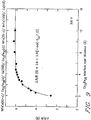
- Fig. 7 shows the dependence of the MR response on the thickness of the interface layer 23, 25 which in this embodiment is Co.
- the structure is of the same form as that considered in Fig. 6 and comprises: NiFe(60-X ⁇ )/Co(X ⁇ )/Cu(30 ⁇ )/Co(X ⁇ )/NiFe(25-X ⁇ )/MnFe(100 ⁇ )/Cu(10 ⁇ )
- Fig. 7 shows that the MR response increases rapidly with increasing Co thickness and then levels out with further increasing thickness. Increased Mr response has been noted for the thin interface layers from 0.5 to 20 ⁇ , and the preferred thickness range is from about 3 to about 20 ⁇ .
- Fig. 8 shows a comparison of the MR response for a Co/Cu/Co sandwich structure of the form: Co(60 ⁇ )/Cu(30 ⁇ )/Co(25 ⁇ )/MnFe(100 ⁇ )/Cu(10 ⁇ ) and a NiFe/Cu/NiFe/MnFe structure with a thin Co interface layer of the form: NiFe(55 ⁇ )/Co(5 ⁇ )/Cu(25 ⁇ )/Co(5 ⁇ )/NiFe(20 ⁇ )/MnFe(100 ⁇ )/Cu(10 ⁇ )
- Fig. 9 shows that the interface layer can also be an alloy rather than an elemental layer.
- This structure is of the form: NiFeCo(60-X ⁇ )/Co70Fe30(X ⁇ )/Cu(25 ⁇ )/Co70Fe30(XA)/NiFeCo(25-X ⁇ )/ MnFe(100 ⁇ )/Cu(10 ⁇ )
- This structure shows a similar dramatic increase in MR response with thickness of the Co70Fe30 layer.
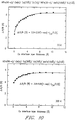
- Fig. 10 shows a comparison of a structure that has an interface layer at both interfaces with a similar structure which has an interface layer at one of the F/NM interfaces.
- the top figure shows data for a structure comprising: NiFe(60-X ⁇ )/Co(X ⁇ )/Cu(30 ⁇ )/Co(5X ⁇ )/NiFe(25-X ⁇ )/MnFe(100 ⁇ )Cu(10 ⁇ )
- the bottom figure shows data for a similar structure comprising: NiFe(80-X ⁇ )/Co(X ⁇ )/Cu(30 ⁇ )/Co(35 ⁇ )/MnFe(130 ⁇ )/Cu(10 ⁇ )
- the MR response only increases by 47% in this embodiment, approximately half the increase found in the top figure in which two interface layers were used.
- the MR response is still substantial for a structure in which a single interface layer in used, and the value remains high with increasing thickness of the interface layer as shown in Figs. 11 and 12.
- the MR response shown in Fig. 11 is for the following structure: Si/NiFe(80 ⁇ )/Co(10 ⁇ )/Cu(22 ⁇ )/Co(30 ⁇ )/FeMn(150 ⁇ )
- This structure shows an MR response of about 5. 3% with a 10 ⁇ Co interface layer.
- the MR response in Fig. 12 is for the following structure: Si/NiFe(60 ⁇ )/Co(20 ⁇ )/Cu(22 ⁇ )/Co(30 ⁇ )/FeMn(150 ⁇ )
- This structure shows an MR response of about 5.8% with a 20 ⁇ Co interface layer. This demonstrates that the useful range of thickness of the Co nanolayer is between about 3 ⁇ and about 20 ⁇ .
- magnetoresistive sensor comprising a layered structure having at least two bilayers each comprising a first thin film of ferromagnetic material in interfacial contact with a second thin film of nonferromagnetic metallic material
- a third thin film of material within said first thin films of ferromagnetic material said third thin film having a thickness of between a fraction of a monolayer and several monolayers and being located at a predetermined distance x from the interface between said first and said second thin film layers;
Landscapes
- Engineering & Computer Science (AREA)
- Physics & Mathematics (AREA)
- Chemical & Material Sciences (AREA)
- Nanotechnology (AREA)
- Crystallography & Structural Chemistry (AREA)
- Condensed Matter Physics & Semiconductors (AREA)
- General Physics & Mathematics (AREA)
- Mathematical Physics (AREA)
- Theoretical Computer Science (AREA)
- Hall/Mr Elements (AREA)
- Measuring Magnetic Variables (AREA)
- Magnetic Heads (AREA)
Applications Claiming Priority (2)
| Application Number | Priority Date | Filing Date | Title |
|---|---|---|---|
| US07/750,157 US5341261A (en) | 1991-08-26 | 1991-08-26 | Magnetoresistive sensor having multilayer thin film structure |
| US750157 | 1991-08-26 |
Publications (2)
| Publication Number | Publication Date |
|---|---|
| EP0529959A2 true EP0529959A2 (fr) | 1993-03-03 |
| EP0529959A3 EP0529959A3 (en) | 1993-11-03 |
Family
ID=25016745
Family Applications (1)
| Application Number | Title | Priority Date | Filing Date |
|---|---|---|---|
| EP19920307640 Withdrawn EP0529959A3 (en) | 1991-08-26 | 1992-08-21 | Magnetoresistive sensor |
Country Status (6)
| Country | Link |
|---|---|
| US (2) | US5341261A (fr) |
| EP (1) | EP0529959A3 (fr) |
| JP (1) | JP2654316B2 (fr) |
| KR (1) | KR960003994B1 (fr) |
| SG (1) | SG44397A1 (fr) |
| TW (1) | TW201357B (fr) |
Cited By (4)
| Publication number | Priority date | Publication date | Assignee | Title |
|---|---|---|---|---|
| EP0693791A1 (fr) * | 1994-07-21 | 1996-01-24 | Commissariat A L'energie Atomique | Capteur à magnétorésistance multicouche autopolarisée |
| US5667879A (en) * | 1995-09-13 | 1997-09-16 | Honeywell Inc. | TaN/NiFe/TaN anisotropic magnetic sensor element |
| US5875079A (en) * | 1996-03-15 | 1999-02-23 | Sony Corporation | Thin-film magnetic head with MR element hard and soft magnetic films having a weak exchange reciprocal action |
| EP0687917B1 (fr) * | 1994-06-15 | 2005-07-20 | International Business Machines Corporation | Capteur magnétorésistif à soupape de spin muni d'une couche laminée d'ancrage spontanée et système d'enregistrement magnétique utilisant le capteur |
Families Citing this family (64)
| Publication number | Priority date | Publication date | Assignee | Title |
|---|---|---|---|---|
| JP2725977B2 (ja) * | 1992-08-28 | 1998-03-11 | インターナショナル・ビジネス・マシーンズ・コーポレイション | 磁気抵抗センサ及びその製造方法、磁気記憶システム |
| US5780176A (en) * | 1992-10-30 | 1998-07-14 | Kabushiki Kaisha Toshiba | Magnetoresistance effect element |
| US5931032A (en) | 1998-04-16 | 1999-08-03 | Gregory; Edwin H. | Cutter and blow resistant lock |
| US5569544A (en) * | 1992-11-16 | 1996-10-29 | Nonvolatile Electronics, Incorporated | Magnetoresistive structure comprising ferromagnetic thin films and intermediate layers of less than 30 angstroms formed of alloys having immiscible components |
| JP3219329B2 (ja) * | 1993-02-03 | 2001-10-15 | 財団法人生産開発科学研究所 | 磁気抵抗効果素子 |
| US5493465A (en) * | 1993-03-15 | 1996-02-20 | Kabushiki Kaisha Toshiba | Magnetoresistance effect element and magnetic recording apparatus |
| US5408377A (en) * | 1993-10-15 | 1995-04-18 | International Business Machines Corporation | Magnetoresistive sensor with improved ferromagnetic sensing layer and magnetic recording system using the sensor |
| US5465185A (en) * | 1993-10-15 | 1995-11-07 | International Business Machines Corporation | Magnetoresistive spin valve sensor with improved pinned ferromagnetic layer and magnetic recording system using the sensor |
| SG52781A1 (en) * | 1994-02-21 | 1998-09-28 | Philips Electronics Nv | A method and a device for locally altering the magnetization direction in a body of magnetic material |
| EP0676746B1 (fr) * | 1994-03-09 | 1999-08-04 | Eastman Kodak Company | Tête de reproduction magnétorésistive à spin-valve duale |
| US5841611A (en) * | 1994-05-02 | 1998-11-24 | Matsushita Electric Industrial Co., Ltd. | Magnetoresistance effect device and magnetoresistance effect type head, memory device, and amplifying device using the same |
| US6256222B1 (en) | 1994-05-02 | 2001-07-03 | Matsushita Electric Industrial Co., Ltd. | Magnetoresistance effect device, and magnetoresistaance effect type head, memory device, and amplifying device using the same |
| US5491600A (en) * | 1994-05-04 | 1996-02-13 | International Business Machines Corporation | Multi-layer conductor leads in a magnetoresistive head |
| US5546253A (en) * | 1994-05-06 | 1996-08-13 | Quantum Corporation | Digitial output magnetoresistive (DOMR) head and methods associated therewith |
| US5561368A (en) * | 1994-11-04 | 1996-10-01 | International Business Machines Corporation | Bridge circuit magnetic field sensor having spin valve magnetoresistive elements formed on common substrate |
| JP2748876B2 (ja) * | 1995-01-27 | 1998-05-13 | 日本電気株式会社 | 磁気抵抗効果膜 |
| JPH0950613A (ja) * | 1995-08-03 | 1997-02-18 | Sony Corp | 磁気抵抗効果素子及び磁界検出装置 |
| US5896252A (en) * | 1995-08-11 | 1999-04-20 | Fujitsu Limited | Multilayer spin valve magneto-resistive effect magnetic head with free magnetic layer including two sublayers and magnetic disk drive including same |
| US5843589A (en) * | 1995-12-21 | 1998-12-01 | Hitachi, Ltd. | Magnetic layered material, and magnetic sensor and magnetic storage/read system based thereon |
| US6087027A (en) * | 1995-12-21 | 2000-07-11 | Hitachi, Ltd. | Magnetic layered material, and magnetic sensor and magnetic storage/read system based thereon |
| JPH09205234A (ja) * | 1996-01-26 | 1997-08-05 | Nec Corp | 磁気抵抗効果素子及び磁気抵抗効果センサ |
| US5747997A (en) * | 1996-06-05 | 1998-05-05 | Regents Of The University Of Minnesota | Spin-valve magnetoresistance sensor having minimal hysteresis problems |
| US6166539A (en) * | 1996-10-30 | 2000-12-26 | Regents Of The University Of Minnesota | Magnetoresistance sensor having minimal hysteresis problems |
| JPH1049834A (ja) * | 1996-08-07 | 1998-02-20 | Sony Corp | 多層磁気抵抗効果膜、磁気抵抗効果素子及び磁気抵抗効果型磁気ヘッド |
| US5739988A (en) * | 1996-09-18 | 1998-04-14 | International Business Machines Corporation | Spin valve sensor with enhanced magnetoresistance |
| US6249406B1 (en) | 1996-09-23 | 2001-06-19 | International Business Machines Corporation | Magnetoresistive sensor with a soft adjacent layer having high magnetization, high resistivity, low intrinsic anisotropy and near zero magnetostriction |
| US5731936A (en) * | 1996-09-26 | 1998-03-24 | International Business Machines Corporation | Magnetoresistive (MR) sensor with coefficient enhancing that promotes thermal stability |
| JP3528511B2 (ja) * | 1997-04-14 | 2004-05-17 | 松下電器産業株式会社 | 薄膜磁気ヘッド |
| US5748399A (en) * | 1997-05-13 | 1998-05-05 | International Business Machines Corporation | Resettable symmetric spin valve |
| US6118622A (en) | 1997-05-13 | 2000-09-12 | International Business Machines Corporation | Technique for robust resetting of spin valve head |
| US5825595A (en) * | 1997-05-13 | 1998-10-20 | International Business Machines Corporation | Spin valve sensor with two spun values separated by an insulated current conductor |
| US5880913A (en) * | 1997-10-27 | 1999-03-09 | International Business Machines Corporation | Antiparallel pinned spin valve sensor with read signal symmetry |
| WO1999022368A2 (fr) * | 1997-10-29 | 1999-05-06 | Koninklijke Philips Electronics N.V. | Detecteur de champ magnetique a jonction spin-tunnel |
| US6245450B1 (en) | 1997-11-17 | 2001-06-12 | Matsushita Electric Industrial Co., Ltd. | Exchange coupling film magnetoresistance effect device magnetoresistance effective head and method for producing magnetoresistance effect device |
| US6337215B1 (en) * | 1997-12-01 | 2002-01-08 | International Business Machines Corporation | Magnetic particles having two antiparallel ferromagnetic layers and attached affinity recognition molecules |
| US6108166A (en) * | 1998-03-12 | 2000-08-22 | Read-Rite Corporation | Current-pinned spin valve sensor |
| KR100334838B1 (ko) | 1998-07-21 | 2002-05-04 | 가타오카 마사타카 | 스핀밸브형 박막소자 및 그를 이용한 박막자기헤드 |
| US6052263A (en) * | 1998-08-21 | 2000-04-18 | International Business Machines Corporation | Low moment/high coercivity pinned layer for magnetic tunnel junction sensors |
| JP2000215414A (ja) | 1999-01-25 | 2000-08-04 | Hitachi Ltd | 磁気センサ― |
| US6208491B1 (en) * | 1999-05-26 | 2001-03-27 | International Business Machines Corporation | Spin valve with improved capping layer structure |
| US6226159B1 (en) | 1999-06-25 | 2001-05-01 | International Business Machines Corporation | Multilayered pinned layer of cobalt based films separated by a nickel base film for improved coupling field and GMR for spin valve sensors |
| US6783635B2 (en) | 1999-12-09 | 2004-08-31 | International Business Machines Corporation | Spin valve sensor free layer structure with a cobalt based layer that promotes magnetic stability and high magnetoresistance |
| US6508979B1 (en) * | 2000-02-08 | 2003-01-21 | University Of Southern California | Layered nanofabrication |
| US6583969B1 (en) * | 2000-04-12 | 2003-06-24 | International Business Machines Corporation | Pinned layer structure having nickel iron film for reducing coercivity of a free layer structure in a spin valve sensor |
| US6645614B1 (en) | 2000-07-25 | 2003-11-11 | Seagate Technology Llc | Magnetic recording media having enhanced coupling between magnetic layers |
| US6473278B1 (en) | 2000-07-31 | 2002-10-29 | International Business Machines Corporation | Giant magnetoresistive sensor with a high resistivity free layer |
| US6538859B1 (en) | 2000-07-31 | 2003-03-25 | International Business Machines Corporation | Giant magnetoresistive sensor with an AP-coupled low Hk free layer |
| US6580589B1 (en) | 2000-10-06 | 2003-06-17 | International Business Machines Corporation | Pinned layer structure for a spin valve sensor having cobalt iron (CoFe) and cobalt iron oxide (CoFeO) laminated layers |
| US6570745B1 (en) | 2000-11-20 | 2003-05-27 | International Business Machines Corporation | Lead overlaid type of sensor with sensor passive regions pinned |
| US6737172B1 (en) | 2000-12-07 | 2004-05-18 | Seagate Technology Llc | Multi-layered anti-ferromagnetically coupled magnetic media |
| US6689497B1 (en) | 2001-01-08 | 2004-02-10 | Seagate Technology Llc | Stabilized AFC magnetic recording media with reduced lattice mismatch between spacer layer(s) and magnetic layers |
| US6828036B1 (en) | 2001-08-21 | 2004-12-07 | Seagate Technology Llc | Anti-ferromagnetically coupled magnetic media with combined interlayer + first magnetic layer |
| GB2380046A (en) * | 2001-09-21 | 2003-03-26 | Hewlett Packard Co | Data storage media having integrated environmental sensor |
| JP3839697B2 (ja) | 2001-10-17 | 2006-11-01 | アルプス電気株式会社 | 回転角度センサ |
| US6567236B1 (en) | 2001-11-09 | 2003-05-20 | International Business Machnes Corporation | Antiferromagnetically coupled thin films for magnetic recording |
| US6815082B2 (en) | 2001-11-30 | 2004-11-09 | Seagate Technology Llc | Anti-ferromagnetically coupled perpendicular magnetic recording media |
| US7842409B2 (en) | 2001-11-30 | 2010-11-30 | Seagate Technology Llc | Anti-ferromagnetically coupled perpendicular magnetic recording media with oxide |
| US7221545B2 (en) * | 2004-02-18 | 2007-05-22 | Hitachi Global Storage Technologies Netherlands B.V. | High HC reference layer structure for self-pinned GMR heads |
| US7190560B2 (en) | 2004-02-18 | 2007-03-13 | Hitachi Global Storage Technologies Netherlands B.V. | Self-pinned CPP sensor using Fe/Cr/Fe structure |
| US7268982B2 (en) * | 2004-10-21 | 2007-09-11 | Hitachi Global Storage Technologies Netherlands B.V. | Current perpendicular to plane (CPP) GMR structure having vanadium doped, AP coupled, multi-layered pinned structure |
| US20060228586A1 (en) * | 2005-04-06 | 2006-10-12 | Seagate Technology Llc | Ferromagnetically coupled magnetic recording media |
| US7514271B2 (en) * | 2007-03-30 | 2009-04-07 | International Business Machines Corporation | Method of forming high density planar magnetic domain wall memory |
| KR101233662B1 (ko) * | 2011-07-19 | 2013-02-15 | 충남대학교산학협력단 | 유연 박막 자기저항 센서 및 그 제조 방법 |
| US11493573B2 (en) * | 2019-08-27 | 2022-11-08 | Western Digital Technologies, Inc. | Magnetic sensor with dual TMR films and the method of making the same |
Family Cites Families (13)
| Publication number | Priority date | Publication date | Assignee | Title |
|---|---|---|---|---|
| US4447839A (en) * | 1980-10-28 | 1984-05-08 | Compagnie Internationale Pour L'informatique Cii-Honeywell Bull (Societe Anonyme) | Magnetoresistant transducer |
| JPS62159317A (ja) * | 1986-01-08 | 1987-07-15 | Hitachi Ltd | 磁気抵抗効果型磁気ヘツド |
| JPH07105006B2 (ja) * | 1985-11-05 | 1995-11-13 | ソニー株式会社 | 磁気抵抗効果型磁気ヘツド |
| US4940511A (en) * | 1988-03-28 | 1990-07-10 | International Business Machines Corporation | Method for making a magnetoresistive read transducer |
| DE3820475C1 (fr) * | 1988-06-16 | 1989-12-21 | Kernforschungsanlage Juelich Gmbh, 5170 Juelich, De | |
| JPH0223679A (ja) * | 1988-07-12 | 1990-01-25 | Nec Corp | 磁気抵抗効果型素子 |
| JPH0223678A (ja) * | 1988-07-12 | 1990-01-25 | Nec Corp | 磁気抵抗効果型素子 |
| JPH02266579A (ja) * | 1989-04-07 | 1990-10-31 | Nec Corp | 磁気抵抗効果素子 |
| FR2648942B1 (fr) * | 1989-06-27 | 1995-08-11 | Thomson Csf | Capteur a effet magnetoresistif |
| JPH0427106A (ja) * | 1990-05-23 | 1992-01-30 | Tdk Corp | 鉄系磁性多層膜 |
| US5206590A (en) * | 1990-12-11 | 1993-04-27 | International Business Machines Corporation | Magnetoresistive sensor based on the spin valve effect |
| MY108176A (en) * | 1991-02-08 | 1996-08-30 | Hitachi Global Storage Tech Netherlands B V | Magnetoresistive sensor based on oscillations in the magnetoresistance |
| US5159513A (en) * | 1991-02-08 | 1992-10-27 | International Business Machines Corporation | Magnetoresistive sensor based on the spin valve effect |
-
1991
- 1991-08-26 US US07/750,157 patent/US5341261A/en not_active Expired - Lifetime
-
1992
- 1992-07-15 JP JP4187788A patent/JP2654316B2/ja not_active Expired - Lifetime
- 1992-08-18 KR KR1019920014823A patent/KR960003994B1/ko not_active Expired - Fee Related
- 1992-08-21 SG SG1996000143A patent/SG44397A1/en unknown
- 1992-08-21 EP EP19920307640 patent/EP0529959A3/en not_active Withdrawn
- 1992-10-14 TW TW081108173A patent/TW201357B/zh active
-
1994
- 1994-08-15 US US08/290,324 patent/US5598308A/en not_active Expired - Lifetime
Cited By (6)
| Publication number | Priority date | Publication date | Assignee | Title |
|---|---|---|---|---|
| EP0687917B1 (fr) * | 1994-06-15 | 2005-07-20 | International Business Machines Corporation | Capteur magnétorésistif à soupape de spin muni d'une couche laminée d'ancrage spontanée et système d'enregistrement magnétique utilisant le capteur |
| EP0693791A1 (fr) * | 1994-07-21 | 1996-01-24 | Commissariat A L'energie Atomique | Capteur à magnétorésistance multicouche autopolarisée |
| FR2722918A1 (fr) * | 1994-07-21 | 1996-01-26 | Commissariat Energie Atomique | Capteur a magnetoresistance multicouche autopolarisee |
| US5635835A (en) * | 1994-07-21 | 1997-06-03 | Commissariat A L'energie Atomique | Self biased multilayer magnetoresistance sensor |
| US5667879A (en) * | 1995-09-13 | 1997-09-16 | Honeywell Inc. | TaN/NiFe/TaN anisotropic magnetic sensor element |
| US5875079A (en) * | 1996-03-15 | 1999-02-23 | Sony Corporation | Thin-film magnetic head with MR element hard and soft magnetic films having a weak exchange reciprocal action |
Also Published As
| Publication number | Publication date |
|---|---|
| KR960003994B1 (ko) | 1996-03-25 |
| US5341261A (en) | 1994-08-23 |
| EP0529959A3 (en) | 1993-11-03 |
| SG44397A1 (en) | 1997-12-19 |
| US5598308A (en) | 1997-01-28 |
| JP2654316B2 (ja) | 1997-09-17 |
| TW201357B (fr) | 1993-03-01 |
| JPH05266436A (ja) | 1993-10-15 |
| KR930005276A (ko) | 1993-03-23 |
Similar Documents
| Publication | Publication Date | Title |
|---|---|---|
| US5341261A (en) | Magnetoresistive sensor having multilayer thin film structure | |
| KR100192192B1 (ko) | 자기저항 효과막, 이를 제조하는 방법 및 자기저항효과소자 | |
| US6295186B1 (en) | Spin-valve magnetoresistive Sensor including a first antiferromagnetic layer for increasing a coercive force and a second antiferromagnetic layer for imposing a longitudinal bias | |
| US5341118A (en) | Multilayer magnetic structure wherein the magnitude of the structure magnetoresistance is a function of nonmagnetic layer thickness | |
| US5955211A (en) | Magnetoresistive film | |
| EP0791915B1 (fr) | Dispositif magnétorésistif et tête magnétorésistive | |
| US5206590A (en) | Magnetoresistive sensor based on the spin valve effect | |
| US7046490B1 (en) | Spin valve magnetoresistance sensor and thin film magnetic head | |
| EP0681338B1 (fr) | Dispositif à magnétorésistance et tête à effet de magnétorésistance, dispositif de mémoire et amplificateur utilisant ce dispositif | |
| US5923504A (en) | Magnetoresistance device | |
| US5958611A (en) | Magnetic multilayered film, magnetoresistance effect element and magnetoresistance device | |
| US5891586A (en) | Multilayer thin-film for magnetoresistive device | |
| US5872502A (en) | Magnetoresistance effect film and production process thereof | |
| US7265948B2 (en) | Magnetoresistive element with oxide magnetic layers and metal magnetic films deposited thereon | |
| US5661449A (en) | Magnetic multilayer film, method for making, and magnetoresistance device | |
| GB2400719A (en) | Self-pinned CPP giant magnetoresistive head | |
| JPH1011723A (ja) | 磁気抵抗効果型トランスデューサ、その製造方法及び磁気記録装置 | |
| EP0814519B1 (fr) | Elément à effet magnétorésistif, son procédé de fabrication et tête magnétique de cela | |
| JPH04247607A (ja) | 磁気抵抗効果素子 | |
| GB2401715A (en) | CPP giant magnetoresistive element | |
| KR100304770B1 (ko) | 자기저항효과박막과그제조방법 | |
| US7554776B2 (en) | CCP magnetic detecting element including a self-pinned CoFe layer | |
| EP0624868B1 (fr) | Eléments magnéto-résistifs et procédé de fabrication | |
| KR100321956B1 (ko) | 자기저항효과막및그제조방법 | |
| US6215631B1 (en) | Magnetoresistive effect film and manufacturing method therefor |
Legal Events
| Date | Code | Title | Description |
|---|---|---|---|
| PUAI | Public reference made under article 153(3) epc to a published international application that has entered the european phase |
Free format text: ORIGINAL CODE: 0009012 |
|
| AK | Designated contracting states |
Kind code of ref document: A2 Designated state(s): DE FR GB |
|
| 17P | Request for examination filed |
Effective date: 19930624 |
|
| PUAL | Search report despatched |
Free format text: ORIGINAL CODE: 0009013 |
|
| AK | Designated contracting states |
Kind code of ref document: A3 Designated state(s): DE FR GB |
|
| 17Q | First examination report despatched |
Effective date: 19960226 |
|
| STAA | Information on the status of an ep patent application or granted ep patent |
Free format text: STATUS: THE APPLICATION HAS BEEN WITHDRAWN |
|
| 18W | Application withdrawn |
Withdrawal date: 19960626 |