EP0530107A1 - PSK-Demodulator mit Korrektur im Basisband für Phasen- oder Frequenzfehler - Google Patents
PSK-Demodulator mit Korrektur im Basisband für Phasen- oder Frequenzfehler Download PDFInfo
- Publication number
- EP0530107A1 EP0530107A1 EP92402357A EP92402357A EP0530107A1 EP 0530107 A1 EP0530107 A1 EP 0530107A1 EP 92402357 A EP92402357 A EP 92402357A EP 92402357 A EP92402357 A EP 92402357A EP 0530107 A1 EP0530107 A1 EP 0530107A1
- Authority
- EP
- European Patent Office
- Prior art keywords
- phase
- digital
- demodulation
- frequency
- signals
- Prior art date
- Legal status (The legal status is an assumption and is not a legal conclusion. Google has not performed a legal analysis and makes no representation as to the accuracy of the status listed.)
- Granted
Links
- 238000012545 processing Methods 0.000 claims abstract description 28
- 238000005070 sampling Methods 0.000 claims abstract description 19
- 230000001427 coherent effect Effects 0.000 claims abstract description 15
- 238000001514 detection method Methods 0.000 claims description 33
- 239000013256 coordination polymer Substances 0.000 claims description 26
- 230000004044 response Effects 0.000 claims description 20
- 230000006870 function Effects 0.000 claims description 14
- 230000015654 memory Effects 0.000 claims description 12
- 230000010363 phase shift Effects 0.000 claims description 9
- 230000003213 activating effect Effects 0.000 claims 1
- 239000011159 matrix material Substances 0.000 claims 1
- 230000001020 rhythmical effect Effects 0.000 claims 1
- 238000011084 recovery Methods 0.000 abstract description 20
- 239000000969 carrier Substances 0.000 abstract description 6
- 108010064535 CCAAT-Enhancer-Binding Protein-beta Proteins 0.000 abstract description 4
- 102100031621 Cysteine and glycine-rich protein 2 Human genes 0.000 abstract description 4
- 238000010586 diagram Methods 0.000 description 16
- 230000005540 biological transmission Effects 0.000 description 14
- 230000007704 transition Effects 0.000 description 13
- 238000004364 calculation method Methods 0.000 description 9
- 238000010200 validation analysis Methods 0.000 description 9
- 230000010354 integration Effects 0.000 description 8
- 238000000034 method Methods 0.000 description 6
- 230000033764 rhythmic process Effects 0.000 description 6
- 238000007493 shaping process Methods 0.000 description 4
- 239000013598 vector Substances 0.000 description 4
- 238000012423 maintenance Methods 0.000 description 3
- 102100031051 Cysteine and glycine-rich protein 1 Human genes 0.000 description 2
- 101710185487 Cysteine and glycine-rich protein 1 Proteins 0.000 description 2
- 101000935571 Drosophila melanogaster Bomanin Short 1 Proteins 0.000 description 2
- 230000003068 static effect Effects 0.000 description 2
- 230000004913 activation Effects 0.000 description 1
- 230000002457 bidirectional effect Effects 0.000 description 1
- 238000004891 communication Methods 0.000 description 1
- 238000013016 damping Methods 0.000 description 1
- 238000005516 engineering process Methods 0.000 description 1
- 230000002401 inhibitory effect Effects 0.000 description 1
- 230000000670 limiting effect Effects 0.000 description 1
- 230000004048 modification Effects 0.000 description 1
- 238000012986 modification Methods 0.000 description 1
- 230000036961 partial effect Effects 0.000 description 1
- 239000010453 quartz Substances 0.000 description 1
- 230000002829 reductive effect Effects 0.000 description 1
- 230000008929 regeneration Effects 0.000 description 1
- 238000011069 regeneration method Methods 0.000 description 1
- VYPSYNLAJGMNEJ-UHFFFAOYSA-N silicon dioxide Inorganic materials O=[Si]=O VYPSYNLAJGMNEJ-UHFFFAOYSA-N 0.000 description 1
- 238000012546 transfer Methods 0.000 description 1
- 238000002834 transmittance Methods 0.000 description 1
- 230000017105 transposition Effects 0.000 description 1
Images


Classifications
-
- H—ELECTRICITY
- H04—ELECTRIC COMMUNICATION TECHNIQUE
- H04L—TRANSMISSION OF DIGITAL INFORMATION, e.g. TELEGRAPHIC COMMUNICATION
- H04L27/00—Modulated-carrier systems
- H04L27/18—Phase-modulated carrier systems, i.e. using phase-shift keying
- H04L27/22—Demodulator circuits; Receiver circuits
- H04L27/233—Demodulator circuits; Receiver circuits using non-coherent demodulation
- H04L27/2332—Demodulator circuits; Receiver circuits using non-coherent demodulation using a non-coherent carrier
-
- H—ELECTRICITY
- H04—ELECTRIC COMMUNICATION TECHNIQUE
- H04L—TRANSMISSION OF DIGITAL INFORMATION, e.g. TELEGRAPHIC COMMUNICATION
- H04L27/00—Modulated-carrier systems
- H04L27/0014—Carrier regulation
- H04L2027/0024—Carrier regulation at the receiver end
- H04L2027/0026—Correction of carrier offset
- H04L2027/003—Correction of carrier offset at baseband only
-
- H—ELECTRICITY
- H04—ELECTRIC COMMUNICATION TECHNIQUE
- H04L—TRANSMISSION OF DIGITAL INFORMATION, e.g. TELEGRAPHIC COMMUNICATION
- H04L27/00—Modulated-carrier systems
- H04L27/0014—Carrier regulation
- H04L2027/0044—Control loops for carrier regulation
- H04L2027/0053—Closed loops
- H04L2027/0057—Closed loops quadrature phase
-
- H—ELECTRICITY
- H04—ELECTRIC COMMUNICATION TECHNIQUE
- H04L—TRANSMISSION OF DIGITAL INFORMATION, e.g. TELEGRAPHIC COMMUNICATION
- H04L27/00—Modulated-carrier systems
- H04L27/0014—Carrier regulation
- H04L2027/0044—Control loops for carrier regulation
- H04L2027/0071—Control of loops
- H04L2027/0075—Error weighting
- H04L2027/0077—Error weighting stop and go
Definitions
- the present invention relates to a coherent demodulation device and more particularly to means for recovering a carrier wave in the modulated signal received by the demodulation device.
- the demodulation device is included in a receiver of a digital transmission system, for example for digital communications between radio relays and / or by satellite.
- a digital data signal modulates a radio carrier.
- the modulation used can be a multiphase modulation or a multi-amplitude modulation.
- Multiphase modulation is a phase modulation with N states or symbols, where N is an integer equal to a power of 2; for example when N is equal to 4, 8 or 16, the phase modulation is designated by the abbreviation MDP4, MDP8, or MDP16.
- Multiamplitude modulation is known by the acronym MAQ meaning "amplitude modulation in quadrature" and combines two carriers in quadrature modulated respectively, for example with 2, 4 or 8 states or amplitude levels; multi-amplitude modulation thus offers for example 4, 16, or 64 states or symbols corresponding to the acronyms MAQ4, MAQ16 or MAQ64.
- modulation by two component signals originating from the digital signal to be modulated, modulating two waves in phase quadrature originating from the same carrier wave.
- the carrier frequency is greater than the symbol transmission frequency, also called the clock frequency 1 / T, T being the clock period.
- the modulated digital signal is generally transposed to the transmission frequency in the transmitter of the transmission system.
- frequency transposition and preamplification means receive the transmitted signal and apply the modulated multi-symbol signal at intermediate frequency to the demodulation device.
- the two parameters necessary to restore the digital signal transmitted by a transmitter are the phase and the frequency of the carrier wave.
- phase control techniques use phase control techniques. These circuits are made in the form of an analog phase locked loop (PLL) including a phase comparator, a filter and a voltage controlled oscillator.
- PLL phase locked loop
- the disadvantages associated with such embodiments are numerous. In terms of performance, compensation for a frequency difference between the demodulation carrier wave frequency provided by the voltage-controlled oscillator and the frequency of the modulation carrier wave in the transmitter is only done. in return for a phase error proportional to the frequency difference between the carrier waves and inversely proportional to the loop gain.
- the phase error having non-negligible consequences on the performance of the transmission system, it must be limited to low values, typically a few tenths of a degree, which requires increasing the loop gain. However, for reasons of stability of the loop, it cannot arbitrarily increase this gain.
- phase error Another consequence induced by this phase error is the limitation of the acquisition frequency range to frequency values compatible with an admissible static phase error.
- phase error consists of either a first error signal, well suited to weak phase errors, ie of a second error signal obtained following a preliminary processing which brings back all the points of the constellation relating to the chosen modulation (eg: MAQ 256) around the axis of positive abscissas in a Fresnel benchmark.
- This treatment consists of a phase shift of (90 x N - 45) °, N being the number of the dial concerned.
- the invention aims to remedy the drawbacks of known analog phase loops by providing carrier wave recovery means which are designed entirely in the form of digital circuits. Under these conditions, the recovery means are more easily integrated on the one hand, and have operating characteristics independent of the speed of modulation of the signal received on the other hand.
- a coherent demodulation device receiving a modulated signal obtained by multisymbol modulation of two quadrature modulation carrier waves, said device comprising demodulation means providing quadrature demodulation carrier waves for demodulating the modulated signal into two component signals demodulated analog, the quadrature demodulation carrier waves having a free frequency belonging to a frequency uncertainty range of the modulation carrier waves, is characterized by : sampling means operating at clock frequency of the symbols of the modulated signal to convert the two demodulated analog component signals into two incoming digital signals, digital phase shifting means for phase shifting the incoming signals by a digital demodulation phase into two outgoing digital signals, generalized digital comparison means receiving the two outgoing digital signals to produce transmitted error signal pulses, and digital processing means for calculating the digital demodulation phase as a function of the error signal pulses in order to compensate a posteriori for the phase and frequency differences between the modulation carrier waves and the demodulation carrier waves by phase shift of the incoming signals .
- the demodulation device only comprises, as analog circuits, the demodulation means with mixers and oscillator demodulating the modulated signal received by two carrier waves for quadrature demodulation.
- the oscillator in the demodulation means is a free oscillator, and no longer a voltage controlled oscillator. This facilitates the integration of the device and allows better characteristics to be obtained.
- phase loop essentially produced by the phase shifting means, the generalized comparison means and the processing means is entirely digital.
- This phase loop operating at the modulation frequency, it can be used for clock frequencies of several tens of MHz with conventional technologies.
- the generalized digital comparison means distinguish the phase tracking regime (or "frequency maintenance") during which a phase comparison between modulation carrier waves and demodulation carrier waves is carried out, and the frequency acquisition regime during which a frequency comparison between the carrier waves is carried out.
- the generalized comparison means comprise digital phase comparison means for producing, at the clock frequency, first and second error signal pulses respectively in response to negative and positive phase differences between the waves.
- demodulation carriers and modulation carriers digital frequency comparison means for producing, at the clock frequency, third and fourth error signal pulses respectively in response to positive and negative frequency differences between the demodulation carrier waves and modulation carrier waves, and state detection means for providing a detection pulse in response to amplitudes of the outgoing digital signals which are within predetermined respective amplitude intervals, during each period d symbol clock to generate a comm signal ande logic to activate the frequency comparison means and deactivate the phase comparison means when a count of detection pulses accumulated during a period multiple of the symbol period is greater than a first predetermined threshold, and to deactivate the means comparison frequency and activate the phase comparison means when said count of detection pulses accumulated during said multiple period is less than said first threshold.
- the state detection means which contribute to distinguishing the two regimes preferably comprise a circuit for producing one of said detection pulses when the amplitudes of the outgoing signals are included in the respective predetermined intervals during the clock period, a counter for counting the detection pulses during said multiple period, a comparator for comparing the count of detection pulses accumulated in the counter at said first predetermined threshold in order to produce a control logic signal whose two states are respectively representative of detection pulse counts above and below said first predetermined threshold, and switching means for switching error signal pulse outputs of the phase and frequency comparison means to inputs of the digital processing means as a function of the states of the control signal .
- the digital processing means comprise an up-down counter having an incrementable and decrementable content.
- the content is incremented and decremented respectively by the first and second error signal pulses produced by the generalized comparison means when said count of detection pulses accumulated in said counter during the multiple period is less than said first threshold.
- the content of the up-down counter is also incremented and decremented respectively by the third and fourth error signal pulses produced by the generalized comparison means when said count of detection pulses accumulated in said counter during said multiple period is greater than said first. threshold.
- the digital processing means also comprise addition-subtraction means for respectively adding the content of the up-down counter to a first predetermined parameter in response to one of said first and third pulses and for subtracting the content of the up-down counter from said first parameter in response to one of the second and fourth pulses, means for multiplying the result of the operation carried out by the addition-subtraction means by a second predetermined parameter, and means for accumulating the product supplied by the means for multiply at the clock frequency to produce a demodulation phase.
- the up-down counter performs a first error signal integration in a manner analogous to a loop filter, and the means for accumulating performs a second error signal integration, in a manner analogous to a voltage controlled oscillator .
- This double integration makes it possible to obtain a static zero phase error, regardless of the frequency difference to be compensated between the modulation and demodulation carrier waves.
- the demodulation device may also include means for periodically saving the content of the up-down counter when said count of detection pulses accumulated in said counter during the multiple period is less than said first threshold, and for introducing the content saved in the counter- down-counter when said count of detection pulses accumulated during the multiple period in said counter is greater than said first threshold.
- the means for saving contribute to obtaining a frequency acquisition range close to the maximum theoretical range, with very short acquisition periods.
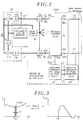
- a coherent demodulation device included in a receiver of a digital transmission system comprises a demodulation circuit CD and a carrier recovery circuit CRP1.
- the coherent demodulation device receives a modulation signal SI with a modulation carrier wave transmitted by a transmitter of a digital transmission system.
- the demodulation circuit CD comprises two mixers 11a and 11b acting as demodulators, two low-pass filters 12a and 12b, and a phase shifter of ( ⁇ / 2) 13.
- the carrier recovery circuit CRP1 comprises a phase comparator 15, a low-pass loop filter 16 and a voltage-controlled oscillator (VCO) 17, and may include, according to certain embodiments known to a person skilled in the art, a frequency acquisition aid (MAA) means 18 connected to the loop filter input 16.
- VCO voltage-controlled oscillator
- Two respective first inputs of the mixers 11a and 11b receive the modulated signal SI.
- a recovered carrier signal SP is applied to two second inputs of the mixers 11a and 11b respectively directly and through the phase shifter of ( ⁇ / 2) 13.
- Respective outputs of the mixers are connected to inputs of the comparator 15 through the filters 12a and 12b. Filters 12a and 12b reject harmonics in the vicinity of the frequency twice the carrier frequency in the demodulated signals delivered by the mixers.
- the phase comparator 15 produces an error signal ⁇ representative of the phase error instant between the recovered modulation carrier signal SP and the transmitted modulation carrier wave to be estimated.
- the oscillator 17 produces the recovered carrier signal SP controlled by the frequency and the phase of the modulation carrier wave in response to the error signal ⁇ generated at the output of the phase comparator 15 and applied to a control input. from oscillator 17 through loop filter 16.
- the role of the loop filter 16 consists in limiting the influence of the noise on the error signal ⁇ and in the rejection of the high frequency components in order to suitably control the oscillator 17.
- the baseband signals X and Y from the respective filters 12a and 12b correspond to the two component signals modulating the two carrier waves in quadrature in the transmitter. These two signals are applied to a regenerator, not shown, which, on the one hand, discriminates the states in the demodulated signals, and on the other hand, compares the states with thresholds to decode the symbols, in order to reconstruct the information. digital originally issued.
- the sampling instants in the regenerator are established by a clock regeneration circuit for example from the baseband signals X and Y.
- Fig. 1B shows by way of example, in the form of a Fresnel diagram, a four-state phase modulation (MDP4).
- MDP4 four-state phase modulation
- the four symbol crosses shown on the diagram are the geometric locations of a vector associated with the modulated signal.
- the error signal ⁇ representative of the phase shift ⁇ O is established from the baseband components (X, Y) of the demodulated signal and components ( X ⁇ , Y ⁇ ) of a signal reconstructed precisely from the components of the demodulated signal.
- the phase comparator 15 is replaced in certain embodiments by a phase / frequency comparator to first obtain the frequency carrier, especially when it varies over a wide range, then the phase of the carrier wave. However, in the case where only the phase comparator 15 is used, the acquisition assistance means 18 is then used for frequency acquisition.
- the means 18 produces a signal SAA which scans the nominal frequency of the slave oscillator 17 in the frequency uncertainty range of the quadrature carrier waves transmitted in the received signal.
- the SAA signal is inhibited as soon as the frequency acquisition takes place.
- the device 18 notably makes it possible to considerably increase the frequency acquisition range.
- the error signal ⁇ supplied by the comparator 15 is applied to the demodulation input ed through the filter 16 and the voltage-controlled oscillator 17 in series.
- ⁇ 1 and ⁇ 2 are constants deduced from the characteristics of the filter 16.
- ⁇ (p) [K O . ⁇ 2 / ( ⁇ 1.p) + K O /( ⁇ 1.p2)].
- T denotes the sampling period or clock period corresponding to the symbol period of the demodulated signals
- W m is an intermediate variable.
- a coherent demodulation device comprises the CD demodulation circuit and a carrier recovery circuit CRP2.
- the CD demodulation circuit includes the two mixers 11a and 11b, the two filters 12a and 12b and the phase shifter of ( ⁇ / 2) 13 which are arranged in the same way as in Fig.1.
- the IF intermediate frequency modulated signal is applied to the first two respective inputs of the two mixers. It will be noted that a modulated signal having a carrier with a nominal frequency equal to the transmission frequency can also be applied to the first inputs of the mixers when the received signal is not transposed beforehand to an intermediate frequency.
- the carrier recovery circuit CRP2 comprises a local reception oscillator 21, a rhythm recovery circuit 22, two analog-digital converters 23a and 23b, a digital phase shifter 24, a generalized phase comparison circuit 25 and a processing circuit digital phase loop 26.
- the local oscillator replaces the oscillator 17 of Fig.1 and thus has an output which is connected to the second inputs of the mixers 11a and 11b, directly and through the phase shifter 13.
- the local oscillator 21 produces a sinusoidal signal whose frequency belongs to a frequency uncertainty range of the quadrature transmission carrier waves.
- the rhythm recovery circuit 22 receives the modulated signal SI and produces a sampling signal at a frequency 1 / T equal to the transmission frequency of the modulating symbols. The sampling signal is applied to the sampling clock inputs of the analog-digital converters 23a and 23b.
- the analog-digital converters 23a and 23b digitize two intermediate signals X * and Y * coming from the filters 12a and 12b of the demodulation circuit CD at the sampling frequency 1 / T supplied by the rhythm recovery circuit 22.
- the two converters analog-digital provide digital signals to parallel data inputs ED1 and ED2 of the digital phase shifter 24 by two input buses BE1 and BE2.
- the digital phase shifter 24, the generalized phase comparison circuit 25 and the digital phase loop processing circuit 26 constitute a "digital" phase loop.
- Parallel data outputs SD1 and SD2 of the digital phase shifter 24 are connected to inputs of the comparison circuit 25 by two respective output buses BS1 and BS2.
- Two output terminals BU and BD of the comparison circuit 25 are connected to two inputs of the digital processing circuit 26, the output of which is in the form of an address bus BA ⁇ connected to phase shift inputs E ⁇ of the digital phase shifter 24 .
- the intermediate signals X * and Y * are then sampled at the transmission frequency of the sampling symbols 1 / T to establish the signals X E not and Y E not respectively at the output of the two converters 23a and 23b.
- Digital signals X E not and Y E not at the outputs of the converters are phase shifted in the digital phase shifter 24 with a demodulation phase ⁇ n established by the digital phase loop processing circuit 26 as a function of discrete signals applied by output terminals BU and BD of the phase comparison circuit generalized 25.
- the digital phase shifter 24 comprises an input register 241, a multiplication and addition circuit 242, a ROM read-only memory 243 and an output register 244.
- the input registers 241 and output 244 constitute buffer memories for respectively temporarily storing at the sampling or clock frequency 1 / T the data received from the two analog-digital converters 23a and 23b and the data leaving the carrier recovery circuit towards the comparison circuit 25. So the input register 241 stores the pairs of input sampled signals X E not and Y E not at frequency 1 / T, and the output register 244 stores the pairs of sampled output signals X S not and Y S not of the demodulated signal.
- phase shifter 24 The role of the phase shifter 24 is to phase shift the input signals X by an angle ⁇ n E not and Y E not to establish the output signals X S not and Y S not demodulated.
- the complex circuit 242 receives the torque (X E not , Y E not ) from input register 242, and provides the torque (X S not , Y S not ) to the output register 244 via internal buses to the phase shifter 24.
- the circuit 242 which calculates the torque (X S not , Y S not ) thus contains four multipliers, an adder and a subtractor.
- Two buses leaving the ROM memory 243 apply the pair of trigonometric functions (cos ⁇ n , sin ⁇ n ) to inputs of the circuit 242.
- the ROM memory 243 contains in a discrete form the functions cos ⁇ n and sin ⁇ n , with 0 ⁇ ⁇ n ⁇ 2 ⁇ .
- the digital phase loop processing circuit 26 To read the couple (cos ⁇ n , sin ⁇ n ) in a memory cell, the digital phase loop processing circuit 26 provides, through the bus BA ⁇ , a read address in order to read the two data buses. value representative of the phase shift angle ⁇ n of the input signals X E not and Y E not .
- the transfer, calculation and read operations in the registers 241 and 244, the circuit 242 and the memory 243 are clocked at the sampling frequency 1 / T generated by the rhythm recovery circuit 22.
- ROM memory 243 in harmony with the digital phase loop processing circuit 26, essentially depends on the modulation selected (MAQ4, MAQ16 %) and on the desired loop stability as a function of precisely the modulation used.
- the generalized phase comparison circuit 25 as shown in FIG. 6, comprises a phase comparator 251, a frequency comparator 252, a state detector 253 and a switching circuit 254.
- Two outputs U1 and D1 of the phase comparator 251 and two outputs U2 and D2 of the frequency comparator 252 are selected in the switching circuit 254 by a control signal C1 established by the state detector 253.
- the control signal C1 is respectively at logic level “1" to connect the outputs U1 and D1 of the phase comparator 251 to the output terminals BU and BD of the comparison circuit 25, and at logic level “0" to connect the outputs U2 and D2 of the frequency comparator 252 at terminals BU and BD.
- the phase comparator 251 is selected in phase tracking mode, that is to say frequency maintenance, in order to “readjust” the demodulation phase ⁇ n to the modulation phase of the carrier.
- the frequency comparator 252 is selected in frequency acquisition mode to “readjust” the demodulation frequency to the modulation carrier frequency, that is to say to inhibit the frequency difference ⁇ f existing between the frequency of the local reception oscillator 21 and the modulation carrier frequency.
- the signals at the outputs U1, D1, U2 and D2 of the comparators 251 and 252, and the switching control signal C1 are in the form of pulses.
- phase comparator 251 The operations of the phase comparator 251, the frequency comparator 252 and the state detector 253 are now detailed with reference to FIGS. 7, 8 and 9.
- the phase comparator 251 includes a phase error calculation circuit 251a and a shaping circuit 251b.
- the phase error calculation circuit 251a can be analogous to the analog "signal processing means" illustrated in FIG. 7 of patent application EP-A-71514.
- the processing means of signals produce respective analog signals for the two demodulation channels (X - X ⁇ ) and (Y - Y ⁇ ), where X and Y denote the demodulated signals delivered by the mixers, and X ⁇ and Y ⁇ denote the two signals reconstructed from the demodulated signals X and Y of the demodulated signal in particular by discrimination by relative to predetermined thresholds depending on the symbols of the type of modulation.
- the signal ⁇ CP not from circuit 251a is applied to the input of the shaping circuit 251b.
- the frequency comparator 252 comprises the phase error calculation circuit 251a, a zone validation circuit 252a, a transition validation circuit 252b, a D flip-flop 252c, a formatting 252d and an AND gate with three inputs 252e.
- the circuit 251a is in practice common to the two comparators 251 and 252.
- the shaping circuit 252d is analogous to the circuit 251b already presented with reference to FIG. 7.
- the ternary error signal ⁇ CP not produced by the phase error calculation circuit 251a is applied to the input D of the flip-flop 252c and is only validated at its output Q when certain conditions are satisfied.
- the zone validation circuit 252a receiving the demodulated sample signals X S not and Y S not via the buses BS1 and BS2
- the transition validation circuit 252b receiving the signal error ⁇ CP not
- the rhythm recovery circuit 22 have outputs connected respectively to the inputs of the AND gate 252d, the output of which is connected to the clock input CL of the flip-flop 252c.
- the operating principle of the frequency comparator 252 is substantially similar to that of the means for processing demodulated signals described in patent application FR-A-2552959, and consists in inhibiting the clock pulse 1 / T applied to the flip-flop. 252c by the rhythm recovery circuit 22, via the gate 252e, and therefore maintain the state of the output Q of the flip-flop preceding the clock pulse under two conditions. These two conditions are established by the zone validation circuit 252a and the transition validation circuit 252b.
- the output of the zone validation circuit 252a is in the low state "0" and the state of the output of the phase error calculation circuit 251a is therefore not validated in the D flip-flop 252c when: where R is a predetermined real number.
- R is a predetermined real number.
- the output of the transition validation circuit 252b is only at the high state "1" when the error signal ⁇ CP not from the phase error calculation circuit 251a transits from a low state "-" to a high state “+” or vice versa.
- the frequency difference between the local carrier waves and the modulation carrier waves is then different from zero.
- the circuit 252b makes it possible in practice, with reference to Fig.4, to maintain the output of the flip-flop 252c at a high state "+” when the difference in the demodulation carrier frequency ( ⁇ O / 2 ⁇ + ⁇ f) and of the modulation carrier frequency ( ⁇ O / 2 ⁇ ) is positive, and at a low state "-" when the difference between the demodulation frequency and the modulation frequency is negative.
- the phase comparator used is a comparator delivering a binary error signal.
- the phase error calculation circuit 251a according to the invention provides an error signal ⁇ CP not ternary type.
- the frequency acquisition ranges are then more extensive.
- the state detector 253 detects the two states of the digital carrier wave recovery loop: a first state, called “hooked state” corresponds to the phase tracking (or frequency maintenance) regime, during which the comparator of phase 251 is selected; a second state, called “off-hook state”, corresponds to the frequency acquisition regime during which the frequency comparator 252 is selected. This detection is performed by analyzing the location of the demodulated sample signal components X S not and Y S not received by the state detector via the buses BS1 and BS2, in the Fresnel diagram.
- Fig.10 it is shown by way of example a Fresnel representation, also called “constellation”, relating to a MAQ16 modulation.
- the crosses “x” designate the different geometrical locations of a vector associated with the symbols of the modulated signal SI.
- the first demodulation step according to the present invention to produce an intermediate signal (X *, Y *) consists in "projecting" the modulated signal received on the cos signals [ ( ⁇ 0 + 2 ⁇ f) t], and sin [( ⁇ 0 + 2 ⁇ f) t] whose frequency differs from ⁇ f with respect to the frequency of the modulation carrier ( ⁇ O / 2 ⁇ ).
- the vectors representing the signals [cos ( ⁇ 0 + 2 ⁇ f) t, sin ( ⁇ 0 + 2 ⁇ f) t] are out of phase continuously with respect to the axial vectors representing the modulation signals [cos ⁇ 0t, sin ⁇ 0t], and the "projections" carried out to obtain the transmitted symbols can generate pairs of symbols which do not exist in the MAQ16 modulation.
- "Forbidden zones" not containing symbols or states of modulated signals are judiciously defined in the Fresnel diagram. The position, shape and size of the forbidden zones are preprogrammed in circuit 253a and depend on the characteristics of the modulation. An example of prohibited areas is indicated by hatched areas located on the axes of the diagram in Fig. 10.
- the state detector includes a prohibited zone detection circuit 253a, a counter 253b, a digital threshold comparator 253c and a frequency divider 253d.
- the prohibited zone detection circuit 253a receives the two demodulated signal components X on two inputs S not and Y S not and produces INC increment pulses applied to a UP increment input of the counter 253b when said components of the demodulated signal belong to forbidden zones. This reflects the fact that the amplitudes of the components of the demodulated signal (X S not , Y S not ) belong to pairs of predetermined respective amplitude intervals.
- the frequency divider 253d receives the period sampling signal T from the timing recovery circuit 22 to produce a period signal MT.
- This MT period signal is applied to a reset input RS of the counter 253b and to an activation input EA of the comparator 253c.
- the counter 253b applies the increment pulse count to an input of the comparator 253c, then is reset to zero.
- the comparator 253c compares the count of increment pulses with a first predetermined threshold at each end of the period MT.
- the output of comparator 253c supplies the control signal C1 to the switching circuit 254.
- an INC increment pulse having a transition at a high level "1" increments the counter 253b by one. Cyclically at the frequency 1 / (MT) defined by the frequency divider 253d, the count of the counter 253b is compared with a first digital threshold stored in the comparator 253c.
- the control signal C1 goes to logic state “1" to connect the outputs U2 and D2 of the frequency comparator 252 to the terminals BU and BD through the switching circuit 254
- the control signal CI goes to state "0" to connect the outputs U1 and D1 of the phase comparator 251 to the terminals BU and BD through the switching circuit. 254.
- the fact that the count of the counter 253c is greater than the first predetermined digital threshold translates that the frequency difference ⁇ f is too high and that an acquisition step must be initialized and therefore that the outputs of the frequency comparator 252 must be validated.
- the role of the digital processing circuit 26 is to "simulate" a phase loop whose discrete operating equation is equation (2b) already indicated.
- the circuit 26 filters the error signal characteristics at the terminals BU and BD of the generalized phase comparison circuit 25 to produce the demodulation phase ⁇ n and thus play a role analogous to the loop filter 15 and with the VCO 17 oscillator according to the prior art.
- the digital processing circuit 26 includes an up-down counter 261, a polarity selection circuit 262, a digital adder 263, an increment register 264, a bus shift circuit 265 , and an accumulator 266.
- Data outputs of the up-down counter 261 and of the first inputs of the adder 263 are connected by a bidirectional bus B1.
- Second data inputs of the adder 263 are connected to outputs of the increment register 264 by a bus B2.
- the adder 263 applies the result of an addition or subtraction to the bus offset circuit 265 via an output bus BS.
- Outputs of the bus shift circuit are connected to first inputs of the accumulator 266, the outputs of which constitute the address bus BA ⁇ for addressing the ROM memory 243 in the digital phase shifter 24 and are looped back to second inputs of the accumulator.
- the signals from the generalized phase comparison circuit 25 and applied respectively to the counting input UP and the countdown input DOWN of the up-down counter 261 increment and decrement the content of the up-down counter 261 so that the latter is equal to each sampling instant at the intermediate variable W m in accordance with the above equation in which ⁇ m-1 is an error signal whose possible values belong to the set ⁇ -1, 0, 1 ⁇ .
- the up-down counter 261 thus achieves a first integration of the intermediate signal analogous to that of the loop filter 16. Adding or subtracting the value ADD. ⁇ m to this intermediate value consists in adding or subtracting the value ADD, or else to carry out no operation since the discrete ternary error signal ⁇ m has the values +1, or 1, or else 0.
- the polarity selection circuit 262 has two inputs connected to the output terminals BU and BD of the generalized phase comparison circuit, and an output connected to a decision input ED of the adder 263.
- the circuit 262 applies to the input of decision ED a signal representative of the operation, addition or subtraction, to be carried out by the adder 263.
- the operation consists of an addition in response to the signal U CP not or U CF not transmitted by the terminal BU of the comparison circuit 25, and consists of a subtraction in response to the signal D CP not or D CF not transmitted by terminal BD of the phase comparison circuit 25.
- the multiplication by the multiplier coefficient MUL to obtain the VIP phase incrementation is established by the bus shift circuit 265.
- DIM be the dimension of the addressing bus BA ⁇ , that is to say the number of bits of a read address word addressing the ROM memory 243 of the digital phase shifter 24.
- Each address word in the BA ⁇ bus addresses discrete trigometric values [cos ⁇ m , sin ⁇ m ] stored in memory 243 for discrete ⁇ m values belonging to the interval [0,2 ⁇ ].
- the word VIP In order to "normalize" the phase increment with respect to the multiplier coefficient MUL, which is equivalent to dividing VIP by MUL and therefore shifting the most significant bits of the word VIP to the right or to the left according to the sign of VIP , the word VIP must then be shifted as a function not only of ADD but also of 2 DIM , i.e. a bus shift which is the integer value closest to the ratio: 2 ⁇ / (2 DIM-1 .MUL).
- DEB INT [Log2 ( ⁇ / (2 DIM-1 .MUL))], in which INT designates the "whole part" function.
- the latter receives on first inputs the normalized value of VIP phase incrementation and delivers an address of a pair of discrete trigonometric values [cos ⁇ m , sin ⁇ m ].
- the BA ⁇ bus carrying the address is looped back to second inputs of the accumulator 266.
- the least significant bits in the sum obtained are truncated so that the addresses have a constant number of bits.
- the accumulator thus performs a second integration of the error signal, analogous to that carried out in the analog oscillator VCO 17.
- phase loop is "digitally implanted" taking into account the discrete equation of operation thereof and therefore its realization in the form of a digital circuit. Analogies between such a digital circuit and a conventional analog phase loop are presented below.
- the digital addition of error sample signals carried out by the up-down counter 261 is the image of the analog integration carried out by the phase loop filter 16 of FIG. 1 (1 / ⁇ 1p ); similarly, the digital incrementation achieved by the accumulator 266 is the image of the analog integration carried out by the voltage-controlled oscillator 17 (K o / p).
- circuits and connections shown in short broken lines have not been voluntarily described so far. These circuits and links constitute means of managing the frequency acquisition procedure.
- the acquisition procedure management means comprise a backup register 267, a state transition detection circuit 268, and a logic circuit 269.
- An input / output port of the backup register is connected to bus B1.
- Inputs of logic circuit 269 are connected to the output bus of bus offset circuit 265.
- An output of logic circuit 269 and the control signal output C1 of the state detector 253 are connected to inputs of the detection circuit. state transition 268.
- the output of circuit 268 serves a LOAD load input of the up-down counter 261, and an R / W read / write input of the backup register 267.
- the content of the up-down counter 261 is representative of said frequency difference ⁇ f when the loop is hooked.
- the up-down counter stores in fact the phase incrementation value with the sum and product parameters ADD and MUL close as seen previously. In most applications, this frequency difference ⁇ f varies very slowly over time and can therefore be considered to be fixed during the average time necessary for a resynchronization of the loop following a stall.
- the backup register 267 is precisely implemented to reset the content of the up-down counter at the start of a frequency acquisition phase. For this, the register 267 periodically saves the content of the up-down counter 261 when the loop is hooked.
- the state detector 253 applies the state transition control signal C1 to logic level "1" to validate the outputs of the frequency comparator 252.
- the signal C1 is also applied to the input of the state transition detection circuit 268, the output of which passes from a low state "0" to a high state “1” and thus makes it possible to reset the content of the up-down counter 261 with the content of the backup register 267.
- the acquisition phase begins in the immediate vicinity of the frequency difference ⁇ f sought, thus implying considerably reduced acquisition times.
- the logic circuit 269 precisely aims to limit the authorized frequency deviation ⁇ f around the frequency of the signal generated by the local oscillator 21. For this, the logic circuit 269 receives through the output bus of the bus shift circuit 265 a normalized phase increment value and sets its output to the high state "1" when this normalized value is greater than a second predetermined threshold value. A corresponding overshoot signal SD is applied by the circuit output logic 269 at the input of the state transition circuit 268 which then commands the content of the up-down counter 261 to zero in order to reinitialize a frequency acquisition procedure.
Landscapes
- Engineering & Computer Science (AREA)
- Computer Networks & Wireless Communication (AREA)
- Signal Processing (AREA)
- Digital Transmission Methods That Use Modulated Carrier Waves (AREA)
Applications Claiming Priority (2)
| Application Number | Priority Date | Filing Date | Title |
|---|---|---|---|
| FR9110760A FR2680923B1 (fr) | 1991-08-30 | 1991-08-30 | Dispositif de demodulation coherente a circuit numerique de recuperation d'onde porteuse. |
| FR9110760 | 1991-08-30 |
Publications (2)
| Publication Number | Publication Date |
|---|---|
| EP0530107A1 true EP0530107A1 (de) | 1993-03-03 |
| EP0530107B1 EP0530107B1 (de) | 1996-11-20 |
Family
ID=9416494
Family Applications (1)
| Application Number | Title | Priority Date | Filing Date |
|---|---|---|---|
| EP92402357A Expired - Lifetime EP0530107B1 (de) | 1991-08-30 | 1992-08-27 | PSK-Demodulator mit Korrektur im Basisband für Phasen- oder Frequenzfehler |
Country Status (5)
| Country | Link |
|---|---|
| US (1) | US5301210A (de) |
| EP (1) | EP0530107B1 (de) |
| JP (1) | JP3147529B2 (de) |
| DE (1) | DE69215298T2 (de) |
| FR (1) | FR2680923B1 (de) |
Cited By (9)
| Publication number | Priority date | Publication date | Assignee | Title |
|---|---|---|---|---|
| EP0649237A1 (de) * | 1993-09-16 | 1995-04-19 | Kabushiki Kaisha Toshiba | AFC-Schaltung für einen QPSK-Demodulator |
| EP0748093A1 (de) * | 1995-06-08 | 1996-12-11 | Laboratoires D'electronique Philips S.A.S. | Digitales Übertragungssystem mit Entscheidungsmitteln zur Auswahl der Synchronisierungsart |
| RU2325041C1 (ru) * | 2007-01-18 | 2008-05-20 | Федеральное государственное образовательное учреждение высшего профессионального образования "Сибирский федеральный университет" | Устройство слежения за частотой шумоподобных сигналов |
| RU2365052C1 (ru) * | 2008-05-26 | 2009-08-20 | Федеральное Государственное Образовательное Учреждение Высшего Профессионального Образования "Южный Федеральный Университет" | Адаптивный классификатор сложных широкополосных импульсных сигналов |
| RU2365053C2 (ru) * | 2007-07-23 | 2009-08-20 | Российская Федерация, от имени которой выступает Министерство обороны Российской Федерации | Способ инверсно-квадратурного восстановления несущей частоты фазоманипулированных сигналов произвольной кратности |
| RU2413375C2 (ru) * | 2008-09-26 | 2011-02-27 | Государственное образовательное учреждение высшего профессионального образования "Московский государственный университет путей сообщения" (МИИТ) | Способ передачи и приема сигналов с абсолютной фазовой манипуляцией на 180° и устройство для его осуществления |
| RU2451408C2 (ru) * | 2010-01-22 | 2012-05-20 | Федеральное государственное образовательное учреждение высшего профессионального образования Военная академия Ракетных войск стратегического назначения имени Петра Великого МО РФ | Устройство синхронизации несущей и опорной частот в канале связи со значительными частотными нестабильностями и ограничениями на энергетику |
| EP1410496B2 (de) † | 2001-07-25 | 2016-07-13 | Intel Deutschland GmbH | Verfahren und vorrichtung zur kompensation eines phasenfehlers eines empfangs- und/oder sendesystems mit i/q-schnittstelle |
| US11310027B2 (en) * | 2018-08-31 | 2022-04-19 | Safran Data Systems | Method of date-stamping telemetry signals |
Families Citing this family (20)
| Publication number | Priority date | Publication date | Assignee | Title |
|---|---|---|---|---|
| JPH0677737A (ja) * | 1992-07-08 | 1994-03-18 | Toshiba Corp | 位相検波器及びこれに用いる位相検波方式 |
| JPH0730601A (ja) * | 1993-06-24 | 1995-01-31 | Canon Inc | データ受信装置 |
| GB2280324B (en) * | 1993-07-16 | 1998-07-22 | Plessey Semiconductors Ltd | Detectors |
| JP3337795B2 (ja) * | 1993-12-10 | 2002-10-21 | 富士通株式会社 | 中継装置 |
| US5805460A (en) * | 1994-10-21 | 1998-09-08 | Alliedsignal Inc. | Method for measuring RF pulse rise time, fall time and pulse width |
| US5519399A (en) * | 1994-12-05 | 1996-05-21 | Alliedsignal Inc. | Method for measuring the frequency of continuous wave and wide pulse RF signals |
| US5692014A (en) * | 1995-02-03 | 1997-11-25 | Trw Inc. | Subsampled carrier recovery for high data rate demodulators |
| US5528195A (en) * | 1995-05-09 | 1996-06-18 | Panasonic Technologies, Inc. | Selective type quadrature demodulator |
| US5705949A (en) * | 1996-09-13 | 1998-01-06 | U.S. Robotics Access Corp. | Compensation method for I/Q channel imbalance errors |
| FR2796221B1 (fr) * | 1999-07-07 | 2002-04-12 | Sagem | Demodulateur de phase analogique-numerique |
| US6931089B2 (en) * | 2001-08-21 | 2005-08-16 | Intersil Corporation | Phase-locked loop with analog phase rotator |
| US7485847B2 (en) * | 2004-12-08 | 2009-02-03 | Georgia Tech Research Corporation | Displacement sensor employing discrete light pulse detection |
| US7760833B1 (en) | 2005-02-17 | 2010-07-20 | Analog Devices, Inc. | Quadrature demodulation with phase shift |
| DE102009010115B3 (de) * | 2009-02-24 | 2010-08-26 | Atmel Automotive Gmbh | Schaltung, Verwendung und Verfahren zur Steuerung einer Empfängerschaltung |
| US9065594B1 (en) | 2009-09-23 | 2015-06-23 | Qualcomm Incorporated | Profile-based packet rate adaptation for wireless systems |
| US8401121B1 (en) | 2010-05-13 | 2013-03-19 | Qualcomm Incorporated | Symbol error detection for bluetooth basic data rate packets |
| US8401120B1 (en) * | 2010-05-13 | 2013-03-19 | Qualcomm Incorporated | Symbol error detection for bluetooth enhanced data rate packets |
| RU2745852C1 (ru) * | 2020-10-23 | 2021-04-02 | Федеральное государственное автономное образовательное учреждение высшего образования "Российский университет транспорта" (ФГАОУ ВО РУТ (МИИТ), РУТ (МИИТ) | ДЕТЕКТОР СИГНАЛОВ С АБСОЛЮТНОЙ ФАЗОВОЙ МАНИПУЛЯЦИЕЙ НА 180о |
| CN112565134B (zh) * | 2020-11-27 | 2022-03-15 | 北京北广科技股份有限公司 | 一种接收端射频信号的载波相位固定补偿方法 |
| FR3125936B1 (fr) * | 2021-07-30 | 2023-08-04 | St Microelectronics Sa | Dispositif pour la compensation d'un décalage fréquentiel |
Citations (5)
| Publication number | Priority date | Publication date | Assignee | Title |
|---|---|---|---|---|
| US3727134A (en) * | 1971-03-29 | 1973-04-10 | Collins Radio Co | Auto equalizer apparatus |
| EP0071514A1 (de) * | 1981-07-23 | 1983-02-09 | Alain Leclert | Einrichtung zur Rückgewinnung von Trägerwellen |
| FR2552959A1 (fr) * | 1983-10-04 | 1985-04-05 | Vandamme Patrick | Circuit de recuperation d'une onde porteuse muni d'un moyen d'aide a l'acquisition automatique et rapide |
| EP0208284A2 (de) * | 1985-07-08 | 1987-01-14 | Nec Corporation | Zur Vermeidung abnormaler Demodulation geeigneter Demodulator |
| US4968955A (en) * | 1988-11-25 | 1990-11-06 | Nec Corporation | Carrier phase synchronizing circuit capable of recovering carrier phase synchronization at a short time |
Family Cites Families (5)
| Publication number | Priority date | Publication date | Assignee | Title |
|---|---|---|---|---|
| US4859956A (en) * | 1987-10-30 | 1989-08-22 | Nec Corporation | Validity decision circuit capable of correctly deciding validity of an error signal in a multilevel quadrature amplitude demodulator |
| FR2639497B1 (fr) * | 1988-11-21 | 1991-02-15 | France Etat | Demodulateur pour transmission numerique comportant un dispositif de correction automatique des defauts |
| US5001727A (en) * | 1989-02-15 | 1991-03-19 | Terra Marine Engineering, Inc. | Carrier and data recovery and demodulation system |
| CA2018855C (en) * | 1989-06-14 | 1993-09-21 | Shousei Yoshida | Burst demodulator for establishing carrier and clock timing from a sequence of alternating symbols |
| US5025455A (en) * | 1989-11-30 | 1991-06-18 | The United States Of America As Represented By The Administer, National Aeronautics And Space Administration | Phase ambiguity resolution for offset QPSK modulation systems |
-
1991
- 1991-08-30 FR FR9110760A patent/FR2680923B1/fr not_active Expired - Lifetime
-
1992
- 1992-08-27 DE DE69215298T patent/DE69215298T2/de not_active Expired - Lifetime
- 1992-08-27 EP EP92402357A patent/EP0530107B1/de not_active Expired - Lifetime
- 1992-08-31 US US07/937,279 patent/US5301210A/en not_active Expired - Lifetime
- 1992-08-31 JP JP25580392A patent/JP3147529B2/ja not_active Expired - Lifetime
Patent Citations (5)
| Publication number | Priority date | Publication date | Assignee | Title |
|---|---|---|---|---|
| US3727134A (en) * | 1971-03-29 | 1973-04-10 | Collins Radio Co | Auto equalizer apparatus |
| EP0071514A1 (de) * | 1981-07-23 | 1983-02-09 | Alain Leclert | Einrichtung zur Rückgewinnung von Trägerwellen |
| FR2552959A1 (fr) * | 1983-10-04 | 1985-04-05 | Vandamme Patrick | Circuit de recuperation d'une onde porteuse muni d'un moyen d'aide a l'acquisition automatique et rapide |
| EP0208284A2 (de) * | 1985-07-08 | 1987-01-14 | Nec Corporation | Zur Vermeidung abnormaler Demodulation geeigneter Demodulator |
| US4968955A (en) * | 1988-11-25 | 1990-11-06 | Nec Corporation | Carrier phase synchronizing circuit capable of recovering carrier phase synchronization at a short time |
Cited By (11)
| Publication number | Priority date | Publication date | Assignee | Title |
|---|---|---|---|---|
| EP0649237A1 (de) * | 1993-09-16 | 1995-04-19 | Kabushiki Kaisha Toshiba | AFC-Schaltung für einen QPSK-Demodulator |
| US5440268A (en) * | 1993-09-16 | 1995-08-08 | Kabushiki Kaisha Toshiba | AFC circuit for QPSK demodulator |
| EP0748093A1 (de) * | 1995-06-08 | 1996-12-11 | Laboratoires D'electronique Philips S.A.S. | Digitales Übertragungssystem mit Entscheidungsmitteln zur Auswahl der Synchronisierungsart |
| US5809096A (en) * | 1995-06-08 | 1998-09-15 | U.S. Philips Corporation | Digital transmission system comprising decision means for changing the synchronization mode |
| EP1410496B2 (de) † | 2001-07-25 | 2016-07-13 | Intel Deutschland GmbH | Verfahren und vorrichtung zur kompensation eines phasenfehlers eines empfangs- und/oder sendesystems mit i/q-schnittstelle |
| RU2325041C1 (ru) * | 2007-01-18 | 2008-05-20 | Федеральное государственное образовательное учреждение высшего профессионального образования "Сибирский федеральный университет" | Устройство слежения за частотой шумоподобных сигналов |
| RU2365053C2 (ru) * | 2007-07-23 | 2009-08-20 | Российская Федерация, от имени которой выступает Министерство обороны Российской Федерации | Способ инверсно-квадратурного восстановления несущей частоты фазоманипулированных сигналов произвольной кратности |
| RU2365052C1 (ru) * | 2008-05-26 | 2009-08-20 | Федеральное Государственное Образовательное Учреждение Высшего Профессионального Образования "Южный Федеральный Университет" | Адаптивный классификатор сложных широкополосных импульсных сигналов |
| RU2413375C2 (ru) * | 2008-09-26 | 2011-02-27 | Государственное образовательное учреждение высшего профессионального образования "Московский государственный университет путей сообщения" (МИИТ) | Способ передачи и приема сигналов с абсолютной фазовой манипуляцией на 180° и устройство для его осуществления |
| RU2451408C2 (ru) * | 2010-01-22 | 2012-05-20 | Федеральное государственное образовательное учреждение высшего профессионального образования Военная академия Ракетных войск стратегического назначения имени Петра Великого МО РФ | Устройство синхронизации несущей и опорной частот в канале связи со значительными частотными нестабильностями и ограничениями на энергетику |
| US11310027B2 (en) * | 2018-08-31 | 2022-04-19 | Safran Data Systems | Method of date-stamping telemetry signals |
Also Published As
| Publication number | Publication date |
|---|---|
| FR2680923A1 (fr) | 1993-03-05 |
| JPH05211536A (ja) | 1993-08-20 |
| JP3147529B2 (ja) | 2001-03-19 |
| EP0530107B1 (de) | 1996-11-20 |
| FR2680923B1 (fr) | 1996-11-22 |
| DE69215298D1 (de) | 1997-01-02 |
| US5301210A (en) | 1994-04-05 |
| DE69215298T2 (de) | 1997-05-07 |
Similar Documents
| Publication | Publication Date | Title |
|---|---|---|
| EP0530107B1 (de) | PSK-Demodulator mit Korrektur im Basisband für Phasen- oder Frequenzfehler | |
| EP0071514B1 (de) | Einrichtung zur Rückgewinnung von Trägerwellen | |
| US5440268A (en) | AFC circuit for QPSK demodulator | |
| EP0006121B1 (de) | Verfahren und Anordnung für die Startprozedur eines sich selbst einstellenden Entzerrers unter Bezugnahme auf ein unbekanntes Signal in einem, die Quadratur-Amplituden-Modulation verwendenden, Übertragungssystem | |
| EP0309038B1 (de) | Schaltung zur Regenerierung des Trägers für Datenübertragungsanordnungen | |
| FR2494059A1 (fr) | Procede et dispositif de demodulation de porteuse a acquisition rapide | |
| US4887280A (en) | System for detecting the presence of a signal of a particular data rate | |
| EP0329537A1 (de) | Übertragungssystem mit MSK-Modulation und kohärenter differentieller Detektion | |
| EP0125979B1 (de) | Demodulator für Signale mit konstanter Umhüllung und kontinuierlicher Phase welche durch eine Binärsymbolreihe winkelmoduliert werden | |
| EP0459968B1 (de) | Digitaler Demodulator für mehrphasenmodulierte Signale | |
| JPS63151246A (ja) | 同期復調装置における搬送波の同期を得るための方法及び装置 | |
| FR2736231A1 (fr) | Systeme de communication numerique comportant un recepteur dote d'un dispositif de recuperation de rythme | |
| US4130802A (en) | Unidirectional phase shift keyed communication system | |
| US4334312A (en) | Phase synchronizing circuit for use in multi-level, multi-phase, superposition-modulated signal transmission system | |
| EP0063842B1 (de) | Trägerrückgewinnung für eine Amplituden- und Phasenmodulation mit 16 Zuständen und Empfangssystem für digitale Daten, welches eine solche Einrichtung enthält | |
| FR2774539A1 (fr) | Detecteur d'angle de phase, discriminateur de frequence l'utilisant et support d'enregistrement pour sa construction | |
| EP0094040B1 (de) | System zur synchronen Datenübertragung mit Hilfe eines amplitudenmodulierten Trägers konstanter Hüllkurve | |
| EP0333044B1 (de) | Synchronisationseinrichtung für verschobene quaternäre Phasenumtastung | |
| EP0461022B1 (de) | Einrichtung zur Trägerrückgewinnung mit Mittel zum Verhindern falscher Frequenzverriegelung | |
| EP0723354A1 (de) | Erzeugung von Quadraturträgern für Demodulierung | |
| EP0607063A1 (de) | Einrichtung zur Korrektur von Phasenfehlern, für PSK-Signale, die in Paketen übertragen werden | |
| FR2552959A1 (fr) | Circuit de recuperation d'une onde porteuse muni d'un moyen d'aide a l'acquisition automatique et rapide | |
| EP0831626B1 (de) | Verfahren und Vorrichtung zum Ermitteln eines Trägerfrequenz-Fehlers | |
| JPH0748709B2 (ja) | ダイレクトシーケンス復調装置 | |
| EP0120774B1 (de) | Phasengesteuerter Winkelmodulationsmodem für binäre Datensignale |
Legal Events
| Date | Code | Title | Description |
|---|---|---|---|
| PUAI | Public reference made under article 153(3) epc to a published international application that has entered the european phase |
Free format text: ORIGINAL CODE: 0009012 |
|
| AK | Designated contracting states |
Kind code of ref document: A1 Designated state(s): DE GB IT |
|
| 17P | Request for examination filed |
Effective date: 19930104 |
|
| 17Q | First examination report despatched |
Effective date: 19950706 |
|
| GRAG | Despatch of communication of intention to grant |
Free format text: ORIGINAL CODE: EPIDOS AGRA |
|
| GRAH | Despatch of communication of intention to grant a patent |
Free format text: ORIGINAL CODE: EPIDOS IGRA |
|
| GRAH | Despatch of communication of intention to grant a patent |
Free format text: ORIGINAL CODE: EPIDOS IGRA |
|
| GRAA | (expected) grant |
Free format text: ORIGINAL CODE: 0009210 |
|
| AK | Designated contracting states |
Kind code of ref document: B1 Designated state(s): DE GB IT |
|
| REF | Corresponds to: |
Ref document number: 69215298 Country of ref document: DE Date of ref document: 19970102 |
|
| GBT | Gb: translation of ep patent filed (gb section 77(6)(a)/1977) |
Effective date: 19961129 |
|
| ITF | It: translation for a ep patent filed | ||
| PLBE | No opposition filed within time limit |
Free format text: ORIGINAL CODE: 0009261 |
|
| STAA | Information on the status of an ep patent application or granted ep patent |
Free format text: STATUS: NO OPPOSITION FILED WITHIN TIME LIMIT |
|
| 26N | No opposition filed | ||
| REG | Reference to a national code |
Ref country code: GB Ref legal event code: IF02 |
|
| PGFP | Annual fee paid to national office [announced via postgrant information from national office to epo] |
Ref country code: GB Payment date: 20110728 Year of fee payment: 20 Ref country code: DE Payment date: 20110803 Year of fee payment: 20 |
|
| PGFP | Annual fee paid to national office [announced via postgrant information from national office to epo] |
Ref country code: IT Payment date: 20110723 Year of fee payment: 20 |
|
| REG | Reference to a national code |
Ref country code: DE Ref legal event code: R082 Ref document number: 69215298 Country of ref document: DE Representative=s name: MUELLER, JOCHEN, DIPL.-ING., DE Ref country code: DE Ref legal event code: R082 Ref document number: 69215298 Country of ref document: DE Representative=s name: JOCHEN MUELLER, DE |
|
| REG | Reference to a national code |
Ref country code: DE Ref legal event code: R071 Ref document number: 69215298 Country of ref document: DE |
|
| REG | Reference to a national code |
Ref country code: DE Ref legal event code: R071 Ref document number: 69215298 Country of ref document: DE |
|
| REG | Reference to a national code |
Ref country code: GB Ref legal event code: PE20 Expiry date: 20120826 |
|
| PG25 | Lapsed in a contracting state [announced via postgrant information from national office to epo] |
Ref country code: DE Free format text: LAPSE BECAUSE OF EXPIRATION OF PROTECTION Effective date: 20120828 Ref country code: GB Free format text: LAPSE BECAUSE OF EXPIRATION OF PROTECTION Effective date: 20120826 |