EP0530849A2 - Verfahren und Vorrichtung zur Herstellung von Feinstrukturen - Google Patents
Verfahren und Vorrichtung zur Herstellung von Feinstrukturen Download PDFInfo
- Publication number
- EP0530849A2 EP0530849A2 EP92116932A EP92116932A EP0530849A2 EP 0530849 A2 EP0530849 A2 EP 0530849A2 EP 92116932 A EP92116932 A EP 92116932A EP 92116932 A EP92116932 A EP 92116932A EP 0530849 A2 EP0530849 A2 EP 0530849A2
- Authority
- EP
- European Patent Office
- Prior art keywords
- resist
- film
- electron beam
- pattern
- polymer
- Prior art date
- Legal status (The legal status is an assumption and is not a legal conclusion. Google has not performed a legal analysis and makes no representation as to the accuracy of the status listed.)
- Withdrawn
Links
Images


Classifications
-
- B—PERFORMING OPERATIONS; TRANSPORTING
- B82—NANOTECHNOLOGY
- B82Y—SPECIFIC USES OR APPLICATIONS OF NANOSTRUCTURES; MEASUREMENT OR ANALYSIS OF NANOSTRUCTURES; MANUFACTURE OR TREATMENT OF NANOSTRUCTURES
- B82Y30/00—Nanotechnology for materials or surface science, e.g. nanocomposites
-
- B—PERFORMING OPERATIONS; TRANSPORTING
- B82—NANOTECHNOLOGY
- B82Y—SPECIFIC USES OR APPLICATIONS OF NANOSTRUCTURES; MEASUREMENT OR ANALYSIS OF NANOSTRUCTURES; MANUFACTURE OR TREATMENT OF NANOSTRUCTURES
- B82Y10/00—Nanotechnology for information processing, storage or transmission, e.g. quantum computing or single electron logic
-
- C—CHEMISTRY; METALLURGY
- C08—ORGANIC MACROMOLECULAR COMPOUNDS; THEIR PREPARATION OR CHEMICAL WORKING-UP; COMPOSITIONS BASED THEREON
- C08G—MACROMOLECULAR COMPOUNDS OBTAINED OTHERWISE THAN BY REACTIONS ONLY INVOLVING UNSATURATED CARBON-TO-CARBON BONDS
- C08G61/00—Macromolecular compounds obtained by reactions forming a carbon-to-carbon link in the main chain of the macromolecule
- C08G61/12—Macromolecular compounds containing atoms other than carbon in the main chain of the macromolecule
- C08G61/122—Macromolecular compounds containing atoms other than carbon in the main chain of the macromolecule derived from five- or six-membered heterocyclic compounds, other than imides
- C08G61/123—Macromolecular compounds containing atoms other than carbon in the main chain of the macromolecule derived from five- or six-membered heterocyclic compounds, other than imides derived from five-membered heterocyclic compounds
- C08G61/126—Macromolecular compounds containing atoms other than carbon in the main chain of the macromolecule derived from five- or six-membered heterocyclic compounds, other than imides derived from five-membered heterocyclic compounds with a five-membered ring containing one sulfur atom in the ring
-
- C—CHEMISTRY; METALLURGY
- C08—ORGANIC MACROMOLECULAR COMPOUNDS; THEIR PREPARATION OR CHEMICAL WORKING-UP; COMPOSITIONS BASED THEREON
- C08L—COMPOSITIONS OF MACROMOLECULAR COMPOUNDS
- C08L65/00—Compositions of macromolecular compounds obtained by reactions forming a carbon-to-carbon link in the main chain; Compositions of derivatives of such polymers
-
- G—PHYSICS
- G03—PHOTOGRAPHY; CINEMATOGRAPHY; ANALOGOUS TECHNIQUES USING WAVES OTHER THAN OPTICAL WAVES; ELECTROGRAPHY; HOLOGRAPHY
- G03F—PHOTOMECHANICAL PRODUCTION OF TEXTURED OR PATTERNED SURFACES, e.g. FOR PRINTING, FOR PROCESSING OF SEMICONDUCTOR DEVICES; MATERIALS THEREFOR; ORIGINALS THEREFOR; APPARATUS SPECIALLY ADAPTED THEREFOR
- G03F7/00—Photomechanical, e.g. photolithographic, production of textured or patterned surfaces, e.g. printing surfaces; Materials therefor, e.g. comprising photoresists; Apparatus specially adapted therefor
- G03F7/004—Photosensitive materials
- G03F7/038—Macromolecular compounds which are rendered insoluble or differentially wettable
-
- G—PHYSICS
- G03—PHOTOGRAPHY; CINEMATOGRAPHY; ANALOGOUS TECHNIQUES USING WAVES OTHER THAN OPTICAL WAVES; ELECTROGRAPHY; HOLOGRAPHY
- G03F—PHOTOMECHANICAL PRODUCTION OF TEXTURED OR PATTERNED SURFACES, e.g. FOR PRINTING, FOR PROCESSING OF SEMICONDUCTOR DEVICES; MATERIALS THEREFOR; ORIGINALS THEREFOR; APPARATUS SPECIALLY ADAPTED THEREFOR
- G03F7/00—Photomechanical, e.g. photolithographic, production of textured or patterned surfaces, e.g. printing surfaces; Materials therefor, e.g. comprising photoresists; Apparatus specially adapted therefor
- G03F7/004—Photosensitive materials
- G03F7/039—Macromolecular compounds which are photodegradable, e.g. positive electron resists
-
- C—CHEMISTRY; METALLURGY
- C08—ORGANIC MACROMOLECULAR COMPOUNDS; THEIR PREPARATION OR CHEMICAL WORKING-UP; COMPOSITIONS BASED THEREON
- C08G—MACROMOLECULAR COMPOUNDS OBTAINED OTHERWISE THAN BY REACTIONS ONLY INVOLVING UNSATURATED CARBON-TO-CARBON BONDS
- C08G2261/00—Macromolecular compounds obtained by reactions forming a carbon-to-carbon link in the main chain of the macromolecule
- C08G2261/10—Definition of the polymer structure
- C08G2261/14—Side-groups
- C08G2261/141—Side-chains having aliphatic units
- C08G2261/1412—Saturated aliphatic units
-
- C—CHEMISTRY; METALLURGY
- C08—ORGANIC MACROMOLECULAR COMPOUNDS; THEIR PREPARATION OR CHEMICAL WORKING-UP; COMPOSITIONS BASED THEREON
- C08G—MACROMOLECULAR COMPOUNDS OBTAINED OTHERWISE THAN BY REACTIONS ONLY INVOLVING UNSATURATED CARBON-TO-CARBON BONDS
- C08G2261/00—Macromolecular compounds obtained by reactions forming a carbon-to-carbon link in the main chain of the macromolecule
- C08G2261/30—Monomer units or repeat units incorporating structural elements in the main chain
- C08G2261/32—Monomer units or repeat units incorporating structural elements in the main chain incorporating heteroaromatic structural elements in the main chain
- C08G2261/322—Monomer units or repeat units incorporating structural elements in the main chain incorporating heteroaromatic structural elements in the main chain non-condensed
- C08G2261/3223—Monomer units or repeat units incorporating structural elements in the main chain incorporating heteroaromatic structural elements in the main chain non-condensed containing one or more sulfur atoms as the only heteroatom, e.g. thiophene
Definitions
- positive type electron beam resists made of polybutyl methacrylate, methyl methacrylate-methacrylic acid copolymer, methacrylic acid-acrylonitrile copolymer, methyl methacrylate-isobutylene copolymer, polybutene-1-sulfone, polyisopropenyl ketone, fluoro polymethacrylate, and the like have been disclosed.
- the object of this invention consists in providing a material for use in the charged beam (e.g. electron beam or focused ion beam) direct writing method using a single layer or multi-layer resist with which the charging-up caused by electron or electric charged particle can be prevented and an accurate fine resist pattern can be formed, as well as a method using said material.
- a material for use in the charged beam e.g. electron beam or focused ion beam
- direct writing method using a single layer or multi-layer resist with which the charging-up caused by electron or electric charged particle can be prevented and an accurate fine resist pattern can be formed, as well as a method using said material.
- the fine pattern forming material and the pattern forming method of this invention use a polyalkylthiophene type conductive polymer material or a quaternary ammonium ion type ion conductive polymer material, by which an arbitrary accurate fine resist pattern can be formed without pattern distortion due to charging-up at the time of writing.
- charging-up can be prevented. Since it has C-S bonds, it can function as a positive type resist exhibiting a high sensitivity to electron beam.
- polymeric substances (I) and (II) include the followings:
- a tri-layer resist By using these conductive polymeric substances (I) or (II) as bottom layer film of tri-layer resist, a tri-layer resist can easily be prepared without using aluminum film, and thereby an accurate fine pattern showing no butting error nor alignment error due to charging-up can be formed.
- polyalkylthiophene type conductive polymeric substances are readily synthesizable, readily soluble into organic solvents and excellent in coating characteristics and they have a higher heat resistance than usual conductive polymer owing to the C-C principal chain, so that they are satisfactorily usable as a resist and as a bottom layer film of multilayer resist.
- Example 1 The resist film obtained in Example 1 was exposed to electron beam at an accelerating voltage of 20 KV at a dose of 5.0 x 10- 5 C/cm 2 , and thereafter it was developed with toluene. As the result, an accurate fine negative resist pattern having no field butting error due to charging-up was obtained.
- the developer nonpolar solvents other than toluene were also usable.
- nonpolar solvents other than methylene chloride were also usable.
- any nonpolar solvents other than toluene were also usable.
- a polymer was synthesized by polymerizing 10 cc of p-methylstyrene at 40 ° C, using azobisisobutyronitrile (AIBN) as polymerization initiator. The resulting polymer was purified by reprecipitation in methanol-tetrahydrofuran system. Then, the polymer was dissolved into methyl cellosolve acetate and hydrogen atom of the methyl group was substituted with trimethylammonium to prepare a polymer of the following formula:
- This polymer having a molecular weight of about 100,000, was dissolved into water and the insoluble matter was filtered off. The filtrate was taken out as a resist solution.
- the resist solution was dropped onto a semiconductor substrate and spin-coated at 2,000 rpm and the resulting film was baked at 200 ° C for 30 minutes to form a resist film having a thickness of 1.2 microns.
- the resist film was exposed to electron beam at an accelerating voltage of 20 KV at a dose of 1.0 x 10- 5 C/cm 2 and then developed with water. As the result, an accurate negative type resist pattern having no field butting error due to charging-up was obtained.
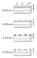
- Figure 5 illustrates the tenth example of this invention.
- the polymer obtained in Example 8 was coated as a bottom layer film and baked at 200 ° C for 30 minutes to form polymer organic film 41.
- SOG 42 was coated thereon and baked at 200 ° C for 20 minutes.
- polymethyl methacrylate (PMMA) was coated thereon as an electron beam resist 43 and baked at 170°C for 30 minutes ( Figure 5(a)).
- PMMA polymethyl methacrylate
- a positive or negative type of resist pattern having a high sensitivity and a high resolving power can be formed by using a polyalkylthiophene system, which is an electrically conductive organic polymeric substance, as an electron beam resist.
- a polyalkylthiophene system which is an electrically conductive organic polymeric substance
- vapor deposition for the formation of aluminum film is unnecessary, there is no problem of contamination, the process can be simplified, the charging-up phenomenon due to electron can be prevented, and an accurate fine pattern can be formed.
- a quaternary ammonium ion type polymer which is an ion conductive polymeric substance, is used as an electron beam resist, a resist pattern having a high sensitivity and a high resolving power can be formed.
Landscapes
- Chemical & Material Sciences (AREA)
- Physics & Mathematics (AREA)
- Engineering & Computer Science (AREA)
- Nanotechnology (AREA)
- General Physics & Mathematics (AREA)
- Polymers & Plastics (AREA)
- Crystallography & Structural Chemistry (AREA)
- Health & Medical Sciences (AREA)
- Chemical Kinetics & Catalysis (AREA)
- Medicinal Chemistry (AREA)
- Spectroscopy & Molecular Physics (AREA)
- Organic Chemistry (AREA)
- Theoretical Computer Science (AREA)
- Mathematical Physics (AREA)
- Composite Materials (AREA)
- Condensed Matter Physics & Semiconductors (AREA)
- Materials Engineering (AREA)
- Electron Beam Exposure (AREA)
Applications Claiming Priority (4)
| Application Number | Priority Date | Filing Date | Title |
|---|---|---|---|
| JP16164488A JP2586584B2 (ja) | 1988-06-29 | 1988-06-29 | 微細パターン形成方法 |
| JP161640/88 | 1988-06-29 | ||
| JP161644/88 | 1988-06-29 | ||
| JP63161640A JP2548308B2 (ja) | 1988-06-29 | 1988-06-29 | パターン形成方法 |
Related Parent Applications (2)
| Application Number | Title | Priority Date | Filing Date |
|---|---|---|---|
| EP89111823.4 Division | 1989-06-29 | ||
| EP89111823A Division EP0348961B1 (de) | 1988-06-29 | 1989-06-29 | Verfahren und Vorrichtung zur Herstellung von Feinstrukturen |
Publications (2)
| Publication Number | Publication Date |
|---|---|
| EP0530849A2 true EP0530849A2 (de) | 1993-03-10 |
| EP0530849A3 EP0530849A3 (de) | 1993-05-05 |
Family
ID=26487703
Family Applications (2)
| Application Number | Title | Priority Date | Filing Date |
|---|---|---|---|
| EP89111823A Expired - Lifetime EP0348961B1 (de) | 1988-06-29 | 1989-06-29 | Verfahren und Vorrichtung zur Herstellung von Feinstrukturen |
| EP19920116932 Withdrawn EP0530849A3 (de) | 1988-06-29 | 1989-06-29 | Verfahren und Vorrichtung zur Herstellung von Feinstrukturen |
Family Applications Before (1)
| Application Number | Title | Priority Date | Filing Date |
|---|---|---|---|
| EP89111823A Expired - Lifetime EP0348961B1 (de) | 1988-06-29 | 1989-06-29 | Verfahren und Vorrichtung zur Herstellung von Feinstrukturen |
Country Status (2)
| Country | Link |
|---|---|
| EP (2) | EP0348961B1 (de) |
| DE (1) | DE68912664T2 (de) |
Families Citing this family (4)
| Publication number | Priority date | Publication date | Assignee | Title |
|---|---|---|---|---|
| DE3903421A1 (de) * | 1989-02-06 | 1990-08-09 | Hoechst Ag | Elektrisch leitfaehige resistmasse, verfahren zu ihrer herstellung und ihre verwendung |
| JPH03261953A (ja) * | 1990-03-13 | 1991-11-21 | Fujitsu Ltd | 微細パターンの形成方法 |
| JPH04204848A (ja) * | 1990-11-30 | 1992-07-27 | Matsushita Electric Ind Co Ltd | 微細パターン形成方法 |
| US5512418A (en) * | 1993-03-10 | 1996-04-30 | E. I. Du Pont De Nemours And Company | Infra-red sensitive aqueous wash-off photoimaging element |
Family Cites Families (2)
| Publication number | Priority date | Publication date | Assignee | Title |
|---|---|---|---|---|
| US3658518A (en) * | 1969-04-04 | 1972-04-25 | Addressograph Multigraph | Three-layered reflex electrophotographic recording element |
| US4266004A (en) * | 1976-12-30 | 1981-05-05 | Monsanto Company | Photoimageable material of polymeric material having organic sulfide and photo-oxidation sensitizer |
-
1989
- 1989-06-29 EP EP89111823A patent/EP0348961B1/de not_active Expired - Lifetime
- 1989-06-29 EP EP19920116932 patent/EP0530849A3/de not_active Withdrawn
- 1989-06-29 DE DE68912664T patent/DE68912664T2/de not_active Expired - Fee Related
Also Published As
| Publication number | Publication date |
|---|---|
| DE68912664T2 (de) | 1994-08-18 |
| EP0348961B1 (de) | 1994-01-26 |
| EP0530849A3 (de) | 1993-05-05 |
| DE68912664D1 (de) | 1994-03-10 |
| EP0348961A2 (de) | 1990-01-03 |
| EP0348961A3 (de) | 1991-07-17 |
Similar Documents
| Publication | Publication Date | Title |
|---|---|---|
| EP0459255B1 (de) | Verfahren um das elektrische Aufladen zu vermeiden | |
| Lai | Polymers for electronic applications | |
| US5169494A (en) | Fine pattern forming method | |
| US5527662A (en) | Process for forming fine pattern | |
| Hatzakis | Electron resists for microcircuit and mask production | |
| US5314772A (en) | High resolution, multi-layer resist for microlithography and method therefor | |
| JP3349843B2 (ja) | 電離放射線照射用組成物及び電離放射線照射方法 | |
| EP0477035B1 (de) | Verfahren zur Herstellung einer Phasenverschiebungs-Photomaske | |
| US3934057A (en) | High sensitivity positive resist layers and mask formation process | |
| JPH06287454A (ja) | 水溶性で導電性の合成物質、生成方法および利用方法 | |
| CN101384963A (zh) | 一种使薄膜形成图案的方法 | |
| WO2002101463A1 (en) | Patterning compositions using e-beam lithography and structures and devices made thereby | |
| JPH02103547A (ja) | 導電性層の形成方法 | |
| US5306601A (en) | Fine pattern forming material and pattern forming method | |
| US5153103A (en) | Resist composition and pattern formation process | |
| EP0530849A2 (de) | Verfahren und Vorrichtung zur Herstellung von Feinstrukturen | |
| EP0390038B1 (de) | Feinmusterherstellungsverfahren | |
| KR100418739B1 (ko) | 조절된피에이치를갖는전기전도성중합체를포함하는조성물,상기전기전도성중합체의층을포함하는레지스트구조물,이구조물의제조방법 | |
| US5252430A (en) | Fine pattern forming method | |
| US5994007A (en) | Pattern forming method utilizing first insulative and then conductive overlayer and underlayer | |
| JP2548308B2 (ja) | パターン形成方法 | |
| JP2506952B2 (ja) | 微細パタ―ン形成方法 | |
| US4581318A (en) | N-alkynyl polyvinylpyridinium resists having electron and deep U.V. sensitivity | |
| KR101250190B1 (ko) | 포토레지스트 패턴 축소용 수용성 중합체, 상기 수용성중합체를 포함하는 포토레지스트 패턴 축소용 조성물 및 상기 조성물을 이용한 미세패턴 형성 방법 | |
| JPH06192440A (ja) | 導電性有機薄膜 |
Legal Events
| Date | Code | Title | Description |
|---|---|---|---|
| PUAI | Public reference made under article 153(3) epc to a published international application that has entered the european phase |
Free format text: ORIGINAL CODE: 0009012 |
|
| AC | Divisional application: reference to earlier application |
Ref document number: 348961 Country of ref document: EP |
|
| AK | Designated contracting states |
Kind code of ref document: A2 Designated state(s): DE FR GB |
|
| PUAL | Search report despatched |
Free format text: ORIGINAL CODE: 0009013 |
|
| AK | Designated contracting states |
Kind code of ref document: A3 Designated state(s): DE FR GB |
|
| 17P | Request for examination filed |
Effective date: 19930607 |
|
| 17Q | First examination report despatched |
Effective date: 19970115 |
|
| 18W | Application withdrawn |
Withdrawal date: 19980525 |