EP0532041A1 - Dispositif de mémoire statique de grande stabilité avec transistors à effet de champ à semi-conducteurs d'oxyde métallique - Google Patents
Dispositif de mémoire statique de grande stabilité avec transistors à effet de champ à semi-conducteurs d'oxyde métallique Download PDFInfo
- Publication number
- EP0532041A1 EP0532041A1 EP92115604A EP92115604A EP0532041A1 EP 0532041 A1 EP0532041 A1 EP 0532041A1 EP 92115604 A EP92115604 A EP 92115604A EP 92115604 A EP92115604 A EP 92115604A EP 0532041 A1 EP0532041 A1 EP 0532041A1
- Authority
- EP
- European Patent Office
- Prior art keywords
- mosfets
- driver
- access
- mosfet
- gate
- Prior art date
- Legal status (The legal status is an assumption and is not a legal conclusion. Google has not performed a legal analysis and makes no representation as to the accuracy of the status listed.)
- Granted
Links
Images



Classifications
-
- H—ELECTRICITY
- H10—SEMICONDUCTOR DEVICES; ELECTRIC SOLID-STATE DEVICES NOT OTHERWISE PROVIDED FOR
- H10B—ELECTRONIC MEMORY DEVICES
- H10B10/00—Static random access memory [SRAM] devices
- H10B10/15—Static random access memory [SRAM] devices comprising a resistor load element
-
- H—ELECTRICITY
- H10—SEMICONDUCTOR DEVICES; ELECTRIC SOLID-STATE DEVICES NOT OTHERWISE PROVIDED FOR
- H10D—INORGANIC ELECTRIC SEMICONDUCTOR DEVICES
- H10D84/00—Integrated devices formed in or on semiconductor substrates that comprise only semiconducting layers, e.g. on Si wafers or on GaAs-on-Si wafers
- H10D84/01—Manufacture or treatment
- H10D84/0123—Integrating together multiple components covered by H10D12/00 or H10D30/00, e.g. integrating multiple IGBTs
- H10D84/0126—Integrating together multiple components covered by H10D12/00 or H10D30/00, e.g. integrating multiple IGBTs the components including insulated gates, e.g. IGFETs
- H10D84/013—Manufacturing their source or drain regions, e.g. silicided source or drain regions
-
- H—ELECTRICITY
- H10—SEMICONDUCTOR DEVICES; ELECTRIC SOLID-STATE DEVICES NOT OTHERWISE PROVIDED FOR
- H10D—INORGANIC ELECTRIC SEMICONDUCTOR DEVICES
- H10D84/00—Integrated devices formed in or on semiconductor substrates that comprise only semiconducting layers, e.g. on Si wafers or on GaAs-on-Si wafers
- H10D84/01—Manufacture or treatment
- H10D84/0123—Integrating together multiple components covered by H10D12/00 or H10D30/00, e.g. integrating multiple IGBTs
- H10D84/0126—Integrating together multiple components covered by H10D12/00 or H10D30/00, e.g. integrating multiple IGBTs the components including insulated gates, e.g. IGFETs
- H10D84/0135—Manufacturing their gate conductors
- H10D84/0142—Manufacturing their gate conductors the gate conductors having different shapes or dimensions
-
- H—ELECTRICITY
- H10—SEMICONDUCTOR DEVICES; ELECTRIC SOLID-STATE DEVICES NOT OTHERWISE PROVIDED FOR
- H10D—INORGANIC ELECTRIC SEMICONDUCTOR DEVICES
- H10D84/00—Integrated devices formed in or on semiconductor substrates that comprise only semiconducting layers, e.g. on Si wafers or on GaAs-on-Si wafers
- H10D84/01—Manufacture or treatment
- H10D84/0123—Integrating together multiple components covered by H10D12/00 or H10D30/00, e.g. integrating multiple IGBTs
- H10D84/0126—Integrating together multiple components covered by H10D12/00 or H10D30/00, e.g. integrating multiple IGBTs the components including insulated gates, e.g. IGFETs
- H10D84/0144—Manufacturing their gate insulating layers
-
- Y—GENERAL TAGGING OF NEW TECHNOLOGICAL DEVELOPMENTS; GENERAL TAGGING OF CROSS-SECTIONAL TECHNOLOGIES SPANNING OVER SEVERAL SECTIONS OF THE IPC; TECHNICAL SUBJECTS COVERED BY FORMER USPC CROSS-REFERENCE ART COLLECTIONS [XRACs] AND DIGESTS
- Y10—TECHNICAL SUBJECTS COVERED BY FORMER USPC
- Y10S—TECHNICAL SUBJECTS COVERED BY FORMER USPC CROSS-REFERENCE ART COLLECTIONS [XRACs] AND DIGESTS
- Y10S257/00—Active solid-state devices, e.g. transistors, solid-state diodes
- Y10S257/903—FET configuration adapted for use as static memory cell
- Y10S257/904—FET configuration adapted for use as static memory cell with passive components,, e.g. polysilicon resistors
Definitions
- the present invention relates to a static memory device, and more particularly to a high stability static memory device having metal-oxide-semiconductor field-effect transistors (hereinafter referred to as "MOSFETs").
- MOSFETs metal-oxide-semiconductor field-effect transistors
- Fig. 1 shows a bit line load circuit and a memory cell circuit for a typical static memory device.
- D, D ⁇ denote a pair of bit lines
- W denotes a word line
- Q1, Q2 denote driver MOSFETs of inverters constituting a flip-flop for the memory
- Q3, Q4 denote access MOSFETs for connecting the memory cell with the bit lines D, D ⁇
- R1 and R2 denote load resistors of the inverters of the flip-flop for the memory
- Q5, Q6 denote load MOSFETs of the bit lines D, D ⁇ .
- the MOSFETs constituting the memory cell are all N-channel MOSFETs and the load MOSFETs of the bit lines are both P-channel MOSFETs.
- the data to be written are sent to the bit lines from a write circuit (omitted in Fig. 1) and one of the bit lines becomes a V CC level and the other becomes approximately a GND level.
- a write circuit (omitted in Fig. 1)
- one of the bit lines becomes a V CC level and the other becomes approximately a GND level.
- the word line W is caused to be in a selecting state (the V CC level) with the bit line D being made approximately the GND level and the bit line D being made the V CC level.
- the level of the node A which is H-level will be discharged through the access MOSFET Q3 so that the level of the node A will be turned to the L-level. Consequently, the driver MOSFET Q2 will be OFF, and the H-level of the bit line D ⁇ enters into the node B through the other access MOSFET Q4. In this manner, the opposite level data with respect to the initial data can be written in the memory cell.
- the H-level of the memory cell is at a voltage lower than the V CC by a threshold voltage V T of the access MOSFET.
- V T threshold voltage
- the word line W becomes the L-level and the memory cell is then in a holding state.
- both the access MOSFETs Q3 and Q4 are OFF, the driver MOSFET Q1 is ON and the driver MOSFET Q2 is OFF.
- Each of the load resistors R1 and R2 of the cell used has a high resistance value of above 100 G ⁇ so that the L-level of the memory cell becomes approximately the GND level.
- the H-level of the memory cell is at a voltage lower than the V CC by the threshold voltage V T of the access MOSFET immediately after the writing of the data as already explained, there develops a gradual charging through the cell load resistor, so that the H-level of the memory cell eventually reaches the V CC level.
- the L- and H-levels of the cell are the GND level and the V CC level, respectively.
- the word line is selected normally in a state in which the bit lines have precharged. That is, before the word line becomes the H-level, the potential of the bit lines D, D ⁇ has already become the V CC level. Therefore, when the level of the word line gradually rises, first the access MOSFET connected to the node at the L-level side of the memory cell becomes ON and, thus, the potential of the L-level of the memory cell starts to rise. However, under the normal state, this level is lowered by the driver MOSFET in an ON-state, followed by the lowering of the level of the word line in a precharged state down to the neighborhood of the GND level. On the other hand, the bit line at the node of the H-level side remains at a precharged state without being discharged to the L-level. That is, the data held by the memory cell has been thus read-out to the bit lines.
- an important factor for determining the stability of the memory cell is the degree as to how high the L-level at the L-level side node rises. If the L-level exceeds a threshold voltage of the driver MOSFET, the H-level of the memory cell abruptly drops from the V CC level to a voltage lower by the threshold voltage of the access MOSFET than the voltage of the word line. This results in the reduction of a potential difference between the H-level and the L-level of the memory cell and, in an actual memory cell, there is a risk in which the H-level and the L-level of the memory cell is reversed. In order to prevent the levels of the memory cell from being reversed, it is necessary to limit the rising of the L-level of the memory cell (which means that the rising of the L-level of the memory cell be limited so as not to exceed the threshold voltage of the driver MOSFET).
- Fig. 2 is an equivalent circuit diagram showing a portion of the circuit shown in Fig. 1.
- a transistor Q30 in Fig. 2 corresponds to the load transistors Q5, Q6 of Fig. 1; a transistor Q20 in Fig. 2 corresponds to the transistors Q3, Q4 of Fig. 1; a transistor Q10 in Fig. 2 corresponds to the driver transistors Q1, Q2 of Fig. 1; and a resistor R in Fig. 2 corresponds to the load resistors R1, R2 of Fig. 10, respectively.
- the circuit of Fig. 2 can be considered as an inverter circuit which is constituted by the transistor Q10 used as a driver MOSFET and a parallel circuit of the two MOSFETs Q20 and Q30 connected in series and the resistor R used as a load element. Input/output characteristics of such inverter are shown in Fig. 3. Fig.
- cell ratio the ratios between the current supply capability of the transistor Q10 and that of the transistor Q20 (generally and simply referred to as "cell ratio") are used as parameters, and this shows that the current supply capability of the transistor Q10 is two times, three times and four times greater than that of the transistor Q20. It can be appreciated from this that the greater the cell ratio is, the lower are the output voltages with respect to the same input voltage.
- the gain coefficient ⁇ is used as a constant for expressing the current supply capability of the MOSFETs.
- the means for making the cell ratio large has been to increase the aspect ratio (W/L) of the driver MOSFET and to decrease that of the access MOSFET.
- the gate width of the driver MOSFET is made large and the gate length thereof is made short while the gate width of the access MOSFET is made small and the gate length thereof is made long.
- a static memory device having a plurality of memory cells each comprising a pair of driver MOSFETs whose gates and drains are cross-connected; two load elements each of which is connected between a power source and the drain of each of the driver MOSFETs; and two access MOSFETs each of which is connected between the drain of each of the driver MOSFETs and each of a pair of bit lines and whose gates are connected to a word line
- the static memory device is characterized in that, a width/length aspect ratio of each gate of the driver MOSFETs is greater than that of each gate of the access MOSFETs; and a ratio between a gain coefficient of each of the driver MOSFETs and a gain coefficient of each of the access MOSFETs is greater than a ratio between the aspect ratio of each gate of the driver MOSFETs and the aspect ratio of each gate of the access MOSFETs.
- the gain coefficient ratio between the driver MOSFETs and the access MOSFETs larger than the ratio of the width/length aspect ratios of these transistors
- various means which include, for example, (1) a means wherein the thickness of a gate oxide film of each of the access MOSFETs is made thicker than that of each of the driver MOSFETs; (2) means wherein each of the transistors is made in an LDD (Lightly Doped Drain) configuration or a DDD (Double Diffused Drain) configuration and an impurity concentration of the low impurity concentration regions of the access MOSFETs is made lower than that of the low impurity concentration regions of the driver MOSFETs; and (3) a means wherein either or both of the source/drain regions of the access MOSFETs have an impurity concentration lower than that in the source/drain regions of the driver MOSFETs.
- LDD Lightly Doped Drain
- DDD Double Diffused Drain
- Fig. 4 is a sectional view showing a cell structure of a first embodiment according to the invention.
- the structure shown in Fig. 4 includes a p-well 1; a field oxide film 2; a gate oxide film 3a and a gate electrode 4a of a driver MOSFET; a gate oxide film 3b and a gate electrode 4b of an access MOSFET; and an n+-type diffusion layer 5 constituting a source/drain region.
- the thickness of the gate oxide film 3b of the access MOSFET in this embodiment is made thicker than that of the gate oxide film 3a of the driver MOSFET.
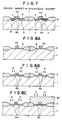
- a method of fabricating the cell structure of the first embodiment according to the invention is explained with reference to Figs. 5A through 5D.
- Fig. 5A by the ordinary methods, the necessary field oxide films 2 for device isolation are formed on the p-well 1.
- Fig. 5B a gate oxide film precursor 3c with a thickness of 70 ⁇ is formed on an entire surface by means of a thermal oxidation method.
- a layer of photoresist 8a is applied on the gate oxide film precursor 3c, and the oxide film is etched away after the layer of photoresist at the portion of the access MOSFET is kept remained.
- the photoresist 8a is removed and again the thermal oxidation is performed thereby causing an oxide film with the necessary thickness of (180 ⁇ ) of the gate oxide film of the driver MOSFET to grow and then a gate oxide film 3a is formed as shown in Fig. 5D. Consequently, the thickness of the gate oxide film 3b of the access MOSFET is the sum 250 ⁇ of the thickness 70 ⁇ of the gate oxide film precursor 3c and the thickness 180 ⁇ of the gate oxide film 3a of the driver MOSFET.
- a film of polysilicon is deposited on the resultant surface. This film is patterned and the gate electrodes 4a, 4b are formed and, thereafter, a device as shown in Fig. 4 is formed after ion-implantation and thermal oxidation processes are conducted.
- Fig. 6 is a graph which shows how the process gain coefficient K as an index of the capability of the MOSFET relates to the thicknesses of the gate oxide film and in which the gate oxide film thicknesses are given in the axis of abscissas and the process gain coefficient is given in the axis of ordinates.
- the thickness of the gate oxide film 3a of the driver MOSFET is 180 ⁇ and that of the gate oxide film 3b of the access MOSFET is 250 ⁇ , so that the process gain coefficient of the driver MOSFET is approximately 320 ⁇ S (micro siemens)/V and that of the access MOSFET is approximately 240 ⁇ S/V.
- Fig. 7 is a sectional view showing a structure of a second embodiment according to the present invention.
- the structure shown is a MOSFET of a lightly doped drain (hereinafter referred to as "LDD") structure which has been developed with the attention being paid to the fact that, as unique characteristics to the LDD structure, the current supply capability varies depending on the impurity concentration of the low impurity concentration region.
- LDD lightly doped drain
- the impurity concentration of the low impurity concentration diffusion layer of the access MOSFET is made lower than the impurity concentration of the low impurity concentration diffusion layer of the driver MOSFET and in this way the ratio is made large.
- the structure shown in Fig. 7 includes a p-well 1; a field oxide film 2; a gate oxide film 3; a gate electrode 4a of the driver MOSFET; a gate electrode 4b of the access M0SFET; an n+-type diffusion layer 5; an n ⁇ -type diffusion layer 6a; an n ⁇ -type diffusion layer 6b, and a side wall 7.
- the fabrication up to the formation of the gate electrodes 4a and 4b follows the same procedure as in the conventional fabrication method (See Fig. 8A). Then, with the gate electrodes used as masks, the entire surface is subjected to the ion-implantation in a dose of 1 ⁇ 1013/cm2, so that the n ⁇ type diffusion layers 6b are formed and so that the impurity concentration thereof becomes that required to the low impurity concentration diffusion layer of the access MOSFET (See Fig. 8B).
- the n ⁇ -type diffusion layers 6a are formed by the ion-implantation in a dose of 2 ⁇ 1013/cm2 so as to be in the low impurity concentration of the driver MOSFET.
- the dose to the n ⁇ -type diffusion layer 6a will be 3 ⁇ 1013/cm2.
- the side wall 7 is formed after the removal of the photoresist 8a and the n+-type diffusion layer 5 is formed by the ion-implantation of high impurity concentration, whereby the device as shown in Fig. 7 is obtained.
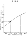
- Fig. 9 is a graph showing the relation which the current supply capability of the MOSFET having the LDD structure has with the impurity concentration of the low impurity concentration diffusion layer.
- the amount of impurity ion-implantation into the low impurity concentration diffusion layer is given in the axis of abscissas and the process gain coefficient K is given in the axis of ordinates.
- the dose of ion-implantation to the n ⁇ -type diffusion layer 6a of the driver MOSFET is 3 ⁇ 1013/cm2 and the dose of ion-implantation to the n ⁇ -type diffusion layer 6b of the access MOSFET is 1 ⁇ 1013/cm2, so that the process gain coefficient K of the driver MOSFET will be 347 ⁇ S/V and that of the access MOSFET will be 220 ⁇ S/V.
- Fig. 10C shows is a sectional view showing a cell structure according to a third embodiment of the invention, and Figs. 10A and 10B show sectional views of the structure for illustrating the fabrication steps therefor.
- Fig. 10A after the gate oxide film 3 is partly removed, polycrystalline silicon is deposited followed by the doping of impurities and the patterning, whereby there are formed the gate electrode 4b of the access MOSFET and a polycrystalline silicon interconnect 4 which is connected to the gate electrode of the driver MOSFET (not shown) and one end of which is in contact with the n-type diffusion layer 9 on the substrate.
- the photoresist 8b is formed followed by the ion-implantation of arsenic (As) at an accelerating energy of 50 keV and in a dose of 5 ⁇ 1015/cm2, whereby an n+-type diffusion layers 5 which serve as a source/drain region at the bit line side of the access MOSFET and a source/drain region (not shown) of the driver MOSFET are formed.
- As arsenic
- an interlayer insulating film 10 is formed and, after the formation of a contact hole therein, polysilicon interconnects 11 connecting high resistance elements and memory node portions are formed, and also an interlayer insulating film 12 and an aluminum (Al) interconnect 13 constituting a bit line are formed.
- the impurity concentrations of the n-type diffusion layer 9, the n+-type diffusion layer 5 and the n ⁇ -type diffusion layer 6a are A, B and C, respectively, their relation is B»A ⁇ C.
- the impurity concentration of the source/drain region at the memory node side of the access MOSFET is lowered thereby lowering the current supply capability of this transistor.
- the impurity concentration at this region is lowered excessively, the cell ratio may become better but the resistance value becomes high causing the lowering of a speed for data writing, which means that there is a limit in the lowering of the impurity concentration.
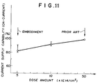
- Fig. 11 As shown in Fig. 11, when the dose of ion-implantation to one of the source/drain regions of the access MOSFET is lowered from 5 ⁇ 1015/cm2 to 5 ⁇ 1014/cm2, the current supply capability of the access MOSFET is lowered to 84%.
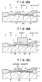
- Fig. 12C is a sectional view showing a cell structure of a fourth embodiment according to the invention, and Figs. 12A and 12B show in sectional views the structure illustrating the fabrication steps therefor.
- This embodiment relates to an example in which the bit line side source/drain region of the access MOSFET and the source/drain region of the driver MOSFET are formed in the LDD configuration.
- a gate electrode 4b of the access MOSFET and a polycrystalline silicon interconnect 4 connected to the gate electrode of the driver MOSFET are formed and, thereafter, an n ⁇ -type diffusion layer 6a is formed by the ion-implantation of phosphorus (P) at an accelerating energy of 35 keV and in a dose of 3 ⁇ 1013/cm2.
- P phosphorus
- a side wall 7 is formed on each side wall portion of the gate electrode 4b and of the gate electrode of the driver MOSFET which is not shown in the drawings, and a photoresist 8b is formed on the source/drain region at the memory node side thereof.
- arsenic (As) is ion-implanted at an accelerating energy of 50 keV and in a dose of 5 ⁇ 1015/cm2, whereby an n+-type diffusion layer 5 is formed as a source/drain region at the bit line side of the access MOSFET and a source/drain region of the driver MOSFET as shown in Fig. 12B.
- the photoresist 8b is removed as shown in Fig. 12C.
- the first embodiment may be modified by using a nitride film for the gate insulating film of the driver MOSFET while keeping the gate insulating film of the access MOSFET as the oxide film (in which case the thicknesses of the gate insulating films of the two transistors can be made approximately the same).
- the second embodiment may be modified by adopting a double diffusion drain structure (the so-called "DDD" structure) in place of the MOSFET of the LDD structure.
- DDD double diffusion drain structure
- the source/drain region at the bit line side be formed by an n ⁇ -type diffusion layer (with the memory node side being made an n+-type diffusion layer), or it is possible to lower the impurity concentrations of the source/drain regions of both the bit line side and the memory node side (in which case the source/drain region at one side is formed by the region whose impurity concentration is higher than the impurity concentration of the source/drain region at the other side that is formed by the low impurity concentration region).
- the fourth embodiment may also be modified so as to make the impurity concentration of the n ⁇ -type diffusion layer of the LDD structure at the bit line side different from that of the n ⁇ -type diffusion layer serving as the source/drain region at the memory node side.
- the consideration is given as to the influence that the above modification to the fourth embodiment has with respect to hot-carrier degradation or suppressing effects.
- the diffusion layers having the same concentration are provided respectively at both the sides of the source/drain region with the impurity concentration of the n ⁇ -type diffusion layer being an optimum concentration determined by the device dimensions.
- the impurity concentration of the n ⁇ -type diffusion layer at the bit line side is determined with a view to cope with hot carriers as mentioned above, and the impurity concentration of the source/drain region at the memory node side is determined by taking into account the operation stability and the operation speeds of the memory cell.
- both the bit lines are caused to be H-level, so that the bit line sides become drains in both the access MOSFETs.
- the structure since the drains are in the LDD configuration, the structure may be considered the same as that of the prior art in consideration of the hot carriers.
- the bit line sides become drains so that the same applies here as in the above read-out mode and, where the memory node sides become drains on the contrary, the current which flows to the access MOSFET is the charge accumulated in the capacitance at the memory node side, so that hot carriers have almost no effect. Therefore, even where the above modification is applied to a miniaturized or scaled-down structure, the impurity concentration of the source/drain at the memory node side can be determined irrespective of the concentration normally taken into account for coping with hot carriers.
- the cell ratio of the memory cell is made greater than the ratio of the aspect ratios of the driver MOSFET and the access MOSFET and, as a result, it has been made possible to enhance the stability of the memory cell without the need of increasing the chip size and without sacrificing the fabrication and operational tolerances.
- the threshold voltage V T of the access MOSFET is virtually without change from that in the conventional structure. This has a significant bearing on the operational stability from another aspect.
- the threshold voltage V T becomes high to a large extent.
- the H-level of the memory cell immediately after the writing is lowered so that, if the read-out takes place without the lapse of a sufficient time after the writing, there is a risk of the data inversion of the memory cell.
- the present invention since the current supply capability is lowered with the threshold value remaining almost the same as that in the prior art, the problem such as the inversion of the memory cell does not occur.
Landscapes
- Semiconductor Memories (AREA)
- Metal-Oxide And Bipolar Metal-Oxide Semiconductor Integrated Circuits (AREA)
Applications Claiming Priority (2)
| Application Number | Priority Date | Filing Date | Title |
|---|---|---|---|
| JP3262842A JP2754977B2 (ja) | 1991-02-08 | 1991-09-13 | スタティックメモリ |
| JP262842/91 | 1991-09-13 |
Publications (2)
| Publication Number | Publication Date |
|---|---|
| EP0532041A1 true EP0532041A1 (fr) | 1993-03-17 |
| EP0532041B1 EP0532041B1 (fr) | 1997-01-15 |
Family
ID=17381377
Family Applications (1)
| Application Number | Title | Priority Date | Filing Date |
|---|---|---|---|
| EP92115604A Expired - Lifetime EP0532041B1 (fr) | 1991-09-13 | 1992-09-11 | Dispositif de mémoire statique de grande stabilité avec transistors à effet de champ à semi-conducteurs d'oxyde métallique |
Country Status (4)
| Country | Link |
|---|---|
| US (1) | US5285096A (fr) |
| EP (1) | EP0532041B1 (fr) |
| KR (1) | KR970007589B1 (fr) |
| DE (1) | DE69216728T2 (fr) |
Families Citing this family (21)
| Publication number | Priority date | Publication date | Assignee | Title |
|---|---|---|---|---|
| US5825070A (en) * | 1993-11-30 | 1998-10-20 | Stmicroelectronics, Inc. | Structure for transistor devices in an SRAM cell |
| JPH0878533A (ja) * | 1994-08-31 | 1996-03-22 | Nec Corp | 半導体装置及びその製造方法 |
| US5703392A (en) * | 1995-06-02 | 1997-12-30 | Utron Technology Inc | Minimum size integrated circuit static memory cell |
| JPH09312399A (ja) * | 1995-07-14 | 1997-12-02 | Seiko Instr Inc | 半導体装置とその製造方法 |
| KR0186070B1 (ko) * | 1995-12-28 | 1999-03-20 | 문정환 | 반도체 메모리 구조 및 그 제조방법 |
| US5691217A (en) * | 1996-01-03 | 1997-11-25 | Micron Technology, Inc. | Semiconductor processing method of forming a pair of field effect transistors having different thickness gate dielectric layers |
| KR100277878B1 (ko) * | 1996-11-08 | 2001-02-01 | 김영환 | 트랜지스터의 구조 및 제조방법 |
| JPH10223771A (ja) * | 1997-02-12 | 1998-08-21 | Yamaha Corp | 半導体装置とその製造方法 |
| US5939762A (en) * | 1997-06-26 | 1999-08-17 | Integrated Device Technology, Inc. | SRAM cell using thin gate oxide pulldown transistors |
| JP3967440B2 (ja) * | 1997-12-09 | 2007-08-29 | 株式会社ルネサステクノロジ | 半導体集積回路装置の製造方法 |
| JP4931267B2 (ja) | 1998-01-29 | 2012-05-16 | ルネサスエレクトロニクス株式会社 | 半導体装置 |
| JP3467416B2 (ja) * | 1998-04-20 | 2003-11-17 | Necエレクトロニクス株式会社 | 半導体記憶装置及びその製造方法 |
| TW375836B (en) * | 1998-05-04 | 1999-12-01 | United Microelectronics Corp | SRAM (static random access memory) manufacturing method |
| US6165918A (en) * | 1999-05-06 | 2000-12-26 | Integrated Device Technology, Inc. | Method for forming gate oxides of different thicknesses |
| JP2001068564A (ja) * | 1999-08-30 | 2001-03-16 | Mitsubishi Electric Corp | 半導体装置およびその製造方法 |
| JP2001203347A (ja) | 2000-01-18 | 2001-07-27 | Mitsubishi Electric Corp | 半導体装置およびその製造方法 |
| JP2001210718A (ja) * | 2000-01-26 | 2001-08-03 | Nec Corp | 半導体集積回路及びその設計方法 |
| JP2002016150A (ja) * | 2000-06-29 | 2002-01-18 | Nec Corp | 半導体記憶装置及びその製造方法 |
| JP4592193B2 (ja) * | 2001-02-06 | 2010-12-01 | ルネサスエレクトロニクス株式会社 | 半導体装置の製造方法 |
| US7189662B2 (en) * | 2004-08-24 | 2007-03-13 | Micron Technology, Inc. | Methods of forming semiconductor constructions |
| DE102008035805B4 (de) * | 2008-07-31 | 2013-01-31 | Advanced Micro Devices, Inc. | Herstellung von Gatedielektrika in PMOS- und NMOS-Transistoren |
Citations (3)
| Publication number | Priority date | Publication date | Assignee | Title |
|---|---|---|---|---|
| US4443715A (en) * | 1982-03-25 | 1984-04-17 | Gte Laboratories Incorporated | Driver circuit |
| GB2238437A (en) * | 1989-11-22 | 1991-05-29 | Plessey Co Plc | Transistor driver circuits |
| EP0435457A1 (fr) * | 1989-11-24 | 1991-07-03 | Sharp Kabushiki Kaisha | Dispositif de mémoire semi-conductrice et préparation associée |
Family Cites Families (3)
| Publication number | Priority date | Publication date | Assignee | Title |
|---|---|---|---|---|
| US4866002A (en) * | 1985-11-26 | 1989-09-12 | Fuji Photo Film Co., Ltd. | Complementary insulated-gate field effect transistor integrated circuit and manufacturing method thereof |
| US4890144A (en) * | 1987-09-14 | 1989-12-26 | Motorola, Inc. | Integrated circuit trench cell |
| JPH0513714A (ja) * | 1990-01-25 | 1993-01-22 | Texas Instr Inc <Ti> | 溝型トランジスタ使用の双安定論理デバイス |
-
1992
- 1992-09-09 KR KR1019920016528A patent/KR970007589B1/ko not_active Expired - Fee Related
- 1992-09-11 US US07/944,117 patent/US5285096A/en not_active Expired - Lifetime
- 1992-09-11 EP EP92115604A patent/EP0532041B1/fr not_active Expired - Lifetime
- 1992-09-11 DE DE69216728T patent/DE69216728T2/de not_active Expired - Fee Related
Patent Citations (3)
| Publication number | Priority date | Publication date | Assignee | Title |
|---|---|---|---|---|
| US4443715A (en) * | 1982-03-25 | 1984-04-17 | Gte Laboratories Incorporated | Driver circuit |
| GB2238437A (en) * | 1989-11-22 | 1991-05-29 | Plessey Co Plc | Transistor driver circuits |
| EP0435457A1 (fr) * | 1989-11-24 | 1991-07-03 | Sharp Kabushiki Kaisha | Dispositif de mémoire semi-conductrice et préparation associée |
Also Published As
| Publication number | Publication date |
|---|---|
| US5285096A (en) | 1994-02-08 |
| KR970007589B1 (ko) | 1997-05-10 |
| KR930006950A (ko) | 1993-04-22 |
| DE69216728T2 (de) | 1997-08-07 |
| EP0532041B1 (fr) | 1997-01-15 |
| DE69216728D1 (de) | 1997-02-27 |
Similar Documents
| Publication | Publication Date | Title |
|---|---|---|
| EP0532041B1 (fr) | Dispositif de mémoire statique de grande stabilité avec transistors à effet de champ à semi-conducteurs d'oxyde métallique | |
| US4495693A (en) | Method of integrating MOS devices of double and single gate structure | |
| US7981738B2 (en) | Semiconductor memory device and a method of manufacturing the same | |
| US5266507A (en) | Method of fabricating an offset dual gate thin film field effect transistor | |
| US6228704B1 (en) | Process for manufacturing semiconductor integrated circuit device | |
| KR100214841B1 (ko) | 반도체 소자 및 그의 제조방법 | |
| KR100221439B1 (ko) | 반도체 메모리 | |
| JPH0837243A (ja) | Sramメモリセル及び半導体回路 | |
| EP0392540B1 (fr) | Mémoire statique | |
| EP0513644A2 (fr) | Transistor à effet de champ en couche mince et procédé sa fabrication | |
| US5377140A (en) | Cell for random access memory | |
| KR100282755B1 (ko) | 반도체 장치 | |
| KR0183485B1 (ko) | 반도체 디바이스 및 그 제조 방법 | |
| US6025253A (en) | Differential poly-edge oxidation for stable SRAM cells | |
| JP2005210052A (ja) | 半導体装置およびその製造方法 | |
| US6090654A (en) | Method for manufacturing a static random access memory cell | |
| EP0214561A2 (fr) | Mémoire RAM | |
| KR19980081724A (ko) | 구동 트랜지스터의 소오스에 인접한 포켓영역을 갖는스태틱 랜덤 억세스 메모리셀 | |
| JP2754977B2 (ja) | スタティックメモリ | |
| US20030218218A1 (en) | SRAM cell with reduced standby leakage current and method for forming the same | |
| JP2682411B2 (ja) | 半導体記憶装置 | |
| JPS61218165A (ja) | 半導体記憶装置及び製造方法 | |
| JPH06151773A (ja) | スタティック型半導体記憶装置およびその製造方法 | |
| JP3067678B2 (ja) | 半導体装置 | |
| EP0821413B1 (fr) | Cellules SRAM et méthode de fabrication |
Legal Events
| Date | Code | Title | Description |
|---|---|---|---|
| PUAI | Public reference made under article 153(3) epc to a published international application that has entered the european phase |
Free format text: ORIGINAL CODE: 0009012 |
|
| AK | Designated contracting states |
Kind code of ref document: A1 Designated state(s): DE FR GB NL |
|
| 17P | Request for examination filed |
Effective date: 19930122 |
|
| GRAG | Despatch of communication of intention to grant |
Free format text: ORIGINAL CODE: EPIDOS AGRA |
|
| GRAH | Despatch of communication of intention to grant a patent |
Free format text: ORIGINAL CODE: EPIDOS IGRA |
|
| 17Q | First examination report despatched |
Effective date: 19960619 |
|
| GRAH | Despatch of communication of intention to grant a patent |
Free format text: ORIGINAL CODE: EPIDOS IGRA |
|
| GRAA | (expected) grant |
Free format text: ORIGINAL CODE: 0009210 |
|
| AK | Designated contracting states |
Kind code of ref document: B1 Designated state(s): DE FR GB NL |
|
| REF | Corresponds to: |
Ref document number: 69216728 Country of ref document: DE Date of ref document: 19970227 |
|
| ET | Fr: translation filed | ||
| PLBE | No opposition filed within time limit |
Free format text: ORIGINAL CODE: 0009261 |
|
| 26N | No opposition filed | ||
| PGFP | Annual fee paid to national office [announced via postgrant information from national office to epo] |
Ref country code: FR Payment date: 20010911 Year of fee payment: 10 |
|
| PGFP | Annual fee paid to national office [announced via postgrant information from national office to epo] |
Ref country code: GB Payment date: 20010912 Year of fee payment: 10 |
|
| PGFP | Annual fee paid to national office [announced via postgrant information from national office to epo] |
Ref country code: DE Payment date: 20010924 Year of fee payment: 10 |
|
| PGFP | Annual fee paid to national office [announced via postgrant information from national office to epo] |
Ref country code: NL Payment date: 20010927 Year of fee payment: 10 |
|
| REG | Reference to a national code |
Ref country code: GB Ref legal event code: IF02 |
|
| PG25 | Lapsed in a contracting state [announced via postgrant information from national office to epo] |
Ref country code: GB Free format text: LAPSE BECAUSE OF NON-PAYMENT OF DUE FEES Effective date: 20020911 |
|
| PG25 | Lapsed in a contracting state [announced via postgrant information from national office to epo] |
Ref country code: NL Free format text: LAPSE BECAUSE OF NON-PAYMENT OF DUE FEES Effective date: 20030401 Ref country code: DE Free format text: LAPSE BECAUSE OF NON-PAYMENT OF DUE FEES Effective date: 20030401 |
|
| GBPC | Gb: european patent ceased through non-payment of renewal fee |
Effective date: 20020911 |
|
| PG25 | Lapsed in a contracting state [announced via postgrant information from national office to epo] |
Ref country code: FR Free format text: LAPSE BECAUSE OF NON-PAYMENT OF DUE FEES Effective date: 20030603 |
|
| REG | Reference to a national code |
Ref country code: FR Ref legal event code: ST |