EP0532164A2 - Générateur de signal parabolique - Google Patents
Générateur de signal parabolique Download PDFInfo
- Publication number
- EP0532164A2 EP0532164A2 EP92306317A EP92306317A EP0532164A2 EP 0532164 A2 EP0532164 A2 EP 0532164A2 EP 92306317 A EP92306317 A EP 92306317A EP 92306317 A EP92306317 A EP 92306317A EP 0532164 A2 EP0532164 A2 EP 0532164A2
- Authority
- EP
- European Patent Office
- Prior art keywords
- amplifier
- output
- absolute value
- circuit
- entered
- Prior art date
- Legal status (The legal status is an assumption and is not a legal conclusion. Google has not performed a legal analysis and makes no representation as to the accuracy of the status listed.)
- Ceased
Links
Images
Classifications
-
- H—ELECTRICITY
- H03—ELECTRONIC CIRCUITRY
- H03K—PULSE TECHNIQUE
- H03K4/00—Generating pulses having essentially a finite slope or stepped portions
- H03K4/04—Generating pulses having essentially a finite slope or stepped portions having parabolic shape
-
- H—ELECTRICITY
- H04—ELECTRIC COMMUNICATION TECHNIQUE
- H04N—PICTORIAL COMMUNICATION, e.g. TELEVISION
- H04N3/00—Scanning details of television systems; Combination thereof with generation of supply voltages
- H04N3/10—Scanning details of television systems; Combination thereof with generation of supply voltages by means not exclusively optical-mechanical
- H04N3/16—Scanning details of television systems; Combination thereof with generation of supply voltages by means not exclusively optical-mechanical by deflecting electron beam in cathode-ray tube, e.g. scanning corrections
Definitions
- This invention relates to a parabolic signal generator used with the deflection circuit and dynamic focusing circuit (will be termed "DAF" hereinafter) of television receivers and display apparatus.
- DAF dynamic focusing circuit
- CRT cathode ray tube
- DAF circuits are introduced so as to improve the peripheral focus characteristics of the CRT. This purpose is achieved by operating the DAF circuit to generate a parabolic waveform and applying the waveform to the focus terminal of the CRT.
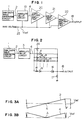
- Fig. 2 shows the conventional parabolic signal generator.
- symbol 1 denotes a saw-tooth wave generation circuit
- 3 is an absolute value circuit
- 5, 7, 10, 14, 17 and 24 are resistors
- 6, 8, 9, 11, 12, 13, 15 and 16 are diodes.
- the saw-tooth wave generation circuit 1 converts a current flowing in the deflection coil into a voltage shown in Fig. 3A
- the absolute value circuit 3 folds the saw-tooth waveform with respect to its center to produce a waveform shown in Fig. 3B
- a polygonal approximation circuit formed of the resistors 5, 7, 10, 14, 17 and 24 and the diodes 6, 8, 9, 11, 12, 13, 15 and 16 operates to make parallel connections of registers in response to the conduction of sets of diodes which are in serial connection with the respective resistors, so that a parabolic waveform is produced.
- the present invention is intended to solve the foregoing prior art deficiency, and its object is to provide a parabolic signal generator which realizes the expression (1) by means of a logarithmic amplifier, a linear amplifier and an antilogarithmic amplifier.
- the logarithmic amplifier needs to have an input voltage which is higher than its reference voltage because of the definition of logarithm in the range of positive real numbers, and on this account the absolute value circuit which precedes the logarithmic amplifier has its reference voltage made equal to that of the logarithmic amplifier so that the input of the logarithmic amplifier does not fall undefined.
- the inventive parabolic signal generator is designed to apply a sync pulse to a saw-tooth wave generation circuit, enter the output of the saw-tooth wave generation circuit to an absolute value circuit, enter the output of the absolute value circuit to a logarithmic amplifier, enter the output of the logarithmic amplifier to a linear amplifier, and enter the output of the linear amplifier to an antilogarithmic amplifier.
- the absolute value circuit, logarithmic amplifier, linear amplifier and antilogarithmic amplifier are powered by a single-voltage power source, and these circuit and amplifiers have their reference input terminals supplied with a common bias voltage.
- the parameter ⁇ of the expression (1) can be determined by setting the gain of the linear amplifier (generally, it is given as a ratio of resistances of two resistors), and when the ⁇ is determined as characteristics of CRT, the gain of the linear amplifier is simply set to ⁇ , and the input voltage to the logarithmic amplifier is guarantied to be higher than the reference voltage of the logarithmic amplifier.
- Fig. 1 denotes a saw-tooth wave generation circuit
- 2 is a saw-tooth wave signal
- 19 is an absolute value circuit which receives the saw-tooth wave signal
- 4 is an output signal of the absolute value circuit
- 20 is a linear amplifier which receives the output of the absolute value circuit
- 21 is a linear amplifier which receives the output of the logarithmic amplifier
- 22 is an antilogarithmic amplifier which receives the output of the linear amplifier
- 23 is a reference voltage input terminal
- 18 is an output terminal for the output which is expressed as Y in the expression (1) (in which ⁇ denotes the gain of the linear amplifier 21).
- the saw-tooth wave signal 2 shown in Fig. 3A is applied to the absolute value circuit 19, which then produces the output signal 4 shown in Fig. 3B.
- the reference voltage Vref is set to the level which crosses the center of the saw-tooth wave signal 2 as shown in Fig. 3A. Accordingly, point A in Figs. 3A and 3B does not fall below the reference voltage Vref, and thus it does not become an undefined voltage for the logarithmic amplifier 20 located in the following stage.
- the expression (1) is realized by the operations of the logarithmic amplifier 20, linear amplifier 21 and antilogarithmic amplifier 22 as follows.
- the output Y1 of the logarithmic amplifier 20, the output Y a of the linear amplifier 21, and the output Y0 of the antilogarithmic amplifier 22 are given as functions of the input voltage X as follows.
- the logarithmic amplifier does not have undefined regions through the provision of a common reference voltage for the absolute value circuit, logarithmic amplifier, linear amplifier and antilogarithmic amplifier.
- the parameter ⁇ of the expression (1) can be altered by setting the gain of the linear amplifier arbitrarily, whereby the signal generator can readily be modified when the CRT is switched to another type.
- the operation expressed by the expressions (1), (2), (3) and (4) produces accurate parabolic waveforms. Consequently, the parabolic waveform signal generator based on this invention can be designed efficiently, the circuit arrangement shown in Fig. 1 is suitable for circuit integration for cost reduction, and the influence of the thermal characteristics of diode on the waveform, which is encountered in the prior art circuit arrangement, can be eliminated according to this invention.
Landscapes
- Engineering & Computer Science (AREA)
- Multimedia (AREA)
- Signal Processing (AREA)
- Details Of Television Scanning (AREA)
Applications Claiming Priority (2)
| Application Number | Priority Date | Filing Date | Title |
|---|---|---|---|
| JP172537/91 | 1991-07-12 | ||
| JP17253791A JP3318932B2 (ja) | 1991-07-12 | 1991-07-12 | パラボラ信号発生装置 |
Publications (2)
| Publication Number | Publication Date |
|---|---|
| EP0532164A2 true EP0532164A2 (fr) | 1993-03-17 |
| EP0532164A3 EP0532164A3 (en) | 1994-07-20 |
Family
ID=15943737
Family Applications (1)
| Application Number | Title | Priority Date | Filing Date |
|---|---|---|---|
| EP19920306317 Ceased EP0532164A3 (en) | 1991-07-12 | 1992-07-09 | Parabolic signal generator |
Country Status (7)
| Country | Link |
|---|---|
| US (1) | US5223799A (fr) |
| EP (1) | EP0532164A3 (fr) |
| JP (1) | JP3318932B2 (fr) |
| KR (1) | KR960007262B1 (fr) |
| AU (1) | AU631509B1 (fr) |
| CA (1) | CA2073392C (fr) |
| TW (1) | TW241414B (fr) |
Families Citing this family (4)
| Publication number | Priority date | Publication date | Assignee | Title |
|---|---|---|---|---|
| JPH06339148A (ja) * | 1993-03-29 | 1994-12-06 | Hitachi Ltd | 色補正器、それを用いた画像表示装置、及び該画像表示装置から成る白バランス調整システム、並びに、白バランス調整方法、及び色調整方法 |
| CN101042977B (zh) | 2006-03-22 | 2011-12-21 | 清华大学 | 碳纳米管场发射电子源及其制造方法以及一场发射阵列 |
| CN100573783C (zh) | 2006-04-05 | 2009-12-23 | 清华大学 | 碳纳米管场发射电子源的制造方法 |
| CN106169912B (zh) * | 2016-06-28 | 2018-03-16 | 浙江中医药大学 | 脉冲波发生电路 |
Family Cites Families (6)
| Publication number | Priority date | Publication date | Assignee | Title |
|---|---|---|---|---|
| US3714505A (en) * | 1970-12-01 | 1973-01-30 | Bell Telephone Labor Inc | Dynamic focus correction apparatus for a rectilinearly raster scanned electron beam |
| JPS5928352A (ja) * | 1982-08-09 | 1984-02-15 | Hitachi Ltd | 位置決め装置 |
| US4849652A (en) * | 1986-12-01 | 1989-07-18 | U.S. Philips Corporation | Circuit for producing a periodic, essentially parabolic signal |
| JPH06101674B2 (ja) * | 1988-09-20 | 1994-12-12 | 三洋電機株式会社 | パラボラ波発生回路 |
| NL8901147A (nl) * | 1989-05-08 | 1990-12-03 | Philips Nv | Schakeling voor het leveren van een periodiek in wezen paraboolvormig signaal. |
| JP3182759B2 (ja) * | 1990-09-05 | 2001-07-03 | ソニー株式会社 | パラボラ波発生回路 |
-
1991
- 1991-07-12 JP JP17253791A patent/JP3318932B2/ja not_active Expired - Fee Related
-
1992
- 1992-07-07 US US07/909,706 patent/US5223799A/en not_active Expired - Fee Related
- 1992-07-08 CA CA002073392A patent/CA2073392C/fr not_active Expired - Fee Related
- 1992-07-09 TW TW081105432A patent/TW241414B/zh active
- 1992-07-09 EP EP19920306317 patent/EP0532164A3/en not_active Ceased
- 1992-07-09 AU AU19549/92A patent/AU631509B1/en not_active Ceased
- 1992-07-10 KR KR1019920012279A patent/KR960007262B1/ko not_active Expired - Fee Related
Also Published As
| Publication number | Publication date |
|---|---|
| CA2073392A1 (fr) | 1993-01-13 |
| EP0532164A3 (en) | 1994-07-20 |
| CA2073392C (fr) | 1998-07-21 |
| AU631509B1 (en) | 1992-11-26 |
| JP3318932B2 (ja) | 2002-08-26 |
| TW241414B (fr) | 1995-02-21 |
| KR930003666A (ko) | 1993-02-24 |
| JPH0522086A (ja) | 1993-01-29 |
| US5223799A (en) | 1993-06-29 |
| KR960007262B1 (ko) | 1996-05-29 |
Similar Documents
| Publication | Publication Date | Title |
|---|---|---|
| US2621292A (en) | Electrical integrating circuit arrangement | |
| EP0532164A2 (fr) | Générateur de signal parabolique | |
| EP0803892A3 (fr) | Dispositif générateur d'électrons, dispositif de formation d'images, procédé de fabrication et procédé de réglage de ses caractéristiques | |
| US5886482A (en) | Display device with dynamic focus circuit | |
| US4613776A (en) | Voltage to current conversion circuit | |
| US6246445B1 (en) | Brightness correcting circuit and method for efficiently correcting brightness at edge and corner of monitor screen | |
| EP0324991A1 (fr) | Dispositif de contrôle d'affichage | |
| KR930010031B1 (ko) | 시간축 회로 및 텔레비젼 수상기 | |
| JPH10271357A (ja) | ダイナミック・フォーカス回路 | |
| US5332953A (en) | Power saving circuit for magnetic focus amplifier using switchable resonance capacitors | |
| US6215258B1 (en) | Dynamic focus circuit suitable for use in a wide-angled cathode ray tube | |
| US3496408A (en) | Cathode ray tube focusing arrangements | |
| US5747949A (en) | CRT focusing circuit with individually controlled switches developing an approximate parabolic waveform | |
| US4604555A (en) | Intensity modulation circuit for cathode-ray tubes | |
| US3919598A (en) | Deflection blanking circuit for use in a cathode ray oscilloscope | |
| KR100351384B1 (ko) | 전자 포커스회로 | |
| SU738191A1 (ru) | Устройство цифровой развертки дл электронно-лучевых трубок | |
| SU1073899A1 (ru) | Устройство динамической фокусировки электронно-лучевой трубки | |
| SU1711346A1 (ru) | Способ регулировки сигнала ркости приемной электронно-лучевой трубки и устройство дл его осуществлени | |
| GB1510704A (en) | Scanning electron microscope system | |
| KR890000716Y1 (ko) | 휘도보정회로 | |
| US3708793A (en) | Video signal generating system | |
| KR920006760Y1 (ko) | 수평 편향 회로 | |
| KR950002613Y1 (ko) | 수직 다이나믹 빔 포커스 장치 | |
| JP3054486B2 (ja) | S字曲線作成回路 |
Legal Events
| Date | Code | Title | Description |
|---|---|---|---|
| PUAI | Public reference made under article 153(3) epc to a published international application that has entered the european phase |
Free format text: ORIGINAL CODE: 0009012 |
|
| AK | Designated contracting states |
Kind code of ref document: A2 Designated state(s): DE FR GB IT |
|
| PUAL | Search report despatched |
Free format text: ORIGINAL CODE: 0009013 |
|
| AK | Designated contracting states |
Kind code of ref document: A3 Designated state(s): DE FR GB IT |
|
| 17P | Request for examination filed |
Effective date: 19941215 |
|
| 17Q | First examination report despatched |
Effective date: 19960110 |
|
| APAB | Appeal dossier modified |
Free format text: ORIGINAL CODE: EPIDOS NOAPE |
|
| APAB | Appeal dossier modified |
Free format text: ORIGINAL CODE: EPIDOS NOAPE |
|
| APAD | Appeal reference recorded |
Free format text: ORIGINAL CODE: EPIDOS REFNE |
|
| APAB | Appeal dossier modified |
Free format text: ORIGINAL CODE: EPIDOS NOAPE |
|
| STAA | Information on the status of an ep patent application or granted ep patent |
Free format text: STATUS: THE APPLICATION HAS BEEN REFUSED |
|
| 18R | Application refused |
Effective date: 19991211 |
|
| APAF | Appeal reference modified |
Free format text: ORIGINAL CODE: EPIDOSCREFNE |