EP0532180A2 - Analyseur d'image à modulation de la largeur d'impulsions pour un système de traitement d'images avec accentuation de couleurs à trois niveaux - Google Patents
Analyseur d'image à modulation de la largeur d'impulsions pour un système de traitement d'images avec accentuation de couleurs à trois niveaux Download PDFInfo
- Publication number
- EP0532180A2 EP0532180A2 EP92307375A EP92307375A EP0532180A2 EP 0532180 A2 EP0532180 A2 EP 0532180A2 EP 92307375 A EP92307375 A EP 92307375A EP 92307375 A EP92307375 A EP 92307375A EP 0532180 A2 EP0532180 A2 EP 0532180A2
- Authority
- EP
- European Patent Office
- Prior art keywords
- white
- color
- pixel
- scanner
- level
- Prior art date
- Legal status (The legal status is an assumption and is not a legal conclusion. Google has not performed a legal analysis and makes no representation as to the accuracy of the status listed.)
- Granted
Links
Images











Classifications
-
- H—ELECTRICITY
- H04—ELECTRIC COMMUNICATION TECHNIQUE
- H04N—PICTORIAL COMMUNICATION, e.g. TELEVISION
- H04N1/00—Scanning, transmission or reproduction of documents or the like, e.g. facsimile transmission; Details thereof
- H04N1/40—Picture signal circuits
- H04N1/40025—Circuits exciting or modulating particular heads for reproducing continuous tone value scales
- H04N1/40037—Circuits exciting or modulating particular heads for reproducing continuous tone value scales the reproducing element being a laser
-
- G—PHYSICS
- G06—COMPUTING OR CALCULATING; COUNTING
- G06K—GRAPHICAL DATA READING; PRESENTATION OF DATA; RECORD CARRIERS; HANDLING RECORD CARRIERS
- G06K15/00—Arrangements for producing a permanent visual presentation of the output data, e.g. computer output printers
- G06K15/02—Arrangements for producing a permanent visual presentation of the output data, e.g. computer output printers using printers
- G06K15/12—Arrangements for producing a permanent visual presentation of the output data, e.g. computer output printers using printers by photographic printing, e.g. by laser printers
-
- G—PHYSICS
- G06—COMPUTING OR CALCULATING; COUNTING
- G06K—GRAPHICAL DATA READING; PRESENTATION OF DATA; RECORD CARRIERS; HANDLING RECORD CARRIERS
- G06K15/00—Arrangements for producing a permanent visual presentation of the output data, e.g. computer output printers
- G06K15/02—Arrangements for producing a permanent visual presentation of the output data, e.g. computer output printers using printers
- G06K15/12—Arrangements for producing a permanent visual presentation of the output data, e.g. computer output printers using printers by photographic printing, e.g. by laser printers
- G06K15/129—Colour printing
Definitions
- the present invention relates generally to a pulsed imaging, facet tracked, pulse width modulation Raster Output Scan (ROS) system for creating tri-level images at a recording medium.
- ROS Raster Output Scan
- bi-level xerography it is the general procedure to form electrostatic latent images on a charge retentive surface such as a photoconductive member by first uniformly charging the charge retentive surface.
- the electrostatic charge is selectively dissipated in accordance with a pattern of activating radiation corresponding to original images.
- the selective dissipation of the charge leaves a bi-level latent charge pattern on the imaging surface where the high charge regions correspond to the areas not exposed by radiation.
- One level of this charge pattern is made visible by developing it with toner.
- the toner is generally a colored powder that adheres to the charge pattern by electrostatic attraction.
- the developed image is then fixed to the imaging surface, or is transferred to a receiving substrate such as plain paper, to which it is fixed by suitable fusing techniques.
- the charge retentive surface contains three exposure levels; zero exposure, intermediate exposure, and full exposure, which correspond to three charge levels. These three levels can be developed to print, for example, black, white, and a single color.
- FIG. 1 is a schematic drawing of a prior art tri-level printing system.
- the system utilizes a charge retentive member in the form of a photoconductive belt 10, consisting of a photoconductive surface on an electrically conductive, light-transmissive substrate mounted for movement past a charge station A, an exposure station B, developer station C, transfer station D, and cleaning station F.
- Belt 10 moves in the direction of arrow 16 to advance successive portions thereof sequentially through the various processing stations disposed about the path of movement thereof.
- Belt 10 is entrained about a plurality of rollers 18, 20 and 22, the former of which can be used as a drive roller, and the latter of which can be used to provide suitable tensioning of the photoreceptor belt 10.
- Motor 23 rotates roller 18 to advance belt 10 in the direction of arrow 16.
- Roller 18 is coupled to motor 23 by suitable means such as a belt drive.
- a corona discharge device such as a scorotron, corotron, or dicorotron, indicated generally by the reference numeral 24, charges the belt 10 to a selectively high uniform positive or negative potential, V0.
- a corona discharge device such as a scorotron, corotron, or dicorotron, indicated generally by the reference numeral 24
- V0 a selectively high uniform positive or negative potential
- the charged portions of the photoreceptor surface are advanced through exposure station B.
- the uniformly charged surface of belt 10 is exposed by a tri-level raster output scanner (ROS) unit 25, which causes the charge retentive surface to be discharged in accordance with the output from the scanning device.
- ROS raster output scanner
- This scan results in three separate discharge regions on the photoreceptor, each region exposed at one of three possible levels: (1) zero exposure which results in a voltage equal to V ddp and will be developed using charged-area-development (CAD); (2) full exposure, which results in a low voltage level V C and is developed using discharged-area-development (DAD); and (3) intermediate exposure, which yields an intermediate voltage level V W and does not develop and yields a white region on the print.
- CAD charged-area-development
- DAD discharged-area-development
- V W discharged-area-development
- the photoreceptor which is initially charged to a voltage V0, undergoes dark decay to a level V ddp (V CAD ) equal to about -900 volts.
- V CAD voltage ddp
- V DAD voltage -100 volts in the highlight (i.e. color other than black) color portions of the image.
- V w V white
- V w V white
- the image exposure is at three levels; zero exposure (i.e. black), intermediate exposure (white) and full exposure (i.e. color).
- the photoreceptor contains highly charged areas and fully discharged areas which correspond to CAD and DAD color latent images, and also contains an intermediate level charged area that is not developed.
- a development system advances developer materials into contact with the CAD and DAD electrostatic latent images.
- the development system 30 comprises first and second developer housings 32 and 34.
- the developer housing 32 contains a pair of magnetic brush rollers 35 and 36.
- the rollers advance developer material 40 into contact with the photoreceptor for developing the charged-area regions (V CAD ).
- the developer material 40 contains positively charged black toner.
- Electrical biasing is accomplished via power supply 41, electrically connected to developer apparatus 32.
- a suitable DC bias, V bb of approximately - 600 volts is applied to the rollers 35 and 36 via the power supply 41.
- the developer housing 34 contains a pair of magnetic rolls 37 and 38.
- the rollers advance developer material 42 into contact with the photoreceptor for developing the discharged-area regions (V DAD ).
- the developer material 42 contains negatively charged red toner.
- Appropriate electrical biasing is accomplished via power supply 43 electrically connected to developer apparatus 34.
- a suitable DC bias, V cb of approximately - 400 volts is applied to the rollers 37 and 38 via the bias power supply 43.
- a positive pre-transfer corona discharge member (not shown) is provided to condition the toner for effective transfer to a substrate, using positive corona discharge.
- the pre-transfer corona discharge member is preferably an AC corona device, biased with a DC voltage to operate in a field sensitive mode, to perform tri-level xerography re-transfer charging in a way that selectively adds more charge (or at least comparable charge) to the region of the composite tri-level image that must have its polarity reversed.
- This charge discrimination is enhanced by discharging the photoreceptor carrying the composite developed latent image with light before the pre-transfer charging: this minimizes the tendency to overcharge portions of the image which are already at the correct polarity.
- a sheet of support material 58 is moved into contact with the toner image at transfer station D.
- the sheet of support material is advanced to transfer station D by conventional sheet feeding apparatus, not shown.
- the sheet feeding apparatus includes a feed roll contacting the upper most sheet of a stack of copy sheets. Feed rolls rotate to advance the uppermost sheet from the stack into a chute, which directs the advancing sheet of support material into contact with the surface of belt 10 in a timed sequence, so that the developed toner powder image contacts the advancing sheet of support material at transfer station D.
- Transfer station D includes a corona generating device 60 which sprays ions of a suitable polarity onto the backside of sheet 58. This attracts the charged toner powder images from the belt 10 to sheet 58. After transfer, the sheet continues to move in the direction of arrow 62 onto a conveyor (not shown) which advances the sheet to fusing station E.
- Fusing station E includes a fuser assembly, indicated generally by the reference numeral 64, which permanently affixes the transferred powder image to sheet 58.
- fuser assembly 64 comprises a heated fuser roller 66 and a backup roller 68.
- Sheet 58 passes between fuser roller 66 and backup roller 68, with the toner powder image contacting fuser roller 66. In this manner, the toner powder image is permanently affixed to sheet 58.
- a chute guides the advancing sheet 58 to a catch tray (also not shown), for subsequent removal from the printing machine by the operator.
- the cleaner apparatus comprises a conventional magnetic brush roll structure for causing carrier particles in the cleaner housing to form a brush-like orientation relative to the roll structure and the charge retentive surface. It also includes a pair of detoning rolls for removing the residual toner from the brush.
- a discharge lamp (not shown) floods the photoconductive surface with light to dissipate any residual electrostatic charge remaining, prior to the charging thereof, for the successive imaging cycle.
- Stabilization of the white or background discharge voltage level is accomplished by monitoring photoreceptor white discharge level in the inter-document area of the photoreceptor using an electrostatic voltmeter (ESV) 70. The information obtained thereby is utilized by control logic 72 to control the output of ROS unit 25 so as to maintain the white discharge level at a predetermined level. Further details of this stabilization technique are set forth in U.S. 4,990,955, assigned to the same assignee as the present invention.
- a conventional flying spot scanner such as used in the Canon 9030 uses a ROS unit to "write" an exposed image on a photoreceptive surface a pixel at a time.
- a pulse imaging scanner can be utilized. This pulse imaging scanner is also referred to as a Scophony scanner in an article in Optical Engineering, Vol. 24, No. 1, Jan./Feb. 1985, Scophony Spatial Light Modulator , by Richard Johnson et al.
- a preferred technique, capable of higher spatial resolution is to use similar optical elements as the flying spot scanner (rotating polygon, laser light source, pre polygon and post polygon optics), but with an A/O modulator which illuminates many pixels at a given time, resulting in a scanner with a coherent imaging response.
- the exposure level, or levels at the image surface can be controlled by controlling the drive level of the A/O modulator dependent on the video data.
- two drive levels are used, one for the white exposure and a second higher drive level for the DAD exposure.
- an intermediate exposure is provided by using pulse width modulation in a pulse imaging system in conjunction with spatial filtering.
- Use of a pulsed imaging scanner with pulse width modulation may result in image quality problems.
- Using an intuitive, or conventional approach to pulse width modulation in which the pulses are centered on the pixels, leads to color text and graphics in output prints that have a "bloated" or bolded appearance, especially when compared to black images produced on the same printer.
- the color lines are asymmetric. Color lines running in the process (slow scan) direction are significantly wider than lines running across the process in the fast scan direction.
- the color line growth problem is eliminated by shifting the white video pulses from the center to the beginning of the white pixel time period.
- each white pixel pulse is divided into two equal sections, each section shifted to the outside edge of the white pixel time period.
- the red pixel or white pixel video pulse width is narrowed to reduce the effective width of the red or white pulse, respectively.
- a still further embodiment involves trimming-off the lead edge of a lead red pixel pulse and the trail edge of a trailing red pixel pulse in a red line, in the video signal.
- the present invention provides a pulsed imaging, facet tracked, pulse width modulation scanner incorporating a spatial filter for creating tri-level images on a photoreceptor member comprising: means for uniformly charging the surface of said photoreceptor member, means for providing a coherent, focused beam of radiant energy, control circuit means for converting an image bit map video data stream into a composite analog video image data stream consisting of a plurality of pixel periods, each period having a signal content representing charged area (black), discharge image area (color), and intermediate discharge level area (white) to be formed on the surface of said photoreceptor member, an acoustooptic modulator for modulating said beam in response to said analog image video data stream simultaneously applied to the modulator to provide a modulated optical video output, a rotatable scanning element interposed between said photoreceptor member and said radiant energy source, said scanning element having a plurality of facets for intercepting the modulated video output and repeatedly scanning said output across the surface of said photoreceptor to form the tri-level discharge areas, and optical
- the present invention also provides a method for eliminating color line growth in the process direction in a tri-level pulsed imaging, facet tracked, pulse width modulation system including the steps of: uniformly charging the surface of a photoreceptor member, generating pulse width modulated image video data signals, said signals representing charged image areas (black), discharge image areas (color), and intermediate discharge level areas (white) to be formed at the surface of the photoreceptor member, said data signals contained within pixel periods of equal width, said color and white areas represented by pulses within said pixel period, said red pulses having a width approximately equal to the width of said pixel period and said white pulses having a width less than said pixel period, said white pulses located at the beginning or end of its associated pixel period, and exposing said charged photoreceptor member surface to said scanned signals to form charged area images, discharged area images, and white discharge areas, said color discharge areas being prevented from spreading into the adjacent discharge areas.
- the present invention further provides a highlight colour printer, which exposes a previously charged photosensitive recording medium, moving in a process direction at three exposure levels comprising: means for providing a coherent, focused beam of radiant energy, means for generating pulse width modulated image video data signals contained within associated pixel periods, said signals representing information (black), background (white), and a specific color, acoustooptic type modulator means for modulating said beam in accordance with the information content of said input data signals, and polygon scanning means interposed between said modulator and said recording medium, said scanning means having a plurality of facets for intercepting said beam to repeatedly scan said beam across said recording medium in a fast scan direction, said scanning means adapted to act as a side band filter to those portions of the modulated beam corresponding to said white pixel information to reduce the overall illumination intensity of said color related information signals, whereby the recording medium surface is exposed at three discharge levels, zero discharge corresponding to black informational areas of the input signal, full discharge representing color information of the input signal and, an intermediate discharge level representing white background.
- the printer
- a printer in accordance with that aspect of the invention includes circuit means for modifying the location of the white information within its associated pixel period to eliminate line growth of the color area in the process direction at the recording medium.
- Said modifying circuit means may include a buffering discrimination circuit which identifies neighboring pixel periods containing color and white pulses.
- the modifying circuit means may further include means for shifting identified white pulses away from said neighboring color pulses; or means for narrowing the width of said white pulse neighbors of said color pulse; or means for narrowing the width of all color pulses in the video stream.
- the modifying circuit means shifts white pulses which neighbor color pulses to the start of a pixel period; or the modifying circuit means splits said white pulses in half and moves each half to the start and end of a pixel period.
- said modifying circuit means includes a means for identifying grouping of pulses representing a color line and for trimming off the lead edge of the lead color pulse and the trail edge of the trailing color pulse while leaving the interior color pulses unchanged.
- the present invention also provides apparatus for creating tri-level images on a charge retentive surface, said apparatus comprising: means for uniformly charging said charge retentive surface, a pulsed imaging, facet tracked, pulse width modulated raster output scanner for exposing said uniformly charged surface to form charged area images, discharged area images and white discharged level images, said scanner comprising: means for providing a beam of high intensity radiation, an acoustooptic modulator for modulating said beam in response to an image signal input containing a signal stream of information pulses contained within associated pixel periods, representative of charged area images (black), fully discharged area images (color) and intermediate discharge level areas (white), a polygon scanner having a plurality of facets for line scanning said modulated image beam across said recording medium, and optical means for performing a Fourier transformation of the modulated imaging beam output and for projecting the Fourier profile onto facets of the rotating polygon positioned in the Fourier plane, each facet acting as a spatial bandpass filter limiting the reflection of predetermined frequencies of the incident image signal
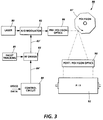
- Figure 3 is a schematic representation of a pulsed imaging, pulse width modulation, facet tracked ROS system.
- a focused beam of light from a laser 80 is applied to acoustooptic (A/O) modulator 82.
- a control circuit 84 converts an image bitmap video data stream into an analog video data stream consisting of a plurality of pixel periods, each period having a signal content representing charged area (black), discharge image area (color) and intermediate discharge (white) to be formed on the surface of photoreceptor 92.
- Circuit 84 controls the drive level of modulator 82.
- the light output profile emerging from modulator 82 is defined by the overlap of the acoustic pulses and the illuminating light beam from laser 80 and enables individual acoustic pulses to be imaged onto photoreceptor 92.
- the anamorphic prepolygon optics 86 performs a Fourier transformation of the optical pulses exiting the A/O modulator, and projects the Fourier profile onto facets 87 of rotating polygon 88.
- the polygon is placed at the back focal plane of the post polygon optics 90 and the front focal plane of the prepolygon optics 86.
- the frequency of the rf used to excite the modulator is swept in synchronism with the scanning across the photoreceptor by means of facet tracking circuit 81 and rf driver circuit 83 so that the Fourier profile remains centered on the facets 87 of the rotating polygon 88.
- the size of the zero order spot at the facet is dependent on, and is inversely proportional to, the size of the beam in the modulator, with the diffracted orders also exhibiting this same beam size.
- the beam in the modulator is small, as it would be in a prior art flying spot scanning system, or "shallow" pulse imaged system, then the zero order beam size as well as the beam size of the diffracted orders (96' and 98') will be large, and even the beams of the highest diffracted orders will overlap the zero order beam. If the beam in the modulator is large, as it would be in the "deep" pulse imaged system of the present invention, then the zero order beam 94 size at the facet will be small, as will the beam size of the diffracted orders 96 and 98.
- the average light level that passes through the modulator is proportional to the duty cycle of the pulse stream.
- the sideband energy does not pass beyond the facet, the average light level is further reduced, the actual reduction depending on the higher harmonic content that is passed to the acoustic wave.
- pulse width modulation at a 50% duty cycle will result in an exposure level of about 25%.
- the optical image of the acoustooptic video pattern is swept across the surface of photoreceptor 92, after passing through post polygon optics 90.
- Acoustic image motion at the photoreceptor surface which, if uncorrected, would blur the optical image, is cancelled by balancing the acoustic and scan velocities with the prepolygon and postpolygon optics magnification, resulting in the acoustic image remaining stationary on the photoreceptor.
- the imaged line is exposed at three exposure levels, zero, intermediate and full as shown in Figure 2a.
- the intermediate (white) exposure level is obtained from the pulse width narrowed video signals which become spatially narrow optical pulses exiting the modulator 82 and are filtered by facets 87 to result in a low uniform exposure at the photoreceptor 92.
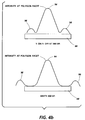
- Figure 4b shows a representation of the beam intensity at polygon facet 84 and demonstrates that an acoustooptic video stream alternating between one pixel on, and one pixel off, will produce an irradiance profile in the Fourier plane consisting of a single centered diffraction lobe (zero order beam) 94 and additional lobes 96,98 that correspond to the pattern frequency.
- each facet acts as a Fourier plane spatial frequency bandpass filter that limits the upper frequency that is reflected to the photoreceptor.
- the frequency associated with a 1-on/1-off pattern is passed through the optical system, thereby allowing printing of that frequency.
- the lower half of Figure 4 shows the diffraction pattern for printing a uniform intermediate exposure.
- the pulse width modulated video pattern is turned on and off for each pixel, with the on time corresponding to the desired exposure level.
- the frequency of this pattern is twice that of the 1-on/1-off pattern and thus, the associated diffraction lobes fall off the polygon facet, whose facet width has been appropriately designed.
- This spatial frequency filtering of the optical signal results in a uniform intermediate level output.
- the spatial filtering may also be accomplished by providing a discrete spatial filter of appropriate design in the optical path between the pre-polygon optics 86 and the polygon 88.
- the filter could be adapted to move synchronously with the polygon.
- FIG. 3 The scanning system of Figure 3 may be subject to a color line growth problem.
- Figure 5 shows the calculated exposure distribution (dashed curve 100) for a single red pixel video pulse 102 on a white background (video for white pixels 104) and, for comparative purposes, the exposure distribution for a red pixel on a black background is shown as 106.
- Each white and red pixel video pulse is centered in the associated pixel time frame.
- the exposure distribution for a red line on the white background is seen as much wider than the red pixel on black background (the exposure distribution for the red line on black background has the desired width).
- the color line growth is seen as directly caused by the width of the red line exposure distribution produced in this video setting.
- the color line growth problem is created by a coherent optical effect that causes the exposure distribution for a colored pixel to be wider than desired. It will be assumed that the color pixel, for purposes of further description, is a red pixel.
- Figure 6 shows an idealized electric field amplitude exiting the modulator of the ROS system shown in Figure 3 for a pattern consisting of a single pixel process direction red line on a white background.
- Figures 7 through 9 represent a modeling scheme that examines the behavior of the red and white pixels under convolution (a technique described in detail in The Fourier Transform and its Applications by R.M.
- the filtering of the optical system is such that the pixel frequency is not passed at the Fourier plane (facet 87, Figure 3), and therefore the white pattern has essentially zero modulation at photoreceptor 92. That is, the convolution of a repetitive white pixel pattern in the modulator with the optical transfer function gives a uniform output at the photoreceptor.
- the measured line Full Width at Half Maximum values (FWHM) will not be predicted by the variance calculations because electric field amplitude distributions, not exposure distributions (integrated irradiance), are being considered.
- FWHM Full Width at Half Maximum values
- Another aspect of the approximation is that the exposure distribution of a red line is not truly a Gaussian; variance and standard deviation do not relate exactly to the FWHM of an arbitrarily shaped distribution.
- the model allows a prediction of the relationship between red lines on white and black backgrounds, as well as the dependence of red lines as the white level is varied.
- the linearity of the convolution operator permits splitting the input distribution into several parts, performing the convolution with each part, and then combining the results.
- the distribution will be split into an all white pattern and a pattern containing two narrow rectangles.
- This modeling scheme treats a red pixel to be a white pixel plus a narrow rectangle of the same amplitude added to each side to fill the raster spacing shown in Figure 7.
- the periodic pattern in Figure 7(a) is filtered to be essentially constant.
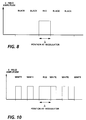
- the red on black case is shown in Figure 8.
- the behavior of variance under convolution allows an approximate prediction of the relative FWHM values of the cases shown in Figures 7b and 8. This is possible because the FWHM of a "Gaussian like" distribution is roughly proportional to the standard deviation of the distribution, which is equal to the square root of the variance.
- the distributions of interest here are the optical spread function and the "objects" that are imaged to form the line: the two rectangles in Figure 9(a) for a red line on a white background and the single rectangle of Figure 9(b) for the red-on-black case.
- the convolution/variance theorem states that variances add under convolution. Since the optical spread function is the same for all images, a comparison of the variances of the input lines determines the relationship of their output widths.
- the variance of the red-on-white "object” is greater than the variance of the red-on-black object (quantitative expressions are given in Figure 9). This can be understood intuitively by noting that the red-on-white "object” has energy only at the extreme ends of its addressable space, while the red-on-black object has energy at the ends but also in the middle of its addressable space. It is this dispersion of energy in the red-on-white object that causes its FWHM to be larger than that of the red-on-black case. For the case shown in Figure 9, the variance ratio is 1.76 (0.146/0.083) for red-on-white compared to red-on-black.
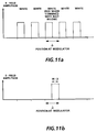
- Figure 10 shows an idealized electric field exiting the modulator when a correction scheme is employed to thin a single pixel red line.
- the pattern is separated into a periodic part that will be filtered to be essentially constant and the remaining part, which is the object that is imaged to form the line.
- Figure 11 shows the separated parts and we see that the object for line formation is compact as opposed to the dispersed object shown in Figure 7(b) (uncorrected case).
- the segmented image is filtered to be essentially constant
- Figure 11(b) shows the remaining pulses which form the red line.
- the imaged line must have a smaller variance (be thinner) in the corrected case.
- Figure 12a is a block diagram of a portion of control circuit 84 showing the video path for the creation of pulse width modulated tri-level images.
- Video 1 signal (130) and video 2 signal (131) are the two input lines needed to encode the three different video outputs, i.e., black, white and color.
- Arbitration circuits 133 and 134 are used for test pattern generation and beam control signals.
- a clock (CLK) signal 136 synchronized with polygon sweep, is used to clock the video through the system.
- the Pulse Width Modulation (PWM) circuit 138 takes the CLK 136 and a PWM control signal 140 which defines the desired pulse width for white pixels and outputs the PWM waveform 142 used to gate the rf drive signal 83' to the A/O modulator 82 ( Figure 3).
- the arbitration circuitry 134 generates a composite video signal 84' to the rf drive to generate black, color, and white pixels as called for by the video 130 and video 131 data signals.
- Figure 12b shows how a programmable delay in the pulse width modulation circuit 138 is used to translate the multiple bit PWM control signal into the needed PWM waveform.
- the CLK signal 136 is converted to a trigger 144 which is applied to a programmable delay pulse generator 145.
- the trigger is also applied to the set of a set/reset circuit 146 which generates the white PWM video signal 147.
- the PWM reset signal 148 which is a precisely delayed version of the trigger 144 which turned on the PWM video 142, is used to turn off the PWM video signal.
- the timing diagram 150 illustrates the relationships described above.
- Generator 145 for example, is a Brooktree Bt 604 dynamically programmed time edge vernier coupled to a digital-to-analog converter which controls the range of delays achievable.
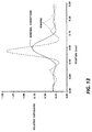
- Figure 13 shows the exposure distribution for an uncorrected single pixel red line (solid distribution line) and a corrected red line (dotted distribution line) using the technique described above to shift the white pulses to the start of the white pixel periods.
- the corrected line has been effectively thinned by nearly a pixel (40.1 ⁇ m: 127.9 ⁇ m for uncorrected; 87.8 ⁇ m for corrected measured at the 50% red bias level).
- a slight degree of ringing in the neighboring white region is present in the corrected case but does not adversely effect print quality.
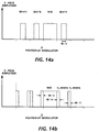
- PWPM circuit 138 is modified to divide each white pulse into two equal pulses, each pulse shifted to the outside edge of each pixel frame, as shown in Figure 14.
- the above described techniques each involve shifting the position of all white pixel pulses away from the conventional center position within the pixel period.
- a different class of color line growth solutions is directed towards identifying, in the video data input, white pixel and red pixel neighbor pairs, and performing various operations to effectively narrow one or the other of the pulses, or move only the white pulses that neighbor red pulses.
- the video data is buffered in white/red discriminator buffer circuit 120, where groups of pixels are successively buffered and bit match searching accomplished to determine the relationship of the pixels.
- the output of circuit 120 is sent along two paths to RAMS 121, 122.
- the RAMS store the video pulse characteristics in mapping tables and enable mapping any allowable video data word to any allowable video pulse characteristic.
- the outputs of RAMS 121,122 are sent to programmable delay circuits 123, 124, respectively. These delay circuits process the input signals from their respective RAMS to provide variable delays for the beginning and end of the video pulses.
- the pulse widths are determined by the difference between the two output delay signals.
- the outputs are applied to set/reset circuit 125 which generates the composite video signal.
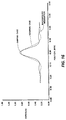
- Figure 17 shows the various pulse width and position combinations possible by circuit 138. To implement this first example, white pixels that are identified as being adjacent to a red pixel, are shifted by a distance appropriate to the total pixel addressability. For example, if the pixel addressability is 83 ⁇ m, a 5% shift of 4.2 ⁇ m would be appropriate. Figure 16 shows the effects of such a shift in the exposure distribution.
- a white pixel e.g. pixel 107 shown in Figure 5
- pixel 107 is shifted from its nominal (unshifted) position to a modified pulse shape that is narrower and with a higher peak.
- the same shifting would be performed on white pixel 108.
- An engineering trade off may have to be made to a slight increase in neighboring background modulation.
- an alternate technique is to narrow the white pixels; e.g. 107, 108, which have been identified as being adjacent a red pixel, e.g. 102, in buffering circuit 120.
- Figure 18 shows the case where the neighboring white pixels, 107 and 108 have been narrowed from a nominal 50% width to a 40% width.
- background modulation may increase.
- the white level may be varied for changes in copy mode of the imaging system, or to compensate for machine and environment fluctuations.
- the pixel operation is modified by utilizing a look up table 126 ( Figure 15) which generates a signal in response to a white exposure level change signal.
- the pixel shifting or narrowing is modified as a function of the white exposure level.
- a still further technique is to modify the red pixels only.
- the video data stream is again examined in buffer 120; each red pixel identified has its video pulse width narrowed.
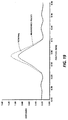
- Figure 19 shows the case where two red pixel pulse widths have been reduced by 10%.
- the tradeoff for this solution is some loss of contrast.
- An alternative operation on red pixels, identified in buffer 120 is to modify only the lead and trail edge of pixels leading and trailing in a red line. Once a group of red pixels constituting a red line are identified, the lead edge of the lead red pixel and the trail edge of the trailing red pixel are trimmed. The interior red pixels are left unchanged. A trim of about 6% off each line end produces satisfactory separation from neighboring white pixels. This technique results in improved contrast over the previous red pixel narrowing techniques since energy is not removed from the central part of the line.
- the system may be operable in a conventional white/black mode or an executive mode (white and red pixels only).
- the circuits enabling the above techniques can also be used to operate in the non tri-level modes, e.g. if the printer were operating in color executive mode (white and color pixels only), the white pulse conversion would be applied to all the white pixels in the video pulse stream. If the printer were operating in the black executive mode (white and black pixels only), the non modified video stream, e.g. the original video pulse structure would be used.
Landscapes
- Physics & Mathematics (AREA)
- Engineering & Computer Science (AREA)
- Optics & Photonics (AREA)
- General Engineering & Computer Science (AREA)
- General Physics & Mathematics (AREA)
- Theoretical Computer Science (AREA)
- Multimedia (AREA)
- Signal Processing (AREA)
- Facsimile Scanning Arrangements (AREA)
- Color Electrophotography (AREA)
- Mechanical Optical Scanning Systems (AREA)
- Fax Reproducing Arrangements (AREA)
- Color, Gradation (AREA)
Applications Claiming Priority (2)
| Application Number | Priority Date | Filing Date | Title |
|---|---|---|---|
| US07/756,643 US5260799A (en) | 1991-09-09 | 1991-09-09 | Pulsed imaging, pulse width modulation scanner for a tri-level highlight color imaging system |
| US756643 | 1991-09-09 |
Publications (3)
| Publication Number | Publication Date |
|---|---|
| EP0532180A2 true EP0532180A2 (fr) | 1993-03-17 |
| EP0532180A3 EP0532180A3 (en) | 1993-09-08 |
| EP0532180B1 EP0532180B1 (fr) | 1998-05-20 |
Family
ID=25044417
Family Applications (1)
| Application Number | Title | Priority Date | Filing Date |
|---|---|---|---|
| EP92307375A Expired - Lifetime EP0532180B1 (fr) | 1991-09-09 | 1992-08-12 | Analyseur d'image à modulation de la largeur d'impulsions pour un système de traitement d'images avec accentuation de couleurs à trois niveaux |
Country Status (7)
| Country | Link |
|---|---|
| US (1) | US5260799A (fr) |
| EP (1) | EP0532180B1 (fr) |
| JP (1) | JP2568355B2 (fr) |
| BR (1) | BR9203358A (fr) |
| CA (1) | CA2077293C (fr) |
| DE (1) | DE69225548T2 (fr) |
| MX (1) | MX9204581A (fr) |
Cited By (1)
| Publication number | Priority date | Publication date | Assignee | Title |
|---|---|---|---|---|
| US7031025B1 (en) | 2000-08-23 | 2006-04-18 | Hewlett-Packard Development Company, L.P. | Combined dot density and dot size modulation |
Families Citing this family (14)
| Publication number | Priority date | Publication date | Assignee | Title |
|---|---|---|---|---|
| US6169559B1 (en) * | 1992-11-18 | 2001-01-02 | Xerox Corporation | Hi-lite color ROS scan uniformity self correction architecture |
| JPH06262802A (ja) * | 1993-03-12 | 1994-09-20 | Konica Corp | 画像形成装置 |
| US5479175A (en) * | 1993-09-10 | 1995-12-26 | Xerox Corporation | Method and apparatus for enhancing discharged area developed regions in a tri-level pringing system |
| US5581292A (en) * | 1993-09-10 | 1996-12-03 | Xerox Corporation | Method and apparatus for enhancing charged area developed regions in a tri-level printing system |
| GB9318804D0 (en) * | 1993-09-10 | 1993-10-27 | Ici Plc | Optical data recordal |
| US5550653A (en) * | 1995-06-05 | 1996-08-27 | Xerox Corporation | Color sensor array and system for scanning simple color documents |
| JPH1078688A (ja) * | 1996-09-05 | 1998-03-24 | Hitachi Ltd | カラー画像形成装置 |
| JPH11205603A (ja) * | 1998-01-19 | 1999-07-30 | Toshiba Corp | 画像処理装置と画像形成装置 |
| US6285463B1 (en) * | 1998-12-22 | 2001-09-04 | Xerox Corporation | Method and apparatus for image compensation of blooming artifacts |
| US6426802B1 (en) | 1999-01-19 | 2002-07-30 | Xerox Corporation | Complementary halftone screens for highlight printing |
| US7253924B2 (en) * | 2003-01-31 | 2007-08-07 | Eastman Kodak Company | Method of imaging multiple binary bitmaps in a single pass |
| US7286155B1 (en) * | 2003-05-30 | 2007-10-23 | Silicon Light Machines Corporation | Optical engine using one-dimensional MEMS device |
| JP5839838B2 (ja) * | 2010-08-10 | 2016-01-06 | キヤノン株式会社 | 画像形成装置 |
| US10754012B2 (en) | 2019-01-04 | 2020-08-25 | Blackmore Sensors & Analytics, Llc | Lidar system including multifaceted deflector |
Family Cites Families (5)
| Publication number | Priority date | Publication date | Assignee | Title |
|---|---|---|---|---|
| JPS63136875A (ja) * | 1986-11-28 | 1988-06-09 | Ricoh Co Ltd | 画像形成装置 |
| JPS63290752A (ja) * | 1987-05-25 | 1988-11-28 | Ricoh Co Ltd | 画像形成装置 |
| US5066979A (en) * | 1989-01-13 | 1991-11-19 | Canon Kabushiki Kaisha | Color image forming apparatus wherein plural colors can be formed through one printing cycle |
| US4990955A (en) * | 1989-04-10 | 1991-02-05 | Xerox Corporation | White level stabilization for tri-level imaging |
| US5124802A (en) * | 1989-09-26 | 1992-06-23 | Canon Kabushiki Kaisha | Electrostatic lasar printer with a short side length of a modulation area formed by pulse width modulation set relative to a detected toner particle size |
-
1991
- 1991-09-09 US US07/756,643 patent/US5260799A/en not_active Expired - Fee Related
-
1992
- 1992-08-07 MX MX9204581A patent/MX9204581A/es unknown
- 1992-08-12 DE DE69225548T patent/DE69225548T2/de not_active Expired - Fee Related
- 1992-08-12 EP EP92307375A patent/EP0532180B1/fr not_active Expired - Lifetime
- 1992-08-26 JP JP4250715A patent/JP2568355B2/ja not_active Expired - Lifetime
- 1992-08-27 BR BR929203358A patent/BR9203358A/pt not_active IP Right Cessation
- 1992-09-01 CA CA002077293A patent/CA2077293C/fr not_active Expired - Fee Related
Cited By (1)
| Publication number | Priority date | Publication date | Assignee | Title |
|---|---|---|---|---|
| US7031025B1 (en) | 2000-08-23 | 2006-04-18 | Hewlett-Packard Development Company, L.P. | Combined dot density and dot size modulation |
Also Published As
| Publication number | Publication date |
|---|---|
| US5260799A (en) | 1993-11-09 |
| JPH05219312A (ja) | 1993-08-27 |
| JP2568355B2 (ja) | 1997-01-08 |
| EP0532180B1 (fr) | 1998-05-20 |
| EP0532180A3 (en) | 1993-09-08 |
| CA2077293A1 (fr) | 1993-03-10 |
| BR9203358A (pt) | 1993-04-13 |
| DE69225548D1 (de) | 1998-06-25 |
| DE69225548T2 (de) | 1998-12-03 |
| MX9204581A (es) | 1993-03-01 |
| CA2077293C (fr) | 1997-03-25 |
Similar Documents
| Publication | Publication Date | Title |
|---|---|---|
| US5260799A (en) | Pulsed imaging, pulse width modulation scanner for a tri-level highlight color imaging system | |
| US5223857A (en) | Pulsed imaging, pulse width modulation raster output scanner for tri-level exposure | |
| EP0162259B1 (fr) | Techniques à action réciproque pour relever la qualité d'impression | |
| EP0246457B1 (fr) | Compensation pour l'impression de lignes fines | |
| US5223906A (en) | Four color toner single pass color printing system using two tri-level xerographic units | |
| US5221954A (en) | Single pass full color printing system using a quad-level xerographic unit | |
| US5479175A (en) | Method and apparatus for enhancing discharged area developed regions in a tri-level pringing system | |
| US5500670A (en) | Asymmetric spatial filtering for pulsed imaging, pulse width modulation raster output scanner with tri-level exposure | |
| US5581292A (en) | Method and apparatus for enhancing charged area developed regions in a tri-level printing system | |
| US5081477A (en) | Method and apparatus for synchronizing the pel clock of a laser printer | |
| US6219085B1 (en) | Method and system for improved performance of adjustable printer clocks in an electrophotographic device | |
| US5561455A (en) | Color image forming apparatus | |
| EP1705896A2 (fr) | Procédé et système de contrôle de balayage par trame dans un système électrophotographique | |
| US5737008A (en) | Electrophotographic image recording apparatus with photoreceptor exposure control | |
| JPH04289880A (ja) | 露光装置 | |
| JPS63241576A (ja) | 画像記録装置 | |
| JPH01204747A (ja) | 画像記録装置 |
Legal Events
| Date | Code | Title | Description |
|---|---|---|---|
| PUAI | Public reference made under article 153(3) epc to a published international application that has entered the european phase |
Free format text: ORIGINAL CODE: 0009012 |
|
| AK | Designated contracting states |
Kind code of ref document: A2 Designated state(s): DE FR GB |
|
| PUAL | Search report despatched |
Free format text: ORIGINAL CODE: 0009013 |
|
| AK | Designated contracting states |
Kind code of ref document: A3 Designated state(s): DE FR GB |
|
| 17P | Request for examination filed |
Effective date: 19940228 |
|
| 17Q | First examination report despatched |
Effective date: 19960207 |
|
| GRAG | Despatch of communication of intention to grant |
Free format text: ORIGINAL CODE: EPIDOS AGRA |
|
| GRAG | Despatch of communication of intention to grant |
Free format text: ORIGINAL CODE: EPIDOS AGRA |
|
| GRAH | Despatch of communication of intention to grant a patent |
Free format text: ORIGINAL CODE: EPIDOS IGRA |
|
| GRAH | Despatch of communication of intention to grant a patent |
Free format text: ORIGINAL CODE: EPIDOS IGRA |
|
| GRAA | (expected) grant |
Free format text: ORIGINAL CODE: 0009210 |
|
| AK | Designated contracting states |
Kind code of ref document: B1 Designated state(s): DE FR GB |
|
| REF | Corresponds to: |
Ref document number: 69225548 Country of ref document: DE Date of ref document: 19980625 |
|
| ET | Fr: translation filed | ||
| PLBE | No opposition filed within time limit |
Free format text: ORIGINAL CODE: 0009261 |
|
| STAA | Information on the status of an ep patent application or granted ep patent |
Free format text: STATUS: NO OPPOSITION FILED WITHIN TIME LIMIT |
|
| 26N | No opposition filed | ||
| PGFP | Annual fee paid to national office [announced via postgrant information from national office to epo] |
Ref country code: DE Payment date: 20000807 Year of fee payment: 9 |
|
| PGFP | Annual fee paid to national office [announced via postgrant information from national office to epo] |
Ref country code: GB Payment date: 20000809 Year of fee payment: 9 |
|
| PGFP | Annual fee paid to national office [announced via postgrant information from national office to epo] |
Ref country code: FR Payment date: 20000811 Year of fee payment: 9 |
|
| PG25 | Lapsed in a contracting state [announced via postgrant information from national office to epo] |
Ref country code: GB Free format text: LAPSE BECAUSE OF NON-PAYMENT OF DUE FEES Effective date: 20010812 |
|
| GBPC | Gb: european patent ceased through non-payment of renewal fee |
Effective date: 20010812 |
|
| PG25 | Lapsed in a contracting state [announced via postgrant information from national office to epo] |
Ref country code: FR Free format text: LAPSE BECAUSE OF NON-PAYMENT OF DUE FEES Effective date: 20020430 |
|
| PG25 | Lapsed in a contracting state [announced via postgrant information from national office to epo] |
Ref country code: DE Free format text: LAPSE BECAUSE OF NON-PAYMENT OF DUE FEES Effective date: 20020501 |
|
| REG | Reference to a national code |
Ref country code: FR Ref legal event code: ST |