EP0533488A2 - Image sensing apparatus having two image sensing portions and one signal processing portion and allowing improved white balance control - Google Patents
Image sensing apparatus having two image sensing portions and one signal processing portion and allowing improved white balance control Download PDFInfo
- Publication number
- EP0533488A2 EP0533488A2 EP92308524A EP92308524A EP0533488A2 EP 0533488 A2 EP0533488 A2 EP 0533488A2 EP 92308524 A EP92308524 A EP 92308524A EP 92308524 A EP92308524 A EP 92308524A EP 0533488 A2 EP0533488 A2 EP 0533488A2
- Authority
- EP
- European Patent Office
- Prior art keywords
- signal
- image sensing
- white balance
- control
- signal processing
- Prior art date
- Legal status (The legal status is an assumption and is not a legal conclusion. Google has not performed a legal analysis and makes no representation as to the accuracy of the status listed.)
- Granted
Links
Images




Classifications
-
- H—ELECTRICITY
- H04—ELECTRIC COMMUNICATION TECHNIQUE
- H04N—PICTORIAL COMMUNICATION, e.g. TELEVISION
- H04N23/00—Cameras or camera modules comprising electronic image sensors; Control thereof
- H04N23/80—Camera processing pipelines; Components thereof
- H04N23/84—Camera processing pipelines; Components thereof for processing colour signals
- H04N23/88—Camera processing pipelines; Components thereof for processing colour signals for colour balance, e.g. white-balance circuits or colour temperature control
-
- H—ELECTRICITY
- H03—ELECTRONIC CIRCUITRY
- H03M—CODING; DECODING; CODE CONVERSION IN GENERAL
- H03M1/00—Analogue/digital conversion; Digital/analogue conversion
- H03M1/66—Digital/analogue converters
-
- H—ELECTRICITY
- H01—ELECTRIC ELEMENTS
- H01H—ELECTRIC SWITCHES; RELAYS; SELECTORS; EMERGENCY PROTECTIVE DEVICES
- H01H2231/00—Applications
- H01H2231/046—Camera
Definitions
- the present invention relates generally to image sensing apparatuses, and more specifically, to an auto white balance circuit for use in an image sensing apparatus such as a video camera.
- a further object of the invention is to conduct quick white balance control in an image sensing apparatus having two image sensing portions and one signal processing portion.
- an image sensing apparatus in accordance with the invention includes a first image sensing portion for sensing the image of an object and outputting a first signal, a second image sensing portion for sensing the image of an object and outputting a second signal, a signal processing device for subjecting the input signal to a prescribed processing for output, a first switch for selecting one of the output first signal and second signal and applying the selected one to the signal processing device, a control signal generation device for generating a first control signal for the signal processing device to conduct a prescribed processing to the first signal and a second control signal for the signal processing device to conduct a prescribed processing to the second signal, a second switch for selecting one of the generated first control signal and second control signal and applying the selected one to the signal processing device, and a controller for controlling the first switch so that the switch selects one of the first signal and the second signal, and controlling the second switch so that the switch selects the first control signal or the second control signal corresponding to the selected first signal or second signal.
- the signal selected from the image sensing portions A or B is divided into chrominance signal components RGB, from which color difference signals R-Y and B-Y are formed and input into an encoder 9.
- a luminance signal and a chrominance signal are produced and then mixed to form a video signal which is output to a succeeding stage circuit (not shown).
- the microcomputer 11 decides white balance control values Rcont ⁇ A and Bcont ⁇ A for the image sensing portion A, and transmits these control values to the D/A converter 12 using three lines, CLK, DATA, and LD.
- the D/A converter 12 conducts D/A conversion based on the incoming data and generates DC voltages.
- the DC voltages are supplied to the Rcont and Bcont terminals of the signal processing portion 8 through analog switches 13 and 14.
- the estimated Rcont ⁇ B and Bcont ⁇ B are, as is the case with the Rcont ⁇ A and Bcont ⁇ A, transmitted to the D/A converter 12 using three lines, CLK, DATA, and LD from the microcomputer 11, and converted into DC voltages at the D/A converter 12 for input to the analog switches 13 and 14. At that time, with the analog switches 13 and 14 being set to pass Rcont ⁇ A and Bcont ⁇ A, Rcont ⁇ B and Bcont ⁇ B are not applied to the signal processing portion 8.
- the microcomputer 11 When the microcomputer 11 receives as a switching signal an instruction of switching between the image sensing portions A and B from an external portion (operation key), the microcomputer 11 does not have to make a control to the D/A converter 12, but simply switches the analog switches 7, 13 and 14 by inverting switch control. This is because Rcont ⁇ B and Bcont ⁇ B from the D/A converter are immediately applied to signal processing circuit 8 through the switches 13 and 14. Thereafter, the RGB signals from the image sensing portion B are input into the microcomputer 11 from the signal processing circuit 8 through the integrated circuit 10 with a delay of the time constant of the integrated circuit 10, and the white balance control values Rcont ⁇ B and Bcont ⁇ B for the image sensing portion B are determined based on the signals. Then, based on the determined control values Rcont ⁇ B and Bcont ⁇ B the microcomputer 11 estimates white balance control values Rcont ⁇ A and Bcont ⁇ A for the image sensing portion A.
- a high speed control operation of the microcomputer 11 to the switches 7, 13, and 14 permits composing outputs from the image sensing portions A and B. For example, suppose that a part of a picture frame from the image sensing portion A is placed in a picture frame from the image sensing portion B. In this case, if the area of the image sensing portion A is wide enough as compared to the area of the image sensing portion B, RGB signals input to the microcomputer can be considered as signals from the image sensing portion A.
- the Rcont ⁇ A and Bcont ⁇ A are determined, the Rcont ⁇ B and Bcont ⁇ B are estimated, and the respective control values are transmitted to the D/A converter 12.
- the output of D/A converter 12 is selected by the analog switches 13 and 14 for input to the signal processing portion 8.
- a high speed switch control by the microcomputer 11 permits the control voltages Rcont ⁇ A and Bcont ⁇ A to be applied to the portion corresponding to the picture frame of the image sensing portion A, and control voltages Rcont ⁇ B nd Bcont ⁇ B to be applied to the portion corresponding to the picture frame of the image sensing portion B, thereby achieving stable white balance.
- a second embodiment of the invention follows in conjunction with Fig. 2.
- the same reference characters as Fig. 1 denote the same or corresponding portions in Fig. 2.
- white balance operation is achieved by an interruption of a vertical pulse VD in synchronization with a vertical synchronizing signal.
- White balance is set to work only in response to a completion of a certain number of interruptions of the vertical pulse VD, not for every interruption of the vertical pulse VD.
- a VD counter is provided in a microcomputer 11b in a programming manner.
- white balance operation is conducted even with a smaller number of interruptions of the vertical pulse VD as compared to an usual state. This means time until initiation of the white balance operation is reduced when switching between the image sensing portions.
- step #20 a determination whether or not a switching signal is externally input from other microcomputers, switches, or the like to the microcomputer 11b is made in step #20. Then, if the switching signal is input, the microcomputer 11b proceeds to step #35, controls the analog switches 7, 13, 14 by its switch control, and switches between the outputs of the image sensing portions A, B and D/A converter 12. Then, in step #45, the value of the VD counter is set to a value for high speed operation, for example, 4VD, thus completing the interruption routine. Thus, the auto white balance operation is conducted at a high speed.
- step #20 If in the above-stated step #20 there is not any switching signal, a determination whether or not white balance operation is presently going on at a high speed is made in the next step #25 and if the high speed operation is going on, a determination whether or not a fixed time period has elapsed is conducted (step #40), and if the fixed time has not yet elapsed, the high speed operation is continued (step #45). If the white balance operation is not going on at a high speed, or it is going on at a high speed but the fixed time period has already run out, the value of the VD counter is set to a value for usual operation 12VD, for example, in step #30, thus completing the interruption routine. Thus, after the elapsed time of 12VD counting value, the auto white balance operation will be resumed.
- FIG. 4 A description of a third embodiment of the invention follows in conjunction with a block diagram shown in Fig. 4.
- Fig. 4 one of an output signal from an image sensing portion A formed of an image sensing lens 1, a CCD 2, and a CDS ⁇ AGC circuit 3, and an output signal from an image sensing portion B formed of an image sensing lens 4, a CCD 5, and a CDS ⁇ AGC circuit 6 is selected by an analog switch 7 and input to a signal processing portion 8.
- the signal from the image sensing portion is divided into chrominance signal components RGB, from which color difference signals R-Y and B-Y are formed to be input to an encoder 9.
- a luminance signal and a chrominance signal are produced and mixed to form a video signal to be output to a circuit of a succeeding stage (not shown).
- the RGB signals formed in the signal processing portion 8 are converted into DC voltages at an integrated circuit 10, and input into a microcomputer 11c.
- a control function is decided from control values Rcont and Bcont indoors which are stored in the microcomputer or an external EEPROM 20 at the time of manufacture and control values Rcont and Bcont outdoors (in some cases, in addition to these values, control values Rcont and Bcont under two or three kinds of fluorescent light), and based on the function, the Rcont and Bcont are controlled (see fa in Fig. 5 and fb in Fig. 6).
- the microcomputer 11c sets the analog switch 7 to select the output of the image sensing portion A by the function of the switch control output signal. At that time, only the signal of the image sensing portion A is input to the signal processing portion 8, and the white balance of the image sensing portion A is made by an auto white balance operation. Now, suppose that the control value of the image sensing portion A in an auto white balance operation resides at point X in Fig. 5. At that time, the following calculation is conducted for estimating the control value of the image sensing portion B to some extent.
- the microcomputer 11c switches its switch control for the analog switch 7, and switches the control values from the Rcont and Bcont to the control values at point Y which has been estimated from the control values of point X.
- point X is estimated from point Y and the control values are switched accordingly.
- the moment the image sensing portions are switched from one to the other white balance is substantially established, and stable white balance is provided when two picture frames are mixed into one.
Landscapes
- Engineering & Computer Science (AREA)
- Multimedia (AREA)
- Signal Processing (AREA)
- Theoretical Computer Science (AREA)
- Color Television Image Signal Generators (AREA)
- Processing Of Color Television Signals (AREA)
Abstract
Description
- The present invention relates generally to image sensing apparatuses, and more specifically, to an auto white balance circuit for use in an image sensing apparatus such as a video camera.
- When one desires to obtain two image frames at a time using a conventional video camera, one possible method is to select the outputs of two
independent video cameras VTR 18. - According to such a method, however, though white balance is stable with the video cameras being independent, a large system will be necessary to accommodate the two video cameras, which is disadvantageous in terms of cost or portability. Constructing a video camera to have two image sensing portions, one signal processing portion, and a switch portion for switching between the image sensing portions as disclosed in Japanese Patent Laying-Open No. 2-143683 provides a less costly image sensing apparatus. However in this case, when the image sensing portions are switched from one to the other, or when an image obtained from one image sensing portion is entered into a part of an image obtained from the image sensing portion by switching the switch at a high speed a number of times, white balance is gradually disordered, resulting in difficulty in viewing of a reproduced image.
- It is an object of the invention to improve the quality of a reproduced image in an image sensing apparatus having two image sensing portions and one signal processing portion.
- Another object of the invention is to achieve appropriate white balance in an image sensing apparatus having two image sensing portions and one signal processing portion.
- A further object of the invention is to conduct quick white balance control in an image sensing apparatus having two image sensing portions and one signal processing portion.
- In order to achieve the above-stated objects, an image sensing apparatus in accordance with the invention includes a first image sensing portion for sensing the image of an object and outputting a first signal, a second image sensing portion for sensing the image of an object and outputting a second signal, a signal processing device for subjecting the input signal to a prescribed processing for output, a first switch for selecting one of the output first signal and second signal and applying the selected one to the signal processing device, a control signal generation device for generating a first control signal for the signal processing device to conduct a prescribed processing to the first signal and a second control signal for the signal processing device to conduct a prescribed processing to the second signal, a second switch for selecting one of the generated first control signal and second control signal and applying the selected one to the signal processing device, and a controller for controlling the first switch so that the switch selects one of the first signal and the second signal, and controlling the second switch so that the switch selects the first control signal or the second control signal corresponding to the selected first signal or second signal.
- Thus constructed image sensing apparatus conducts a prescribed processing to a signal output from the switched image sensing portion based on a corresponding control signal, and the quality of a reproduced image is therefore improved.
- The foregoing and other objects, features, aspects and advantages of the present invention will become more apparent from the following detailed description of the present invention when taken in conjunction with the accompanying drawings.
-
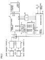
- Fig. 1 is a system block diagram showing a construction of an image sensing apparatus in accordance with a first embodiment of the invention;
- Fig. 2 is a system block diagram showing a construction of an image sensing apparatus in accordance with a second embodiment of the invention;
- Fig. 3 is a flow chart for use in illustration of the content of control executed by the microcomputer shown in Fig. 2;
- Fig. 4 is a system block diagram showing a construction of an image sensing apparatus in accordance with a third embodiment of the invention;
- Fig. 5 is a representation showing a control function for an image sensing portion A for use in white balance control executed by the microcomputer shown in Fig. 4;
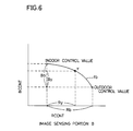
- Fig. 6 is a representation showing a control function for an image sensing portion B for use in white balance control executed by the microcomputer shown in Fig. 4; and
- Fig. 7 is a diagram showing arrangement of two conventional video cameras disposed in parallel.
-
- A first embodiment of the invention is illustrated as a block circuit in Fig. 1. In Fig. 1, one of an output signal from an image sensing portion A formed of an
image sensing lens 1, a CCD (Charge Coupled Device) 2, and a CDS (Correlating Double Sampling)· AGC (Auto Gain Control)circuit 3, and an output signal from an image sensing portion B formed of animage sensing lens 4, aCCD 5, and a CDS·AGC circuit 6 is selected by ananalog switch 7 and input into asignal processing portion 8. - In the
signal processing portion 8, the signal selected from the image sensing portions A or B is divided into chrominance signal components RGB, from which color difference signals R-Y and B-Y are formed and input into anencoder 9. In theencoder 9, a luminance signal and a chrominance signal are produced and then mixed to form a video signal which is output to a succeeding stage circuit (not shown). - In an auto white balance circuit of signal processing type, the RGB signals formed in the
signal processing portion 8 are converted into DC voltages in an integratedcircuit 10, and input to a microcomputer 11. The microcomputer 11 subjects each of the converted RGB signals to an A/D conversion, and supplies to a D/A converter 12 white balance control data of a signal level satisfying
switch 7 by its switch control, only a signal from the image sensing portion A is input to thesignal processing portion 8. Therefore, only RGB signals from the image sensing portion A are input to the microcomputer 11 through the integratedcircuit 10. Based on the RGB signals, the microcomputer 11 decides white balance control values Rcont·A and Bcont·A for the image sensing portion A, and transmits these control values to the D/A converter 12 using three lines, CLK, DATA, and LD. The D/A converter 12 conducts D/A conversion based on the incoming data and generates DC voltages. The DC voltages are supplied to the Rcont and Bcont terminals of thesignal processing portion 8 throughanalog switches - Meanwhile, a signal from the image sensing portion B is stopped by the function of the
analog switch 7 and not input to thesignal processing portion 8, but white balance control values Rcont·B and Bcont·B for the image sensing portion B are preferably estimated by a proportion calculation based on white balance control values Rcont·A and Bcont·A to the image sensing portion A. - The estimated Rcont·B and Bcont·B are, as is the case with the Rcont·A and Bcont·A, transmitted to the D/
A converter 12 using three lines, CLK, DATA, and LD from the microcomputer 11, and converted into DC voltages at the D/A converter 12 for input to theanalog switches analog switches signal processing portion 8. - When the microcomputer 11 receives as a switching signal an instruction of switching between the image sensing portions A and B from an external portion (operation key), the microcomputer 11 does not have to make a control to the D/
A converter 12, but simply switches theanalog switches signal processing circuit 8 through theswitches signal processing circuit 8 through the integratedcircuit 10 with a delay of the time constant of the integratedcircuit 10, and the white balance control values Rcont·B and Bcont·B for the image sensing portion B are determined based on the signals. Then, based on the determined control values Rcont·B and Bcont·B the microcomputer 11 estimates white balance control values Rcont·A and Bcont·A for the image sensing portion A. - A high speed control operation of the microcomputer 11 to the
switches - As described, the Rcont·A and Bcont·A are determined, the Rcont·B and Bcont·B are estimated, and the respective control values are transmitted to the D/
A converter 12. The output of D/A converter 12 is selected by the analog switches 13 and 14 for input to thesignal processing portion 8. A high speed switch control by the microcomputer 11 permits the control voltages Rcont·A and Bcont·A to be applied to the portion corresponding to the picture frame of the image sensing portion A, and control voltages Rcont·B nd Bcont·B to be applied to the portion corresponding to the picture frame of the image sensing portion B, thereby achieving stable white balance. - A description of a second embodiment of the invention follows in conjunction with Fig. 2. The same reference characters as Fig. 1 denote the same or corresponding portions in Fig. 2. In this embodiment, white balance operation is achieved by an interruption of a vertical pulse VD in synchronization with a vertical synchronizing signal. White balance is set to work only in response to a completion of a certain number of interruptions of the vertical pulse VD, not for every interruption of the vertical pulse VD. For this purpose, a VD counter is provided in a
microcomputer 11b in a programming manner. However, for a fixed period immediately after switching of the image sensing portions, white balance operation is conducted even with a smaller number of interruptions of the vertical pulse VD as compared to an usual state. This means time until initiation of the white balance operation is reduced when switching between the image sensing portions. - As illustrated by a flow chart in Fig. 3, when an interruption of the vertical pulse VD is made, the VD counter is decremented by 1 in
step # 5, and a determination whether or not the count value is 0 is made instep # 10. If the count value is not 0, the interruption routine is completed (step #50), and if the count value is 0, the operation proceeds to step #15, and white balance operation as described above is conducted. - After the auto white balance operation is completed, a determination whether or not a switching signal is externally input from other microcomputers, switches, or the like to the
microcomputer 11b is made instep # 20. Then, if the switching signal is input, themicrocomputer 11b proceeds to step #35, controls the analog switches 7, 13, 14 by its switch control, and switches between the outputs of the image sensing portions A, B and D/A converter 12. Then, instep # 45, the value of the VD counter is set to a value for high speed operation, for example, 4VD, thus completing the interruption routine. Thus, the auto white balance operation is conducted at a high speed. - If in the above-stated
step # 20 there is not any switching signal, a determination whether or not white balance operation is presently going on at a high speed is made in thenext step # 25 and if the high speed operation is going on, a determination whether or not a fixed time period has elapsed is conducted (step #40), and if the fixed time has not yet elapsed, the high speed operation is continued (step #45). If the white balance operation is not going on at a high speed, or it is going on at a high speed but the fixed time period has already run out, the value of the VD counter is set to a value for usual operation 12VD, for example, instep # 30, thus completing the interruption routine. Thus, after the elapsed time of 12VD counting value, the auto white balance operation will be resumed. - In the above-described operation, after a switching signal from an external portion (for example a key) is input and the image sensing portions are switched from one to the other, time until initiation of the auto white balance operation is reduced by the fixed time period.
- A description of a third embodiment of the invention follows in conjunction with a block diagram shown in Fig. 4. In Fig. 4, one of an output signal from an image sensing portion A formed of an
image sensing lens 1, aCCD 2, and a CDS·AGC circuit 3, and an output signal from an image sensing portion B formed of animage sensing lens 4, aCCD 5, and a CDS·AGC circuit 6 is selected by ananalog switch 7 and input to asignal processing portion 8. - At the
signal processing portion 8, the signal from the image sensing portion is divided into chrominance signal components RGB, from which color difference signals R-Y and B-Y are formed to be input to anencoder 9. At theencoder 9, a luminance signal and a chrominance signal are produced and mixed to form a video signal to be output to a circuit of a succeeding stage (not shown). - In an auto white balance circuit of a signal processing type, the RGB signals formed in the
signal processing portion 8 are converted into DC voltages at anintegrated circuit 10, and input into amicrocomputer 11c. Themicrocomputer 11c subjects them to an A/D conversion, and increases control signals Rcont, Bcont (Rcont and Bcont are DC voltages) to satisfy
- Generally, a control function is decided from control values Rcont and Bcont indoors which are stored in the microcomputer or an
external EEPROM 20 at the time of manufacture and control values Rcont and Bcont outdoors (in some cases, in addition to these values, control values Rcont and Bcont under two or three kinds of fluorescent light), and based on the function, the Rcont and Bcont are controlled (see fa in Fig. 5 and fb in Fig. 6). - Now, assume that the
microcomputer 11c sets theanalog switch 7 to select the output of the image sensing portion A by the function of the switch control output signal. At that time, only the signal of the image sensing portion A is input to thesignal processing portion 8, and the white balance of the image sensing portion A is made by an auto white balance operation. Now, suppose that the control value of the image sensing portion A in an auto white balance operation resides at point X in Fig. 5. At that time, the following calculation is conducted for estimating the control value of the image sensing portion B to some extent. - In Fig. 5, assume that the difference between the control value Rcont outdoors and the control value Rcont indoors is Ra, the difference between the control value Rcont at point X representing the control value at present and the control value Rcont indoors is Rx, while in Fig. 6, the difference between the control value Rcont outdoors of the image sensing portion B and the control value Rcont indoors is Rb, and the difference between the control value Rcont at point Y to be estimated and the control value Rcont indoors is Ry. Assuming that a proportional relation is established between these values, let


- When a switching is made from the image sensing portion A to the image sensing portion B, the
microcomputer 11c switches its switch control for theanalog switch 7, and switches the control values from the Rcont and Bcont to the control values at point Y which has been estimated from the control values of point X. Similarly, when a switching is made from the image sensing portion B to the image sensing portion A, point X is estimated from point Y and the control values are switched accordingly. - When the image sensing portions are switched by the above-stated operation, the control values which have been previously estimated are output, and a substantially white balance match state is achieved.
- As in the foregoing, according to the invention, the moment the image sensing portions are switched from one to the other, white balance is substantially established, and stable white balance is provided when two picture frames are mixed into one.
- According to the invention, when objects under different conditions are image-sensed by the two image sensing portions, white balance shift created by a switching operation can quickly be corrected, and white balance follows a switching between picture frames with an improved accuracy.
- Although the present invention has been described and illustrated in detail, it is clearly understood that the same is by way of illustration and example only and is not to be taken by way of limitation, the spirit and scope of the present invention being limited only by the terms of the appended claims.
Claims (12)
- An image sensing apparatus, comprising:
a first image sensing portion (A) for sensing the image of an object to output a first signal;
a second image sensing portion (B) for sensing the image of an object to output a second signal;
signal processing means (8) for subjecting an input signal to a prescribed processing to output a signal;
first switching means (7) for selecting one of said output first signal and second signal and applying the selected signal to said signal processing means;
control signal generation means (11a, 11b) for generating a first control signal for said signal processing means to conduct said prescribed processing to said first signal, and a second control signal for said signal processing means to conduct said prescribed processing to said second signal;
second switching means (13, 14) for selecting one of said generated first control signal and second control signal and applying the selected signal to said signal processing means; and
control means (11a, 11b) responsive to a switching signal for controlling said first switching means to select one of said first signal and second signal, and controlling said second switching means to select one of said first control signal and second control signal corresponding to said selected one of the first signal and second signal. - An image sensing apparatus recited in claim 1, wherein
said prescribed processing includes white balance control to the chrominance signal of the input signal. - An image sensing apparatus as recited in claim 2, wherein
said control signal generation means generates a white balance control value based on the chrominance signal of one of said first and second signals input to said signal processing means and to be subjected to said prescribed processing. - An image sensing apparatus as recited in claim 3, wherein
said control signal generation means conducts a prescribed operation based on said generated white balance control value to generate the white balance control value of the other signal of said first and second signals. - An image sensing apparatus, comprising:
two image sensing portions (A, B) each for sensing the image of an object to output a signal;
one system of signal processing portion (8) for subjecting an applied signal to a prescribed processing;
a first analog switch (7) for applying one of the outputs of said image sensing portions to said signal processing portion;
a digital/analog converter (12) for converting the digital amounts of first and second white balance control signals for said image sensing portions, respectively to analog amounts for output;
a second analog switch (13, 14) for selecting one of said first and second white balance control signals output from said digital/analog converter and applying the selected signal to said signal processing portion; and
control portions (11a, 11b) for controlling said digital/analog converter, and first and second analog switches. - An image sensing apparatus as recited in claim 5, wherein
said control portion is formed of a microcomputer, and said microcomputer forms said white balance control signal based on a chrominance signal from said signal processing portion and applies the signal to said digital/analog converter. - An image sensing apparatus having an auto white balance function formed of a signal processing portion (8) for processing signals applied from image sensing portions (A, B), and a control portion (11a, 11b) for applying a white balance control signal based on a chrominance signal applied from said signal processing portion to said control signal processing portion, comprising:
two image sensing portions each for sensing the image of an object to output a signal;
a first switch (7) for applying one of the outputs of said image sensing portions to said signal processing portion;
a second switch (13, 14) for selecting one of said white balance control signals respectively for said image sensing portions output from said control portion and applying the selected signal to said signal processing portion; and
control means (11a, 11b) for controlling switching between said first and second switches. - A white balance circuit for a video camera having two image sensing portions (A, B) and one signal processing portion (8) and capable of image-sensing by switching between said image sensing portions, comprising:
auto white balance control means (11a, 11b) for forming a white balance control signal based on a chrominance signal from said signal processing portion and conducting white balance control of the chrominance signal in said signal processing portion by said white balance control signal at prescribed intervals;
execution means for executing said white balance control at intervals shorter than said prescribed intervals in a time period for processing when said image sensing portions are switched between each other. - A white balance circuit as recited in claim 8, wherein
said prescribed interval is decided by a prescribed number of interruptions of a vertical pulse (VD) in synchronization with a vertical synchronizing signals. - A white balance circuit as recited in claim 9, wherein
when said image sensing portions are switched between each other, white balance control is executed by a smaller number of interruptions of the vertical pulse (VD) than said prescribed number. - An image sensing apparatus having an auto white balance function formed of a signal processing portion (8) for processing signals applied from image sensing portions (A, B) and a control portion (11c) for applying a white balance control signal formed based on a chrominance signal applied from said signal processing portion to said signal processing portion, comprising:
two image sensing portions each for sensing the image of an object to output a signal;
a switch portion (7) for applying one of the outputs of said image sensing portions to said signal processing portion;
storage means (20) for previously storing the white balance adjustment data of said image sensing portions;
estimation means (11c) for estimating a white balance control signal for an image sensing portion which is not selected at the moment based on said stored adjustment data and the white balance control signal for the image sensing portion selected at present; and
control means (11c) for setting said estimated white balance control signal as a white balance control signal for said switched image sensing portion, when the outputs of said image sensing portions are switched by said switch portion. - An image sensing apparatus as recited in claim 11, wherein
said adjustment data includes a white balance control value indoors and a white balance control value outdoors.
Applications Claiming Priority (4)
| Application Number | Priority Date | Filing Date | Title |
|---|---|---|---|
| JP3268758A JP2782697B2 (en) | 1991-09-19 | 1991-09-19 | Auto white balance circuit |
| JP268758/91 | 1991-09-19 | ||
| JP268757/91 | 1991-09-19 | ||
| JP3268757A JPH0583620A (en) | 1991-09-19 | 1991-09-19 | White balance circuit |
Publications (3)
| Publication Number | Publication Date |
|---|---|
| EP0533488A2 true EP0533488A2 (en) | 1993-03-24 |
| EP0533488A3 EP0533488A3 (en) | 1993-07-07 |
| EP0533488B1 EP0533488B1 (en) | 1997-04-23 |
Family
ID=26548464
Family Applications (1)
| Application Number | Title | Priority Date | Filing Date |
|---|---|---|---|
| EP92308524A Expired - Lifetime EP0533488B1 (en) | 1991-09-19 | 1992-09-18 | Image sensing apparatus having two image sensing portions and one signal processing portion and allowing improved white balance control |
Country Status (7)
| Country | Link |
|---|---|
| US (1) | US5267025A (en) |
| EP (1) | EP0533488B1 (en) |
| KR (1) | KR950008129B1 (en) |
| CA (1) | CA2078161C (en) |
| DE (1) | DE69219258T2 (en) |
| ES (1) | ES2101043T3 (en) |
| MY (1) | MY108780A (en) |
Cited By (3)
| Publication number | Priority date | Publication date | Assignee | Title |
|---|---|---|---|---|
| DE19514629A1 (en) * | 1995-04-26 | 1996-10-31 | Thomson Brandt Gmbh | Video camera with white balance correction |
| US7262796B2 (en) | 2000-11-01 | 2007-08-28 | Koninklijke Philips Electronics N.V. | Processing of color signals in a color camera |
| US7639283B1 (en) | 1998-08-14 | 2009-12-29 | Ipg Electronics 503 Limited | Color signal matrix adjustment |
Families Citing this family (6)
| Publication number | Priority date | Publication date | Assignee | Title |
|---|---|---|---|---|
| JP3003302B2 (en) * | 1991-07-17 | 2000-01-24 | ソニー株式会社 | Signal processing circuit and signal processing method for solid-state imaging device |
| US5589879A (en) * | 1993-03-26 | 1996-12-31 | Fuji Photo Film Co., Ltd. | Performing white balance correction on integrated divided areas of which average color is substantially white |
| US6407773B1 (en) | 1994-02-28 | 2002-06-18 | Canon Kabushiki Kaisha | Image sensing apparatus |
| DE69528918T2 (en) * | 1994-02-28 | 2003-04-24 | Canon K.K., Tokio/Tokyo | Imaging device |
| JP2001086414A (en) * | 1999-09-10 | 2001-03-30 | Sony Corp | Imaging device and signal processing method |
| KR100765251B1 (en) * | 2005-12-29 | 2007-10-09 | 엠텍비젼 주식회사 | White Balance Determination Method and Digital Imaging Apparatus Using the Same |
Family Cites Families (8)
| Publication number | Priority date | Publication date | Assignee | Title |
|---|---|---|---|---|
| JPS5857885A (en) * | 1981-10-01 | 1983-04-06 | Nippon Kogaku Kk <Nikon> | White balance device |
| JPS59196679A (en) * | 1983-04-22 | 1984-11-08 | Toshiba Corp | White balance adjusting system in plural color television cameras |
| FR2577669B1 (en) * | 1985-02-21 | 1992-05-15 | Fuji Photo Film Co Ltd | IMAGE READING METHOD AND APPARATUS |
| US4814864A (en) * | 1987-05-29 | 1989-03-21 | Eastman Kodak Co. | Video camera with automatic prescaling for color balance |
| US4901152A (en) * | 1987-08-31 | 1990-02-13 | Canon Kabushiki Kaisha | Image pickup apparatus |
| JP2565388B2 (en) * | 1988-11-24 | 1996-12-18 | 赤井電機株式会社 | Video camera equipment |
| DE3905591C2 (en) * | 1989-02-23 | 1997-08-28 | Rheinmetall Ind Ag | Device for obtaining high-contrast images |
| US5157499A (en) * | 1990-06-29 | 1992-10-20 | Kabushiki Kaisha N A C | High-speed video camera using solid-state image sensor |
-
1992
- 1992-09-14 MY MYPI92001641A patent/MY108780A/en unknown
- 1992-09-14 CA CA002078161A patent/CA2078161C/en not_active Expired - Fee Related
- 1992-09-18 KR KR1019920017019A patent/KR950008129B1/en not_active Expired - Fee Related
- 1992-09-18 ES ES92308524T patent/ES2101043T3/en not_active Expired - Lifetime
- 1992-09-18 DE DE69219258T patent/DE69219258T2/en not_active Expired - Lifetime
- 1992-09-18 US US07/946,605 patent/US5267025A/en not_active Expired - Lifetime
- 1992-09-18 EP EP92308524A patent/EP0533488B1/en not_active Expired - Lifetime
Cited By (3)
| Publication number | Priority date | Publication date | Assignee | Title |
|---|---|---|---|---|
| DE19514629A1 (en) * | 1995-04-26 | 1996-10-31 | Thomson Brandt Gmbh | Video camera with white balance correction |
| US7639283B1 (en) | 1998-08-14 | 2009-12-29 | Ipg Electronics 503 Limited | Color signal matrix adjustment |
| US7262796B2 (en) | 2000-11-01 | 2007-08-28 | Koninklijke Philips Electronics N.V. | Processing of color signals in a color camera |
Also Published As
| Publication number | Publication date |
|---|---|
| CA2078161C (en) | 1996-01-30 |
| DE69219258T2 (en) | 1997-10-30 |
| US5267025A (en) | 1993-11-30 |
| ES2101043T3 (en) | 1997-07-01 |
| EP0533488B1 (en) | 1997-04-23 |
| DE69219258D1 (en) | 1997-05-28 |
| KR950008129B1 (en) | 1995-07-25 |
| EP0533488A3 (en) | 1993-07-07 |
| CA2078161A1 (en) | 1993-03-20 |
| KR930007286A (en) | 1993-04-22 |
| MY108780A (en) | 1996-11-30 |
Similar Documents
| Publication | Publication Date | Title |
|---|---|---|
| US7136581B2 (en) | Image taking apparatus and program product | |
| US4274107A (en) | Memory-type automatic adjustment system | |
| US4959727A (en) | Image pick-up apparatus | |
| EP0503962A2 (en) | Image sensing apparatus having plurality of optical systems and method of operating such apparatus | |
| US7330206B2 (en) | Auto white balance controlling method and electronic camera | |
| US4901152A (en) | Image pickup apparatus | |
| US5267025A (en) | Image sensing apparatus having two image sensing portions and one signal processing portion and allowing improved white balance control | |
| EP0516460B1 (en) | Digital signal processing system for color camera apparatus | |
| KR100209456B1 (en) | Color imaging device | |
| US20060114334A1 (en) | Image pickup apparatus with function of rate conversion processing and control method therefor | |
| US5508739A (en) | White-balance adjusting apparatus and a method thereof for a video camera | |
| EP0368314A2 (en) | Television receiver | |
| KR0128089Y1 (en) | View-finder with color vector display | |
| US20010045984A1 (en) | Hue adjusting method and hue adjusting device | |
| JPH0230230B2 (en) | ||
| US5557325A (en) | Video camera and its control method | |
| JPS62132490A (en) | White balance correction circuit | |
| JP3754425B2 (en) | Video camera | |
| JP3039730B2 (en) | Imaging device | |
| JPH0583620A (en) | White balance circuit | |
| JP2782697B2 (en) | Auto white balance circuit | |
| JP3434847B2 (en) | Auto white balance device | |
| JPH0310580A (en) | Lens unit and camera system | |
| JPS60124190A (en) | Video camera | |
| KR950006041B1 (en) | Camcorder Digital Camera Processing Auto White Balancer |
Legal Events
| Date | Code | Title | Description |
|---|---|---|---|
| PUAI | Public reference made under article 153(3) epc to a published international application that has entered the european phase |
Free format text: ORIGINAL CODE: 0009012 |
|
| AK | Designated contracting states |
Kind code of ref document: A2 Designated state(s): DE ES FR GB NL |
|
| PUAL | Search report despatched |
Free format text: ORIGINAL CODE: 0009013 |
|
| AK | Designated contracting states |
Kind code of ref document: A3 Designated state(s): DE ES FR GB NL |
|
| 17P | Request for examination filed |
Effective date: 19931201 |
|
| 17Q | First examination report despatched |
Effective date: 19951121 |
|
| GRAG | Despatch of communication of intention to grant |
Free format text: ORIGINAL CODE: EPIDOS AGRA |
|
| GRAH | Despatch of communication of intention to grant a patent |
Free format text: ORIGINAL CODE: EPIDOS IGRA |
|
| GRAH | Despatch of communication of intention to grant a patent |
Free format text: ORIGINAL CODE: EPIDOS IGRA |
|
| GRAA | (expected) grant |
Free format text: ORIGINAL CODE: 0009210 |
|
| AK | Designated contracting states |
Kind code of ref document: B1 Designated state(s): DE ES FR GB NL |
|
| REF | Corresponds to: |
Ref document number: 69219258 Country of ref document: DE Date of ref document: 19970528 |
|
| ET | Fr: translation filed | ||
| REG | Reference to a national code |
Ref country code: ES Ref legal event code: FG2A Ref document number: 2101043 Country of ref document: ES Kind code of ref document: T3 |
|
| PLBE | No opposition filed within time limit |
Free format text: ORIGINAL CODE: 0009261 |
|
| 26N | No opposition filed | ||
| REG | Reference to a national code |
Ref country code: GB Ref legal event code: IF02 |
|
| PGFP | Annual fee paid to national office [announced via postgrant information from national office to epo] |
Ref country code: ES Payment date: 20090929 Year of fee payment: 18 |
|
| PGFP | Annual fee paid to national office [announced via postgrant information from national office to epo] |
Ref country code: NL Payment date: 20090915 Year of fee payment: 18 Ref country code: GB Payment date: 20090916 Year of fee payment: 18 |
|
| PGFP | Annual fee paid to national office [announced via postgrant information from national office to epo] |
Ref country code: DE Payment date: 20090910 Year of fee payment: 18 |
|
| PGFP | Annual fee paid to national office [announced via postgrant information from national office to epo] |
Ref country code: FR Payment date: 20091012 Year of fee payment: 18 |
|
| REG | Reference to a national code |
Ref country code: NL Ref legal event code: V1 Effective date: 20110401 |
|
| GBPC | Gb: european patent ceased through non-payment of renewal fee |
Effective date: 20100918 |
|
| REG | Reference to a national code |
Ref country code: FR Ref legal event code: ST Effective date: 20110531 |
|
| REG | Reference to a national code |
Ref country code: DE Ref legal event code: R119 Ref document number: 69219258 Country of ref document: DE Effective date: 20110401 |
|
| PG25 | Lapsed in a contracting state [announced via postgrant information from national office to epo] |
Ref country code: DE Free format text: LAPSE BECAUSE OF NON-PAYMENT OF DUE FEES Effective date: 20110401 Ref country code: FR Free format text: LAPSE BECAUSE OF NON-PAYMENT OF DUE FEES Effective date: 20100930 |
|
| PG25 | Lapsed in a contracting state [announced via postgrant information from national office to epo] |
Ref country code: GB Free format text: LAPSE BECAUSE OF NON-PAYMENT OF DUE FEES Effective date: 20100918 Ref country code: NL Free format text: LAPSE BECAUSE OF NON-PAYMENT OF DUE FEES Effective date: 20110401 |
|
| REG | Reference to a national code |
Ref country code: ES Ref legal event code: FD2A Effective date: 20111019 |
|
| PG25 | Lapsed in a contracting state [announced via postgrant information from national office to epo] |
Ref country code: ES Free format text: LAPSE BECAUSE OF NON-PAYMENT OF DUE FEES Effective date: 20100919 |